 Lapsed, fee not paid9 drawings
Hardware & Electronics · US 9,838,534 B2
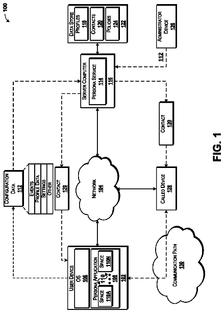
Multiple persona support for communications
Concepts and technologies are disclosed herein for providing multiple persona support for communications.
US 9,838,631 B2 · Assignee: CANON KABUSHIKI KAISHA · Inventors: Araoka; Yukio
Sheet 1 of 10 from the published document. All sheets in the USPTO PDF
A solid state imaging device includes a pixel circuit 102 configured to generate a pixel signal by photoelectric conversion, a reference signal generation circuit 115 configured to generate a reference signal which changes in level with time, and a plurality of comparators configured to, based on the reference signal generated by the reference signal generation circuit, compare a plurality of reference signals being given offset voltages differing from each other, with the pixel signal, or compare a plurality of pixel signals being given offset voltages differing from each other, with the reference signal.
Field of the Invention The present invention relates to a solid state imaging device and a method of driving the solid state imaging device. Description of the Related Art A solid state imaging device including an analog-digital converter is known (refer to, for example, Japanese Laid-Open Patent Publication No. 2008-098722 (Patent Reference 1)). As for a pixel array unit, unit pixels each including a photoelectric conversion element are two-dimensionally arranged in a matrix form, and a column signal line is wired every column in the matrix arrangement of the unit pixels. A row scanning unit selects and controls respective unit pixels in the pixel array unit every row. The analog-digital converter converts an analog signal output from a unit pixel in the row selected and controlled by the row scanning unit via the column signal line to a digital signal. The analog-digital converter incl
1 of 10 drawing sheets so far from the published document, cropped to the drawing. Every sheet is in the USPTO PDF.
What the patent claimed, word for word. All of it is now free to use.
Field of the Invention
The present invention relates to a solid state imaging device and a method of driving the solid state imaging device.
Description of the Related Art
A solid state imaging device including an analog-digital converter is known (refer to, for example, Japanese Laid-Open Patent Publication No. 2008-098722 (Patent Reference 1)). As for a pixel array unit, unit pixels each including a photoelectric conversion element are two-dimensionally arranged in a matrix form, and a column signal line is wired every column in the matrix arrangement of the unit pixels. A row scanning unit selects and controls respective unit pixels in the pixel array unit every row. The analog-digital converter converts an analog signal output from a unit pixel in the row selected and controlled by the row scanning unit via the column signal line to a digital signal. The analog-digital converter includes a first comparison unit, a second comparison unit, and a counting unit. The first comparison unit compares the analog signal with any one of a plurality of first reference voltages taking a slope shape and having inclinations which are identical with each other. The second comparison unit compares a second reference voltage which is different from the first reference voltage in slope inclination with any one of the plurality of the first reference voltages used in the first comparison unit. The counting unit conducts count operation with a count quantity depending upon comparison results in the first and second comparison units, and converts a count value to the digital signal.
A solid state imaging device includes a pixel circuit configured to generate a pixel signal by photoelectric conversion, a reference signal generation circuit configured to generate a reference signal which changes in level with time, and a plurality of comparators configured to, based on the reference signal generated by the reference signal generation circuit, compare a plurality of reference signals being given offset voltages differing from each other, with the pixel signal, or compare a plurality of pixel signals being given offset voltages differing from each other, with the reference signal.
Further features of the present invention will become apparent from the following description of exemplary embodiments with reference to the attached drawings.
FIG. 1 is a diagram illustrating a configuration example of a solid state imaging device according to a first embodiment of the present invention.
FIG. 2 is a circuit diagram illustrating a configuration example of a pixel circuit illustrated in FIG. 1 .
FIG. 3 is a circuit diagram illustrating a configuration example of a column amplifier circuit illustrated in FIG. 1 .
FIG. 4 is a timing chart illustrating a method of driving the solid state imaging device illustrated in FIG. 1 .
FIG. 5 is a diagram illustrating a configuration example of a solid state imaging device according to a second embodiment of the present invention.
FIGS. 6A, 6B and 6C are diagrams illustrating a method of controlling switches.
FIG. 7 is a timing chart illustrating a method of driving the solid state imaging device according to a third embodiment of the present invention.
FIG. 8 is a diagram illustrating a configuration example of a solid state imaging device according to a fourth embodiment of the present invention.
FIG. 9 is a diagram illustrating a configuration example of a solid state imaging device according to a fifth embodiment of the present invention.
FIG. 10 is a timing chart illustrating a method of driving the solid state imaging device illustrated in FIG. 9 .
FIGS. 11A, 11B and 11C are diagrams illustrating a method of controlling switches.
Preferred embodiments of the present invention will now be described in detail in accordance with the accompanying drawings.
In a solid state imaging device that converts an analog signal to a digital signal by comparing an analog signal with a reference voltage, it is difficult to reconcile a higher speed and a higher resolution of the conversion. In the solid state imaging device described in the Patent Reference 1, a higher resolution is attained, and consequently the speed is lowered.
A technique described hereafter relates to a solid state imaging device and a method of driving thereof capable of reconciling a higher speed and a higher resolution. A First Embodiment
FIG. 1 is a diagram illustrating a configuration example of a solid state imaging device according to a first embodiment of the present invention. A pixel array 101 includes a plurality of pixel circuits 102 arranged in a two-dimensional matrix form. Each of the plurality of pixel circuits 102 generates a pixel signal by photoelectric conversion.
FIG. 2 is a circuit diagram illustrating a configuration example of the pixel circuit 102 in FIG. 1 . The pixel circuit 102 includes a photoelectric conversion unit PD, a floating diffusion region FD, a transfer transistor 201 , a reset transistor 202 , an amplifier transistor 203 , and a select transistor 204 . The pixel circuit 102 generates the pixel signal by photoelectric conversion. The photoelectric conversion unit PD is, for example, a photodiode, and converts light to charge (electrons) and stores the charge (electrons). When a signal TX becomes a high level, the transfer transistor 201 turns on and transfers the charge stored in the photoelectric conversion unit PD to the floating diffusion region FD. The floating diffusion region FD stores charge and converts the charge to a voltage. The amplifier transistor 203 is connected at a drain thereof to a node of a power supply voltage VDD. The amplifier transistor 203 amplifies the voltage of the floating diffusion region FD and outputs a resultant voltage from a source thereof. When a signal SEL becomes a high level, the select transistor 204 turns on and outputs the voltage which is output from the source of the amplifier transistor 203 to a vertical output line 103 . When the signal RES becomes a high level, the reset transistor 202 turns on and resets the voltage of the floating diffusion region FD and/or the photoelectric conversion unit PD to the power supply voltage VDD. A row scanning circuit 114 in FIG. 1 outputs same signals TX, RES and SEL to the pixel circuits 102 on the same row under control of a timing generation circuit 117 .
In FIG. 1 , the vertical output lines 103 on respective columns are connected to the pixel circuits 102 in common on respective columns, respectively. Column processing circuits 104 on respective columns are connected to the vertical output lines 103 on respective columns, respectively. The column processing circuit 104 includes a column amplifier circuit 105 , switches 106 , capacitors 107 , a plurality of comparators 108 - 1 to 108 - n , a plurality of counters 109 - 1 to 109 - n , and a memory circuit 110 . The memory circuit 110 includes an S-memory 111 and an N-memory 112 .
FIG. 3 is a circuit diagram illustrating a configuration example of the column amplifier circuit 105 in FIG. 1 . The column amplifier circuit 105 includes a current source 302 , a switch SW 1 , an input capacitor Ci, a feedback capacitor Cf, a switch SW 2 , and a differential amplifier 301 . The current source 302 is connected between the vertical output line 103 and a ground potential node to constitute a source follower in conjunction with the amplifier transistor 203 in FIG. 2 . A series connection circuit of the switch SW 1 and the input capacitor Ci is connected between the vertical output line 103 and an inverted input terminal of the differential amplifier 301 . A reference voltage is input to a non-inverted input terminal of the differential amplifier 301 . A parallel connection circuit of the feedback capacitor Cf and the switch SW 2 is connected between the inverted input terminal and an output terminal of the differential amplifier 301 . The differential amplifier 301 conducts inverted amplification, and outputs a signal PIX. On/off operations of the switches SW 1 and SW 2 are controlled by the timing generation circuit 117 .
In FIG. 1 , a reference signal generation circuit 115 includes a buffer 116 . The reference signal generation circuit 115 generates one reference signal (ramp signal) Vref_ 1 which changes in level with time and a plurality of offset voltages (constant voltages) Vref_ 2 to Vref_n. The reference signal generation circuit 115 starts generation of the reference signal Vref_ 1 on the basis of a signal sig 3 which is input from the timing generation circuit 117 . The buffer 116 buffers the reference signal Vref_ 1 and outputs a reference signal R 1 . Furthermore, n−1 switches 106 are connected between nodes of n−1 offset voltages Vref_ 2 to Vref_n and inverted input terminals of the n−1 comparators 108 - 2 to 108 - n , respectively. The n−1 switches 106 are controlled in on/off by a signal sig 1 which is input from the timing generation circuit 117 . Furthermore, n−1 capacitors 107 are connected between the inverted input terminals of the n comparators 108 - 1 to 108 - n , respectively. Furthermore, n reference signals R 1 to Rn are input to the inverted input terminals of the n comparators 108 - 1 to 108 - n , respectively. The signal PIX is input to non-inverted input terminals of the n comparators 108 - 1 to 108 - n . The comparators 108 - 1 to 108 - n output a high level signal in a case where the signal PIX is greater than the reference signals R 1 to Rn, respectively. The comparators 108 - 1 to 108 - n output a low level signal in a case where the signal PIX is less than the reference signals R 1 to Rn, respectively.
The n counters 109 - 1 to 109 - n start counting synchronized to a clock signal CLK which is input from the timing generation circuit 117 in response to a signal sig 2 which is input from the timing generation circuit 117 . If output signals of the n comparators 108 - 1 to 108 - n change from a high level to a low level, the n counters 109 - 1 to 109 - n stop counting, respectively. At this time, only one of output signals of the n comparators 108 - 1 to 108 - n changes from the high level to the low level. A count value of one counter that is included in the n counters 109 - 1 to 109 - n and that stops in counting is written into the S-memory 111 or the N-memory 112 in accordance with a signal sig 4 which is input from the timing generation circuit 117 . The column scanning circuit 118 outputs values stored in the S-memory 111 or the N-memory 112 in the column processing circuit 104 on each column to a horizontal output line 113 in order.
FIG. 4 is a timing chart illustrating a method of driving the solid state imaging device illustrated in FIG. 1 . At time t 1 , the signal RES is at a high level, and consequently the reset transistor 202 is on and the floating diffusion region FD is reset to the power supply voltage VDD. Furthermore, since the signal SEL is at the high level, the select transistor 204 is on and a noise signal which is a signal at time when the pixel circuit 102 is in a reset state is output to the vertical output line 103 . Furthermore, the switches SW 1 and SW 2 turn on, and the inverted input terminal and the output terminal of the differential amplifier 301 are short-circuited to each other. As a result, the column amplifier circuit 105 is brought into a reset mode, and the column amplifier circuit 105 outputs the signal PIX functioning as a reset signal.
Furthermore, the switches 106 are turned on by the signal sig 1 of a low level. The reference signal generation circuit 115 starts generation of the voltages Vref_ 1 to Vref_n. The voltages Vref_ 1 to Vref_n are the offset voltages. As a result, the reference signals R 1 to Rn become an offset voltage of a plurality of levels.
Then, at time t 2 , the signals sig 2 and sig 3 become a high level. As a result, the reference signal generation circuit 115 starts generation of the reference signal (ramp signal) Vref_ 1 which changes in level with time. Accordingly, the reference signal R 1 also starts a level change with time in the same way as the reference signal Vref_ 1 . Furthermore, the comparison operation in the comparators 108 - 1 to 108 - n and the count operation in the counters 109 - 1 to 109 - n are started. The first comparator 108 - 1 outputs a high level for a period of t 2 to t 3 with the reference signal R 1 less than the reset signal PIX, and outputs a low level for a period of t 3 to t 4 with the reference signal R 1 greater than the reset signal PIX. By the way, since the reference signals R 2 to Rn are greater than the reset signal PIX, the comparators 108 - 2 to 108 - n maintain low-level outputs.
At time t 3 , the output of the first comparator 108 - 1 changes from the high level to the low level. As a result, the first counter 109 - 1 stops the count operation.
Then, at time t 4 , the reference signal generation circuit 115 finishes the generation of the reference signal Vref_ 1 which changes in level with time, and generates a signal of an offset voltage Vref_ 1 . The reference signal R 1 also becomes a constant voltage in the same way as the signal Vref_ 1 . Furthermore, the switch SW 1 turns off. Furthermore, the signal RES becomes the low level, and the reset switch 202 turns off.
Then, at time t 5 , the signal sig 4 becomes the high level, and a count value of the first counter 109 - 1 which stops in count operation is written into the N-memory 112 . This count value corresponds to a value obtained by conducting analog-digital conversion on the reset signal PIX. Furthermore, the switch SW 2 turns off, and the column amplifier circuit 105 is brought into a gain mode. Thereafter, the signal TX becomes the high level, and the transfer transistor 201 turns on. As a result, charge subjected to the photoelectric conversion in the photoelectric conversion unit PD is transferred to the floating diffusion region FD, and the pixel signal is output to the vertical output line 103 .
Then, at time t 6 , the signal sig 1 becomes the high level, and the switches 106 turn off. Furthermore, the signal sig 4 becomes the low level, and writing into the N-memory 112 is finished. Furthermore, the signal TX becomes the low level, and the transfer switch 201 turns off.
Then, at time t 7 , the switch SW 1 turns on and the column amplifier circuit 105 inverts and amplifies the pixel signal on the vertical output line 103 and outputs the signal PIX functioning as the pixel signal. A gain in this amplification is Ci/Cf.
Then, at time t 8 , the signals sig 2 and sig 3 become the high level. As a result, the reference signal generation circuit 115 starts generation of the reference signal (ramp signal) Vref_ 1 which changes in level with time. As a result, the reference signals R 1 to Rn start the level change with time because of coupling via the capacitors 107 , and become reference signals which differ in range of level change, respectively. By the way, the reference signals R 1 to Rn are not restricted to ramp signals, but may be reference signals which change in level stepwise with time. Furthermore, the comparison operation in the comparators 108 - 1 to 108 - n and the count operation in the counters 109 - 1 to 109 - n are started. The third comparator 108 - 3 outputs the high level for a period of t 8 to t 9 with the reference signal R 3 less than the pixel signal PIX, and outputs the low level for a period of t 9 and on with the reference signal R 3 greater than the pixel signal PIX. By the way, since the reference signals R 4 to Rn are greater than the pixel signal PIX, the comparators 108 - 4 to 108 - n maintain the low level outputs. Since the reference signals R 1 and R 2 are less than the pixel signal PIX, the comparators 108 - 1 and 108 - 2 maintain the high level outputs.
At time t 9 , the output of the third comparator 108 - 3 changes from the high level to the low level. As a result, the third counter 109 - 3 stops the count operation.
Thereafter, the reference signal generation circuit 115 stops generation of the reference signal Vref_ 1 which changes in level with time, and outputs signals Vref_ 1 to Vref_n of offset voltage of, for example, 0 V. As a result, the reference signals R 1 to Rn become a constant voltage of, for example, 0 V.
Then, at time t 10 , the signal sig 1 becomes the low level and the switches 106 turn on. Furthermore, the signal sig 4 becomes the high level, and a count value in the third counter 109 - 3 which has stopped the count operation is written into the S-memory 111 . This count value corresponds to a value obtained by applying analog-digital conversion to the pixel signal PIX. Furthermore, the signal RES becomes the high level, the reset switch 202 turns on, and the signal PIX becomes a reset signal. Furthermore, the switch SW 1 turns off. Thereafter, the count value in the N-memory 112 and the count value in the S-memory 111 are read out onto the horizontal output line 113 in order column to column by the column scanning circuit 118 , difference processing is conducted, and a noise component of the pixel signal is removed.
An offset voltage sampling period T 1 of the reference signals R 1 to Rn is a period of time t 1 to t 6 . A hold period T 3 of the reference signals R 1 to Rn is a period of time t 6 to t 10 . A reset signal read period T 2 is a period of time t 2 to t 4 . A pixel signal read period T 4 is a period of time t 8 to t 10 . The above-described processing with a row taken as the unit is conducted for all rows to obtain a two-dimensional image.
As described heretofore, the reference signal generation circuit 115 generates one reference signal R 1 which changes in level with time. The plurality of comparators 108 - 1 to 108 - n compares a plurality of reference signals R 1 to Rn being given the plurality of offset voltages Vref_ 2 to Vref_n based on one reference signal R 1 generated by the reference signal generation circuit 115 , with the pixel signal PIX. An offset unit includes a plurality of capacitors 107 connected between the inverted input terminals of the plurality of comparators 108 - 1 to 108 - n . The offset unit generates the plurality of reference signals R 1 to Rn by giving a plurality of offset voltages Vref_ 2 to Vref_n to one reference signal R 1 generated by the reference signal generation circuit 115 , and outputs the reference signals R 1 to Rn to the plurality of comparators 108 - 1 to 108 - n . The plurality of capacitors 107 store the plurality of offset voltages Vref_ 2 to Vref_n. The plurality of comparators 108 - 1 to 108 - n compare the plurality of reference signals R 1 to Rn with the pixel signal PIX.
In the present embodiment, the plurality of comparators 108 - 1 to 108 - n compare the reference signals R 1 to Rn of a plurality of level ranges with the pixel signal PIX, respectively at the same time. As a result, it is possible to reconcile a higher speed and a higher resolution of analog-digital conversion processing. A Second Embodiment
FIG. 5 is a diagram illustrating a configuration example of a solid state imaging device according to a second embodiment of the present invention. The present embodiment ( FIG. 5 ) is obtained by removing the switches 106 and capacitors 107 from the first embodiment ( FIG. 1 ) and adding the switches SW 3 and SW 4 , an inverter 501 , and capacitors 502 . Hereafter, points where the present embodiment differs from the first embodiment will be described. As illustrated in FIG. 6C , the inverter 501 logically inverts the signal sig 1 and generates a control signal of the switches SW 4 . The buffer 116 outputs a signal R 1 obtained by buffering the signal Vref_ 1 . The first comparator 108 - 1 is connected at a non-inverted input terminal thereof to a line of the signal PIX, and connected at an inverted input terminal to a line of the reference signal R 1 .
FIGS. 6A, 6B and 6C are diagrams illustrating a circuit operation example of comparators in the second embodiment of the present invention. The non-inverted input terminals of the comparators 108 - 2 to 108 - n are connected to the signal PIX or Vref_ 2 to Vref_n by the switches SW 3 , respectively. The inverted input terminals of the comparators 108 - 2 to 108 - n are connected to comparator outputs via the switches SW 4 and connected to the signal R 1 via the capacitors 502 . For a period T 11 with the signal sig 1 being at a low level in FIG. 6C , the switches SW 3 connect the non-inverted input terminals of the comparators 108 - 2 to 108 - n to lines of the signals Vref_ 2 to Vref_n, respectively as illustrated in FIG. 6A . The signals Vref_ 2 to Vref_n are offset voltages which are different from each other. For the period T 11 with the output signal of the inverter 501 being at the high level, the switches SW 4 turn on and short-circuit the inverted input terminals and the output terminals of the comparators 108 - 2 to 108 - n . As a result, offset voltages of the signals Vref_ 2 to Vref_n and offset voltages of the comparators 108 - 2 to 108 - n with respect to the reference signal R 1 are stored in the capacitors 502 . The period T 11 is a sampling period of the offset voltage.
Furthermore, for a period T 12 with the signal sig 1 being at the high level in FIG. 6C , the switches SW 3 connect the non-inverted input terminals of the comparators 108 - 2 to 108 - n to the line of the signal PIX, respectively, as illustrated in FIG. 6B . For the period T 12 with the output signal of the inverter 501 being at the low level, the switches SW 4 turn off. The period T 12 corresponds to the period T 3 in FIG. 4 , and the reference signal R 1 changes in level with time. Reference signals R 2 to Rn are signals of the inverted input terminals of the comparators 108 - 2 to 108 - n , respectively. Since the offset voltages between the reference signal R 1 and the signals Vref_ 2 to Vref_n are stored in capacitors 502 , the reference signals R 2 to Rn become signals obtained by adding the offset voltages of the signals Vref_ 2 to Vref_n to the reference signal R 1 , respectively. The first comparator 108 - 1 compares the signal PIX with the reference signal R 1 . The comparators 108 - 2 to 108 - n compare the signal PIX with the reference signals R 2 to Rn, respectively.
As described heretofore, the offset unit includes a plurality of capacitors 502 connected between the reference signal R 1 and the inverted input terminals of the plurality of comparators 108 - 2 to 108 - n . The offset unit generates a plurality of reference signals R 2 to Rn by giving a plurality of offset voltages Vref_ 2 to Vref_n to the reference signal R 1 , and outputs the reference signals R 2 to Rn to the plurality of comparators 108 - 2 to 108 - n . The plurality of capacitors 502 store the plurality of offset voltages Vref_ 2 to Vref_n in a state in which the output terminals and the inverted input terminals of the plurality of comparators 108 - 2 to 108 - n are short-circuited. Thereafter, the plurality of capacitors 502 input the reference signal R 1 in a state in which the output terminals of the plurality of comparators 108 - 2 to 108 - n are disconnected from the input terminals. The plurality of comparators 108 - 1 to 108 - n compare the plurality of reference signals R 1 to Rn generated by the reference signal generation circuit 115 with the pixel signal PIX.
In the present embodiment, the plurality of comparators 108 - 1 to 108 - n compare the plurality of reference signals R 1 to Rn being given the plurality of offset voltages Vref_ 2 to Vref_n based on one reference signal R 1 , with the pixel signal PIX, in the same way as the first embodiment.
In the present embodiment, the plurality of comparators 108 - 1 to 108 - n compare the reference signals R 1 to Rn with the pixel signal PIX, respectively at the same time. As a result, it becomes possible to reconcile a higher speed and a higher resolution of analog-digital conversion processing. A Third Embodiment
FIG. 7 is a timing chart illustrating a method of driving a solid state imaging device according to a third embodiment of the present invention. Hereafter, points where the present embodiment differs from the first embodiment will be described. For a period T 4 , the plurality of reference signals R 1 to Rn include areas 701 where respective level ranges overlap each other. Level ranges of the reference signals R 1 to Rn vary due to the manufacture variation in some cases. Even in that case, according to the present embodiment, it is possible to prevent any of outputs of the plurality of comparators 108 - 1 to 108 - n from being not inverted from the high level to the low level and it is possible to conduct analog-digital conversion certainly. A Fourth Embodiment
FIG. 8 is a diagram illustrating a configuration example of a solid state imaging device according to a fourth embodiment of the present invention. The present embodiment ( FIG. 8 ) is obtained by removing the first comparator 108 - 1 and the first counter 109 - 1 from the second embodiment ( FIG. 5 ). Reference signals R 2 to Rn obtained by adding offset voltages Vref_ 2 to Vref_n to the reference signal R 1 are input to all comparators 108 - 2 to 108 - n via capacitors 502 . The comparators 108 - 2 to 108 - n compare the reference signals R 2 to Rn with the pixel signal PIX. In this case, however, it is necessary to conduct the operation in the sampling period T 11 and the hold period T 12 in FIG. 6C , in a reset signal read period T 2 as well. In the present embodiment, it is possible to reconcile a higher speed and a higher resolution of analog-digital conversion processing in the same way as the second embodiment. A Fifth Embodiment
FIG. 9 is a diagram illustrating a configuration example of a solid state imaging device according to a fifth embodiment of the present invention. The present embodiment ( FIG. 9 ) is obtained by removing the first comparator 108 - 1 and the first counter 109 - 1 from the second embodiment ( FIG. 5 ). Pixel signals P 2 to Pn obtained by adding offset voltages Vref_ 2 to Vref_n to the pixel signal PIX are input to all comparators 108 - 2 to 108 - n via capacitors 502 . The comparators 108 - 2 to 108 - n compare the pixel signals P 2 to Pn with the reference signal R 1 . In this case, however, it is necessary to conduct the operation in the sampling period T 11 and the hold period T 12 in FIG. 6C , in a reset signal read period T 2 as well.
FIG. 10 is a timing chart illustrating a method of driving a solid state imaging device according to the present embodiment. In the operation illustrated in FIG. 4 , the reference signals R 1 to R 4 are compared with the pixel signal PIX for a period T 3 . In the present embodiment, the pixel signals P 1 to P 4 obtained by giving a plurality of offset voltages to the pixel signal PIX are compared with the reference signal R 1 during the period T 3 .
FIGS. 11A, 11B and 11C are diagrams illustrating how switch control is conducted. Operation is similar to that in FIGS. 6A to 6C , and consequently description thereof will be omitted.
In the present embodiment, it is possible to reconcile a higher speed and a higher resolution of analog-digital conversion processing as the second embodiment.
Since a plurality of comparators conduct the comparison, it is possible to reconcile a higher speed and a higher resolution.
While the present invention has been described with reference to exemplary embodiments, it is to be understood that the invention is not limited to the disclosed exemplary embodiments. The scope of the following claims is to be accorded the broadest interpretation so as to encompass all such modifications and equivalent structures and functions.
This application claims the benefit of Japanese Patent Application No. 2013-269556, filed Dec. 26, 2013, which is hereby incorporated by reference herein in its entirety.
About 5,115 words. The USPTO PDF has it with every drawing.
Fees are due 3.5, 7.5 and 11.5 years after grant. This patent expired on December 5, 2025, so the fee marked "not paid" was the one that went unpaid.
SOLID STATE IMAGING DEVICE AND METHOD OF DRIVING SOLID STATE IMAGING DEVICE
Filed Dec 2014 · published Jul 2015Solid state imaging device and method of driving solid state imaging device
Filed Dec 2014 · granted Dec 2017Earlier publications, parents and continuations. None of them can still be enforced, or this patent would not be listed.
Prior art cited by the examiner or applicant. Useful when you check your own idea for novelty.
Everything on this page comes from the documents linked above.