Cross reference to related application
This application claims the benefit of priority of Japanese Patent Application Number 2015-045008 filed on Mar. 6, 2015, the entire contents of which are hereby incorporated, by reference.
Background
1. Technical field
The present disclosure relates to lighting devices and lighting systems for performing visible light communication.
2. Description of the related art
Visible light communication systems for transmitting information by turning on and off a lighting device are known (refer to PCT International Publication No. WO 2014/103341, for example). In such visible light communication systems, for example, identification information for identifying the lighting device or position information indicating a position of the lighting device is superimposed onto light emitted by the lighting device and transmitted.
Summary
In some cases, however, the conventional visible light communication systems described above require a long time to obtain such information (light signal).
In view of this, an object of the present disclosure is to provide a lighting device and a lighting system which enable a receiver to obtain information ion in a short time period.
In order to achieve the above object, a lighting device according to an aspect of the present disclosure, which performs visible light communication with a receiver including an image sensor, includes: a dividing unit that divides identification information assigned to the lighting device into N packets (where N is a natural number greater than or equal to 2); a block generator that generates a plurality of signal blocks each of which includes M packets (where M is a natural number greater than or equal to N) that includes at least one of each of the N packets; and a light source that sequentially transmits the plurality of signal blocks in either one of (i) each frame cycle of the image sensor and (ii) each cycle substantially equal to an integral multiple of the frame cycle, by superimposing each of the plurality of signal blocks onto illumination light. The block generator generates the plurality of signal blocks so that an order of arranging the M packets is different between consecutive signal blocks in the plurality of signal blocks.
Furthermore, in order to achieve the above object, a lighting system according to another aspect of the present disclosure includes the lighting device and the receiver.
The present disclosure enables a receiver to obtain information in a short time period.
Brief description of drawings
The figures depict one or more implementations in accordance with the present teaching, by way of examples only, not by way of limitations. In the figures, like reference numerals refer to the same or similar elements.
FIG. 1 is a schematic diagram illustrating a lighting system according to a present embodiment.
FIG. 2 is a diagram illustrating an image captured by an image sensor included in a receiver according to the present embodiment.
FIG. 3 is a block diagram illustrating a structure of a lighting device according to the present embodiment.
FIG. 4 is a diagram illustrating identification information divided, into four pieces according to the present embodiment.
FIG. 5 is a diagram illustrating an example of a structure of signal blocks each of which includes identification information divided into four pieces (where M=5) according to the present embodiment.
FIG. 6A is a timing diagram indicating a transmission timing and a scan timing of each signal block according to the present embodiment.
FIG. 6B is a timing diagram indicating a transmission timing and a scan tinning of each signal block according to the present embodiment.
FIG. 7 is a timing diagram indicating another example of a transmission timing and a scan. timing of each signal block according to the present embodiment.
FIG. 8 is a diagram illustrating another example of a structure of signal blocks each of which includes identification information divided into four pieces (where M=7) according to the present embodiment.
FIG. 9 is a diagram illustrating still another example of a structure of signal blocks each of which includes identification information divided into four pieces (where M=11) according to the present embodiment.
FIG. 10 is a diagram illustrating an example of a structure of signal blocks each of which includes identification information divided into two pieces (where M=3) according to the present embodiment.
FIG. 11A is a diagram illustrating an example of a structure of signal blocks each of which includes identification information divided into three pieces (where M=4) according to the present embodiment.
FIG. 11B is a diagram illustrating another example of a structure of signal blocks each of which includes identification information divided into three pieces (where M=5) according to the present embodiment.
FIG. 11C is a diagram illustrating still another example of a structure of signal blocks each of which includes identification information divided into three pieces (where M=7) according to the present embodiment.
FIG. 12A is a diagram illustrating an example of a structure of signal blocks each of which includes identification information divided into four pieces (where M=5) according to the present embodiment.
FIG. 12B is a diagram illustrating another example of a structure of signal blocks each of which includes identification information divided into four pieces (where M=6) according to the present embodiment.
FIG. 12C is a diagram illustrating still another example of a structure of signal blocks each of which includes identification information divided into four pieces (where M=6) according to the present embodiment.
FIG. 12D is a diagram illustrating still another example of a structure of signal blocks each of which includes identification information divided into four pieces (where M=7) according to the present embodiment.
FIG. 13A is a diagram illustrating an example of a structure of signal blocks each of which includes identification information divided into five pieces (where M=6) according to the present embodiment.
FIG. 13B is a diagram illustrating another example of a structure of signal blocks each of which includes identification information divided into five pieces (where M=7) according to the present embodiment.
FIG. 13C is a diagram illustrating still another example of a structure of signal blocks each of which includes identification information divided into five pieces (where M=8) according to the present embodiment.
FIG. 13D is a diagram illustrating still another example of a structure of signal blocks each of which includes identification information divided into five pieces (where M=9) according to the present embodiment.
FIG. 14A is a diagram illustrating an example of a structure of signal blocks each of which includes identification information divided into six pieces (where M=7) according to the present embodiment.
FIG. 14B is a diagram illustrating another example of a structure of signal blocks each of which includes identification information divided into six pieces (where M=8) according to the present embodiment.
FIG. 14C is a diagram illustrating still another example of a structure of signal blocks each of which includes identification information divided into six pieces (where M=9) according to the present embodiment.
FIG. 14D is a diagram illustrating still another example of a structure of signal blocks each of which includes identification n information divided into six pieces (where M=10) according to the present embodiment.
FIG. 14E is a diagram illustrating still another example of a structure of signal blocks each of which includes identification information divided into six pieces (where M=11) according to the present embodiment.
FIG. 15A is a diagram illustrating an example of a structure of signal. blocks each of which includes identification information divided into seven pieces (where M=8) according to the present embodiment.
FIG. 15B is a diagram illustrating another example of a structure of signal blocks each of which includes identification information divided into seven pieces (where M=9) according to the present embodiment.
FIG. 15C is a diagram illustrating still another example of a structure of signal blocks each of which includes identification information divided into seven pieces (where M=10) according to the present embodiment.
FIG. 15D is a diagram illustrating still another example of a structure of signal blocks each of which includes identification information divided into seven pieces (where M=11) according to the present embodiment.
FIG. 15E is a diagram illustrating still another example of a structure of signal blocks each of which includes identification information divided into seven pieces (where M=12) according to the present embodiment.
FIG. 15F is a diagram illustrating still another example of a structure of signal blocks each of which includes identification information divided into seven pieces (where M=13) according to the present embodiment.
FIG. 16 is a block diagram illustrating a structure of a lighting device according to Variation 1 of the present embodiment.
FIG. 17 is a block diagram illustrating a structure of a receiver according to Variation 2 of the present embodiment.
Detailed description of embodiment
Hereinafter, a lighting device and a lighting system according to an exemplary embodiment are described in detail with reference to the accompanying drawings. The embodiment described below is a particular example. The numerical values, shapes, materials, elements, the arrangement and connection of the elements, steps, the order of the steps, and others indicated in the exemplary embodiment are merely examples, and therefore are not intended to limit the inventive concept. Thus, among the elements in the following embodiment, elements not recited in any of the independent claims defining the most generic part of the inventive concept are described as arbitrary elements.
The drawings are schematic diagrams, and do not necessarily provide strictly accurate illustration. In the respective diagrams, identical reference numerals are used throughout to designate identical elements. Embodiment
[Lighting System]
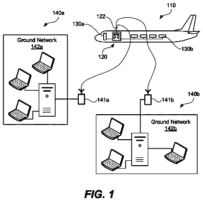
First, the outline of a lighting system (visible light communication system) according to a present embodiment will be described with reference to FIG. 1 . FIG. 1 is a schematic diagram illustrating lighting system 1 according to the present embodiment.
Lighting system 1 according to the present embodiment performs visible light communication in accordance with, for example, a communication system prescribed in CP-1223 “Visible Light Beacon System” (non-patent literature), Japan Electronics and Information Technology Industries Association (JEITA), May 2013.
As illustrated in FIG. 1 , lighting system 1 includes lighting device 10 and receiver 20 .
Lighting device 10 performs visible light communication with receiver 20 . For example, lighting device 10 illuminates the area around lighting device 10 by emitting illumination light (visible light). The illumination light is superimposed with identification information assigned. to lighting device 10 . In other words, the illumination light is a light signal including the identification information as a visible light communication signal. The structure of lighting device 10 will be described in more detail later with reference to FIG. 3 .
Receiver 20 performs visible light communication with lighting device 10 . Examples of receiver 20 include various portable information terminals, such as a portable telephone, a smartphone, and a tablet personal computer (tablet PC). Receiver 20 includes image sensor 21 as illustrated in FIG. 1 .
Image sensor 21 is an imaging device that receives illumination light (visible light) emitted by lighting device 10 . In the present embodiment, image sensor 21 uses a rolling shutter method.
FIG. 2 is a diagram illustrating image 30 captured by image sensor 21 included in receiver 20 according to the present embodiment. More specifically, FIG. 2 illustrates an image generated by image sensor 21 capturing lighting device 10 illustrated in FIG. 1 . Image 30 has illumination-light region 31 that shows illumination light received from lighting device 10 .
Illumination-light region 31 is, more specifically, a region showing an image of lighting device 10 . Receiver 20 can obtain the identification information transmitted by lighting device 10 , by detecting a light intensity (an amount of the received illumination light) on illumination-light region 31 .
A direction of scanning performed by image sensor 21 using a rolling shutter method is, for example, the positive direction of an x-axis as illustrated in FIG. 2 . Image sensor 21 can capture one frame of image 30 per scan.
Image sensor 21 repeats the scanning in each predetermined frame cycle to sequentially capture images 30 . A frame rate of image sensor 21 is, for example, 30 frames per second. In other ords, a frame cycle (hereinafter, referred to also as a “frame period”) is approximately 33.3 msec. It should be noted that the frame rate of image sensor 21 is not particularly limited. The frame rate may be, for example, 60 frames per second.
[Lighting Device]
FIG. 3 is a block diagram illustrating the structure of lighting device 10 according to the present embodiment. As illustrated in FIG. 3 , lighting device 10 includes memory 12 in which identification infbrmation 11 is stored, dividing unit 13 , block generator 14 , and light source 15 .
An example of identification information 11 is information for unique identifying lighting device 10 . Examples of identification information 11 include identification information uniquely assigned to lighting device 10 and position information indicating a position of lighting device 10 . Identification information 11 has a predetermined bit length. For example, a bit length of identification information 11 is 128 bits.
Memory 12 is a storage device in which identification information 11 is stored. An example of memory 12 is a semiconductor memory, such as a Read Only Memory (ROM).
Dividing unit 13 divides identification information 11 into N packets, where N is a natural number greater than or equal to 2. More specifically, dividing unit 13 reads identification information 11 from memory 12 and divides identification information 11 by a predetermined division number N to generate N packets.
It should be noted that receiver 20 cannot restore identification information 11 until all the divided N packets have been received. Missing of even one of the N packets prevents receiver 20 from restoring identification information 11 .
Each of the N packets is uniquely assigned with a packet number in a range from 1 to N. inclusive, for example. The following describes an example where N=4.
FIG. 4 is a diagram illustrating identification information 11 that is divided into four pieces according to the present embodiment.
As illustrated in FIG. 4 , identification information 11 is divided into four packets. The four packets have the same size (bit number), for example. For example, if identification information 11 has 128 bits, each of the four packets has 32 bits.
The four packets are respectively assigned with packets numbers from “1” to “4”. Hereinafter, for explanatory convenience, a packet number is expressed as P added with a numeral, such as “P 1 ”. An expression “packet P” with a numeral, such as “Packet P 1 ”, means a packet having a packet number represented by the numeral (for example, 1).
Referring back to FIG. 3 , block generator 14 generates a plurality of signal blocks. Each of the signal blocks consists of M packets, where M is a natural number greater than or equal to N. The M packets in each of the signal blocks include at least one of each of the N packets. In other words, each of the signal blocks includes at least one identification information 11 .
Block generator 14 generates the plurality of signal blocks so that an order of arranging packets is different among consecutive signal blocks in the plurality of signal blocks, More specifically, block generator 14 generates the plurality of signal blocks so that the Lth packet in a signal block is different from the Lth packet in another signal block to be transmitted immediately before the signal block. Here, L is a natural number in a range from 1 to M, inclusive,
In the present embodiment, block generator 14 generates the plurality of signal blocks so that the Lth packet is different between consecutive N signal blocks in the plurality of signal blocks. For example, L is an arbitrary natural number in a range from 1 to M, inclusive, In other words, block generator 14 generates the plurality of signal blocks so that the Lth packet placed at an arbitrary Lth position is different between consecutive N signal blocks in the plurality of signal blocks.
The processing performed by block generator 14 and the structure of the signal blocks will be described in more detail later.
It should be noted that, in the present embodiment, each of the expressions “immediately before”, “immediately after”, and “adjacent” means that no other signal block is transmitted therebetween. For example, if it is described that a second signal block is transmitted “immediately before” a first signal block, no other signal block is transmitted between the transmission of the second signal block and the transmission of the first signal block. Similarly, no other signal block is transmitted between transmission of a signal block and transmission of another signal block “immediately before” the signal block, and between transmissions of “adjacent” signal blocks.
Light source 15 sequentially transmits the plurality of signal blocks in each frame cycle of image sensor 21 by superimposing each of the signal blocks onto illumination light. For example, light source 15 transmits the plurality of signal blocks generated by block generator 14 , sequentially in a predetermined. order and in synchronization with a start of scanning performed by image sensor 21 . In this way, light source 15 repeatedly transmits identification information 11 .
Light source 15 includes light emitting element 15 a, such as a plurality of Light Emitting Diodes (LEDs). Examples of the LEDs are white LEDs. Light source 15 may include a laser element, an organic Electro Luminescence (EL) device, or an inorganic EL device, instead of LEDs. Light source 15 further includes, for example, drive circuit 15 b that drives light emitting element 15 a. Drive circuit 15 b drives light emitting element 15 a based on an output of block generator 14 . Drive circuit 15 b includes, for example, circuit parts such as a plurality of transistors.
Light source 15 switches a light intensity of the LEDs (for example, switches on and off the LEDs) to superimpose signal blocks onto illumination light, thereby transmitting the signal blocks. For example, light source 15 includes a transistor and a signal generator. The transistor switches on and off the LEDs. The signal generator generates a gate signal for controlling the switching of the transistor. The signal generator generates the gate signal according to the plurality of signal blocks generated by block generator 14 and the frame cycle of image sensor 21 .
The frame cycle of image sensor 21 is indicated by receiving-cycle information that is held in, for example, memory 12 . Alternatively, lighting device 10 may obtain the receiving-cycle information from the outside. An example of how to obtain the receiving-cycle information will be described later according to a variation of the present embodiment.
It should be noted that, as illustrated in FIG. 3 , dividing unit 13 and block generator 14 are realized by, for example,control circuit 17 , such a Central Processing Unit (CPU) or a microcomputer. Control circuit 17 includes a processor, input/output ports, a volatile memory, and the like. Control circuit 17 performs the functions of dividing unit 13 and block generator 14 by, for example, reading program 18 from memory 19 holding program 18 and executing program 18 . Memory 19 is a non-volatile memory, such as a flash memory.
[Signal Block]
FIG. 5 is a diagram illustrating an example of the structure of signal blocks each of which includes identification information 11 divided into four packets according to the present embodiment. FIG. 5 illustrates an example where the number M of packets included in each of four signal blocks Bi to B 4 is five.
Signal block B 1 is a signal block to be transmitted at time f 0 . Signal block B 1 includes packet P 1 , packet P 2 , packet P 3 , packet P 4 , and packet P 1 in this order.
Signal block B 2 is a signal block to be transmitted at time f 1 , immediately after signal block B 1 . Signal block B 2 includes packet P 2 , packet P 3 , packet P 4 , packet P 1 , and packet P 2 in this order.
Signal block B 3 is a signal block to be transmitted at time f 2 , immediately after signal block B 2 . Signal block B 3 includes packet P 3 , packet P 4 , packet P 1 , packet P 2 , and packet P 3 in this order.
Signal block B 4 is a signal block to he transmitted at time f 3 , immediately after signal block B 3 . Signal block B 4 includes packet P 4 , packet P 1 , packet P 2 , packet P 3 , and packet P 4 in this order.
As illustrated in FIG. 5 , each of signal blocks B 1 to B 4 includes packet P 1 as a packet next to packet P 4 . In other words, each of signal blocks B 1 to B 4 includes five packets so that a sequence of packets “P 1 ” to “P 4 ” is repeated throughout signal blocks B 1 to B 4 .
In the present embodiment, block generator 14 generates a plurality of signal blocks so that the N packets are repeatedly transmitted in a predetermined order of packet numbers. An example of the predetermined order is an ascending order of the packet numbers.
More specifically, packet numbers are sequential in a predetermined order throughout consecutive signal blocks. For example, if N packets arranged in an ascending order of packet numbers is repeatedly transmitted, the packets numbers are sequential in the ascending order throughout consecutive signal blocks. In other words, a packet number of the first packet in a signal block among a plurality of signal blocks is next in the ascending order to a packet number of the last packet in another signal block to be transmitted immediately before the signal block.
For example, as illustrated in FIG. 5 , since a packet number of the last packet in signal block B 1 is “P 1 ”, a packet number of the first packet in signal block B 2 is “P 2 ”. Likewise, packet numbers are sequential also between signal block B 2 and signal block B 3 and between signal block B 3 and signal block B 4 . Lighting device 10 sequentially transmits four signal blocks B 1 to B 4 in this order. In other words, a sequence of the four packets arranged in an ascending order of packet numbers (packets P 1 to P 4 ) is repeatedly transmitted.
Furthermore, according to the present embodiment, a shift amount is, for example, (i) a value other than a divisor of N or a value of 1. The shift amount is a value representing an amount of shift between packet numbers of adjacent signal blocks.
More specifically, the shift amount indicates a difference between a packet number of the Lth packet in a signal block among the plurality of signal blocks (hereinafter, referred to as a “first packet number”) and a packet number of the Lth packet in another signal block transmitted immediately before the signal block (hereinafter, referred to as a “second packet number”). The shift amount is, for example, a value obtained by subtracting the second packet number from the first packet number. However, if the first packet number is smaller than the second packet number, the shift amount is determined to be a value obtained by subtracting the second packet number from a value obtained by adding N to the first packet number.
In the example illustrated in FIG. 5 , the shift amount at an arbitrary position L is the same between any adjacent signal blocks. Specifically, in this example, the shift amount is 1. In other words, in FIG. 5 , whichever position is selected to compare packets, the difference in packet number (shift amount) is the same between any adjacent signal blocks.
In the present embodiment, for example, lighting device 10 repeats transmission of four signal blocks B 1 to B 4 . More specifically, signal block B 1 is transmitted after signal block B 4 . For example, the division number N is equal to the number of signal blocks included in a sequence of signal blocks which is repeatedly transmitted. For example, if identification information 11 is divided into N packets, block generator 14 generates N unique signal blocks. Light source 15 repeatedly transmits a sequence of the N unique signal blocks.
[Transmission Timing and Scan Timing (Matching Case)]
FIG. 6A and FIG. 6B are timing diagrams indicating the timing at which transmission of a signal block starts (referred to also as a “transmission timing”) and the timing at which scan starts (referred to also as a “scan timing”) according to the present embodiment. FIG. 6A and FIG. 6B show examples where the scan timing and the transmission timing match each other.
For example, image sensor 21 starts scanning at time f 0 , time f 1 , and time f 2 . In the present embodiment, a frame rate of image sensor 21 is approximately 30 fps. Therefore, in the case where time f 0 is 0 second, time f 1 is 1/30 second (approximately 33.3 msec) and time f 2 is 2/30 seconds (approximately 66.6 msec).
As illustrated in FIG. GA and FIG. 6B , light source 15 sequentially transmits signal block B 1 , signal block B 2 , and signal block B 3 at time f 0 , time f 1 , and time f 2 , respectively.
In these examples, if image sensor 21 captures an image of lighting device 10 on a sufficiently large region, for example if illumination-light region 31 illustrated in FIG. 2 is substantially equal to image 30 in size, receiver 20 can receive all the five packets included in signal block B 1 in one frame period. In other words, receiver 20 can restore identification information 11 because receiver 20 can receive packets P 1 to P 4 in one frame period.
On the other hand, if image sensor 21 captures an image of lighting device 10 on a small region, for example if illumination-light region 31 can show oniy a part of image 30 as illustrated in FIG. 2 , receiver 20 cannot receive all packets P 1 to P 4 in one frame period. More specifically, receiver 20 can receive only packet(s) that is/are transmitted in a predetermined part (receivable period 40 hatched in FIG. 6B ) of one frame period.
Receivable period 40 corresponds to a size of illumination-light region 31 . More specifically, receivable period 40 is a period during which image sensor 21 using a rolling shutter method scans illumination-light region 31 . Image sensor 21 can receive only illumination light that is emitted by lighting device 10 during scanning of illumination-light region 31 , in other words, during receivable period 40 .
For example, in a period before receivable period 40 , image sensor 21 scans a region located in the negative direction of the x-axis with respect to illumination-light region 31 , in other words, a region on which illumination light cannot be received. Therefore, image sensor 21 cannot receive illumination light in this period. For the same reason, image sensor 21 fails to receive illumination light also in a period after receivable period 40 .
In general, illumination-light region 31 appears at substantially the same position on different frames unless receiver 20 moves at a high speed. Therefore, the position of receivable period 40 in one frame period is substantially the same among a plurality of frames. In other words, there is a high possibility that receiver 20 can receive packets placed at the same position in an order among the frames.
For example, as illustrated in FIG. 6B , in a period from time f 0 to time f 1 , receiver 20 receives only the second packet of signal block B 1 , namely, packet P 2 . Subsequently, in the same manner, in a period from time f 1 to time f 2 , receiver 20 receives only the second packet of signal block B 2 , namely, packet P 3 . In a period from time f 2 to time f 3 , receiver 20 receives only the second packet of signal block B 3 , namely, packet P 4 .
In the present embodiment, as illustrated in FIG. 5 , a plurality of signal blocks are generated so that the Lth packet in a signal block is different from the Lth packet in another signal block to be transmitted immediately before the signal block. More specifically, with regard to the Lth packet in each of generated signal blocks, a packet number is successively incremented by 1 in the signal blocks.
Therefore, for example, if only the second packet (marked by a circle in FIG. 5 ) can be received from each signal block, receiver 20 can receive packet P 2 from signal block B 1 in the first frame. Subsequently, in the same manner, receiver 20 receives packet P 3 from signal block B 2 in the second frame, receives packet P 4 from signal block B 3 in the third frame, and receives packet P 1 from signal block B 4 in the fourth frame. As a result, receiver 20 can receive packets P 1 to P 4 in the four frame periods to restore identification information 11 .
If a packet number of the lath packet is not different among signal blocks, for example, if an order of packet numbers is the same among all the signal blocks, receiver 20 receives the same packets only. For example, receiver 20 receives only packets P 2 in frame periods. Receiver 20 thus cannot restore identification information 11 until receiver 20 receives the other packets accidentally (for example, due to move of receiver 20 ). As a result, the obtainment of identification information 11 requires a long time.
In contrast, in the present embodiment, a packet number of the Lth packet is different among signal blocks. It is therefore possible to respectively receive different packets in different frame periods as described previously. As a result, receiver 20 can obtain identification information 11 in a short time period.
If a plurality of packets can be received in one frame period, receiver 20 can restore identification information 11 in a shorter time period.
For example, if the second and third packets can be received in one frame period, receiver 20 can receive packet P 2 and packet P 3 from signal block B 1 in the first frame. In the second frame, receiver 20 receives packet. P 3 and packet P 4 from signal block 132 . Here, as packet P 3 has already been received, newly received packet P 3 is discarded. In the third frame, receiver 20 receives packet P 4 and packet P 1 from signal block B 3 . As a result, receiver 20 receives packets P 1 to P 4 in the three frame periods to restore identification information 11 .
Similarly, for example, if three packets can be received in one frame period, receiver 20 receives packets P 1 to P 4 in two frame periods to restore identification information 11 . If four packets can be received in one frame period, receiver 20 receives packets P 1 to P 4 in one frame period as illustrated in FIG. GA, and thereby restores identification information 11 .
Thus, according to the present embodiment, receiver 20 can restore identification information 11 by receiving packets P 1 to P 4 in maximum four frame periods.
[Transmission Timing and Scan Timing (Not-Matching Case)]
FIG. 7 is a timing diagram indicating another example of the timing at which transmission of a signal block starts (transmission timing) and the timing at which scan starts (scan timing) according to the present embodiment.
Although FIG. 6A and FIG. 6B illustrate the examples where the scan timing and the transmission timing match each other for each signal block, the present disclosure is not limited to these examples. As illustrated in FIG. 7 , it is also expected that there is a time lag between the scan timing and the transmission timing.
If there is a time lag between the scan timing and the transmission timing, receiver 20 cannot receive a packet that is being transmitted at a start (or end) of scanning. For example, as illustrated in. FIG. 7 , receiver 20 cannot receive packet P 4 that is being transmitted at time f 1 . In the first frame, receiver 20 can receive only packets P 1 to P 3 .
In this example, if a packet number of the Lth packet is not different among the signal blocks, for example, if an order of packet numbers is the same among all the signal blocks, receiver 20 never receives the fourth packet, namely, packet P 4 . Receiver 20 thus cannot restore identification information 11 until receiver 20 receives packet P 4 accidentally (for example, due to move of receiver 20 ). As a result, the obtainment of identification information 11 requires a long time.
In contrast, in the present embodiment, with regard to the Lth packet in each of signal blocks, a packet number is successively incremented by 1 in the signal blocks. As a result, in the example illustrated in FIG. 7 , receiver 20 can receive packets P 2 to P 4 in the second frame. Receiver 20 can eventually receive packets P 1 to P 4 in two frame periods to restore identification information 11 .
[Other Examples of Signal Blocks]
Referring to FIG. 8 and FIG. 9 , other examples of signal blocks in the case where identification information 11 is divided into four packets are described below. FIG. 8 and FIG. 9 illustrate other examples of a structure of signal blocks each of which includes identification information 11 divided into four packets according to the present embodiment. More specifically, FIG. 8 illustrates an example where M=7 and a shift amount=3, and FIG. 9 illustrates an example where M=11 and a shift amount=3.
For example, if a length of a packet (packet length) is shorter, more packets can be transmitted in one frame period. In other words, as illustrated in FIG. 8 and FIG. 9 , a single signal block includes more packets. For example, in the example illustrated in FIG. 9 , a single signal block includes two pieces of same identification information 11 . In other words, a single signal block includes at least two packets of each of four packets P 1 to P 4 .
As a packet is shorter, more packets can be included in receivable period 40 . It is therefore possible to receive thur packets in a shorter time period to restore identification information 11 .
Furthermore, even if receivable period 40 is short, in other words, even if illumination-light region 31 is small, a shorter length of a packet increases a possibility of receiving packet(s). It is therefore possible to obtain identification information 11 from a smaller image of lighting device 10 , for example, from lighting device 10 at a greater distance.
[Other Examples]
Referring to FIGS. 10 to 15F , examples of division number N, by which. identification information 11 is divided into packets, and signal blocks generated according to division number N are described. In each of the figures, each of a region framed by a thick line, a region framed by a thick broken line, and each of regions illustrated by predetermined hatchings or dots includes identification information 11 . In other words, receiving of packets included in each of these regions enables receiver 20 to restore identification information 11 .
The following describes patterns for restoring identification information 11 . More specifically, the following describes various combinations of (i) the number of packets receivable in one frame period and (ii) the number of frame periods required for receiving the N packets, in which either the number of receivable packets or the number of required frame periods is minimum. For example, in the case where receiving of three packets in two frame periods can restore identification information 11 , the restoration of identification information 11 is also possible (i) if at least four packets can be received in two frame periods and (ii) if three packets are received in at least three frame periods.
It should be noted that the division number and the signal blocks are not limited to the following examples. Furthermore, the patterns for restoring identification information 11 are not limited to the following examples, either. Example 1 N=2
FIG. 10 is a diagram illustrating an example of a structure of signal blocks each of which includes identification information 11 divided into two packets (where M=3) according to the present embodiment. As illustrated in FIG. 10 , receiver 20 can restore identification information 11 , if two packets are received in one frame period and if one packet is received in each of two frame periods. Example 2 N=3
FIGS. 11A to 11C are diagrams illustrating examples of a structure of signal blocks each of which includes identification information 11 divided into three packets according to the present embodiment. More specifically, FIG. 11A illustrates an example where M=4, FIG. 11B illustrates an example where M=5, and FIG. 11C illustrates an example where M=7.
As illustrated in FIGS. 11A to 11C , receiver 20 can restore identification information 11 in the following cases: (i) where three packets are received in one frame period, (ii) where two packets are received in each of two frame periods, and (iii) where one packet is received in each of three frame periods. Example 3 N=4
FIGS. 12A to 12D are diagrams illustrating examples of a structure of signal blocks each of which includes identification information 11 divided into four packets according to the present embodiment. More specifically, FIG. 12A illustrates an example where M=5, FIG. 12B illustrates an example where M=6, FIG. 12C illustrates an example where M=6, and FIG. 12D illustrates an example where M=7.
As illustrated in FIGS. 12A to 12D , receiver 20 can restore identification information 11 in the following cases: (i) where four packets are received in one frame period, (ii) where three packets are received in each of two frame periods, (iii) where two packets are received in each. of three frame periods, and (iv) where one packet is received in each of four frame periods. It should be noted that FIG. 12A is the same as FIG. 5 described above, and that FIG. 12D is the same as FIG. 8 described above.
The example of FIG. 12B illustrates the case where a shift amount is two, in other words, a divisor of N. In this case, for example, packet numbers of the first packets in the signal blocks appear alternately “1” and “3”. Therefore, if one packet is received in each of four frame periods, there is a risk that all the four kinds of packets cannot be received.
Therefore in the example illustrated in FIG. 12B , receiver 20 can restore identification information 11 (i) if four packets are received in one frame period and (ii) if two packets are received in each of two frame periods.
In the case where a shift amount is a divisor of N, the structure of a plurality of signal blocks as illustrated in FIG. 12C can increase the patterns for restoring identification information 11 . In the example illustrated in FIG. 12C , receiver 20 can restore identification information 11 in the following cases: (i) where four packets are received in one frame period, (ii) where three packets are received in each of two frame periods, (iii) where two packets are received in each of three frame periods, and (iv) where one packet is received in each of four frame periods.
In the example illustrated in FIG. 12C , identification information 11 may be restored also if two packets are received in each of two frame periods. For example, if the first and second packets are received in each of two frame periods, receiver 20 can restore identification information 11 by receiving the first and second packets from each of signal block B 3 and signal block B 4 (or from each of signal block B 1 and signal block B 2 ). Example 4 N=5
The description continues in the full USPTO document.
 Lapsed, fee not paid9 drawings