 Lapsed, fee not paid16 drawings
Hardware & Electronics · US 9,847,771 B2
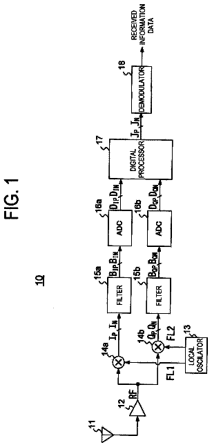
Filter circuit in wireless receiver
A filter circuit for generating a filtered signal includes a first filter unit, a second filter unit, and a negative feedback resistor.
US 9,847,813 B2 · Assignee: SONY CORPORATION · Inventors: Haseno; Shinichi et al.
Sheet 1 of 9 from the published document. All sheets in the USPTO PDF
A feed unit includes: a power transmission section configured to perform power transmission with use of a magnetic field or an electronic field; a power limiting section provided on a power supply line from an external power source to the power transmission section; and a control section provided on a side closer to the external power source than the power limiting section, and including a power transmission control section, the power transmission control section being configured to control the power transmission.
In recent years, a feed system (a non-contact feed system, or a wireless charging system) performing non-contact power supply (power transmission) on consumer electronics devices (CE devices) such as mobile phones and portable music players has attracted attention. Accordingly, charging is allowed to be started by not inserting (connecting) a connector of a power supply such as an AC adapter into a unit but placing an electronic apparatus (a secondary-side unit) on a charging tray (a primary-side unit). In other words, terminal connection between the electronic apparatus and the charging tray is unnecessary. As a method of performing non-contact power supply in such a way, an electromagnetic induction method is well known. In addition, a non-contact feed system using a method called magnetic resonance method which uses electromagnetic resonance phenomenon has attracted attention. Such a
1 of 9 drawing sheets so far from the published document, cropped to the drawing. Every sheet is in the USPTO PDF.
What the patent claimed, word for word. All of it is now free to use.
The present disclosure relates to a feed system performing non-contact power supply (power transmission) on a unit to be fed with power such as an electronic apparatus, and to a feed unit applied to such a feed system.
In recent years, a feed system (a non-contact feed system, or a wireless charging system) performing non-contact power supply (power transmission) on consumer electronics devices (CE devices) such as mobile phones and portable music players has attracted attention. Accordingly, charging is allowed to be started by not inserting (connecting) a connector of a power supply such as an AC adapter into a unit but placing an electronic apparatus (a secondary-side unit) on a charging tray (a primary-side unit). In other words, terminal connection between the electronic apparatus and the charging tray is unnecessary.
As a method of performing non-contact power supply in such a way, an electromagnetic induction method is well known. In addition, a non-contact feed system using a method called magnetic resonance method which uses electromagnetic resonance phenomenon has attracted attention. Such a non-contact feed system has been disclosed in, for example, PTLs 1 to 6. CITATION LIST Patent Literature
PTL 1: Japanese Unexamined Patent Application Publication No. PTL 2: International Publication No. WO00-27531 PTL 3: Japanese Unexamined Patent Application Publication No. 2008-206233 PTL 4: Japanese Unexamined Patent Application Publication No. 2002-34169 PTL 5: Japanese Unexamined Patent Application Publication No. 2005-110399 PTL 6: Japanese Unexamined Patent Application Publication No. 2010-63245 SUMMARY OF INVENTION
Incidentally, in the non-contact feed system described above, the load state of the feed unit is changed depending on situations, and for example, may be changed to overload state in some cases. Therefore, even in the case where such load change occurs, securement of proper control in the feed unit is demanded. Therefore, proportion of a method that is capable of achieving proper control irrespective of the load state in power transmission (non-contact power feeding) using a magnetic field or the like, is desired.
It is desirable to provide a feed unit and a feed system that are capable of achieving proper control irrespective of the load state in power transmission using a magnetic field or an electric field.
According to an embodiment of the present disclosure, there is provided a feed unit including: a power transmission section configured to perform power transmission with use of a magnetic field or an electric field; a power limiting section provided on a power supply line from an external power source to the power transmission section; and a control section provided on a side closer to the external power source than the power limiting section, and including a power transmission control section that is configured to control the power transmission.
According to an embodiment of the present disclosure, there is provided a feed system provided with one or a plurality of electronic apparatuses (units to be fed with power) and a feed unit that is configured to perform power transmission on the electronic apparatuses. The feed unit includes: a power transmission section configured to perform the power transmission with use of a magnetic field or an electronic field; a power limiting section provided on a power supply line from an external power source to the power transmission section; and a control section provided on a side closer to the external power source than the power limiting section, and including a power control section that is configured to control the power transmission.
In the feed unit and the feed system according to the respective embodiments of the present disclosure, the control section is provided on a side closer to the external power source than the power limiting section. Therefore, for example, even in the case of the overload state or the like, the power supply from the external power source to the control section side is not limited. Specifically, the power supply to the control section side is constantly ensured, and preferential power distribution to the control section side is performed.
In the feed unit and the feed system according to the respective embodiments of the present disclosure, the control section is provide on a side closer to the external power source than the power limiting section. Therefore, the power supply from the external power source to the control section side is constantly ensured, and preferential power distribution to the control section side is performed. Consequently, stable operation of the control section is ensured, and proper control is achieved irrespective of the load state in the power transmission using a magnetic field or an electronic field.
FIG. 1 is a perspective view illustrating an appearance configuration example of a feed system according to a first embodiment of the present disclosure.
FIG. 2 is a block diagram illustrating a detailed configuration example of the feed system illustrated in FIG. 1 .
FIG. 3 is a circuit diagram illustrating a detailed configuration example of each block illustrated in FIG. 2 .
FIG. 4 is a timing waveform chart illustrating an example of a control signal to an AC signal generation circuit.
FIG. 5 is a timing chart illustrating an example of a feeding period and a communication period.
FIG. 6 is a timing waveform chart illustrating an example of communication operation by pulse width modulation with use of the AC signal generation circuit.
FIG. 7 is a characteristic diagram schematically illustrating an example of drooping characteristics in an overload state.
FIG. 8 is a timing waveform chart for explaining power limiting distribution function in the overload state.
FIG. 9 is a schematic diagram for explaining forcible operation stop function and forcible power supply interruption function.
FIG. 10 is a circuit diagram illustrating a configuration example of a main part in a feed system according to a second embodiment.
FIG. 11 is a timing chart illustrating an operation example of a power limiting modulation circuit illustrated in FIG. 10 .
FIG. 12 is a timing waveform chart illustrating an example of communication operation by amplitude modulation with use of the power limiting modulation circuit illustrated in FIG. 10 .
FIG. 13 is a block diagram illustrating a schematic configuration example of a feed system according to a modification.
FIG. 14 is a schematic diagram illustrating an example of propagation state of an electric field in the feed system illustrated in FIG. 13 .
Some embodiments of the present disclosure will be described in detail below with reference to drawings. Note that description will be given in the following order.
1. First embodiment (an example of performing communication by pulse width modulation with use of an AC signal generation circuit)
2. Second embodiment (an example of also performing communication by amplitude modulation with use of a power limiting circuit)
3. Modifications (an example of a feed system performing non-contact power transmission using an electric field, etc.) First Embodiment
(General Configuration of Feed System 4 )
FIG. 1 illustrates an appearance configuration example of a feed system (a feed system 4 ) according to a first embodiment of the present disclosure, and FIG. 2 illustrates a block configuration example of the feed system 4 . The feed system 4 is a system (a non-contact feed system) performing non-contact power transmission (power supply, power feeding, or power transmission) with use of a magnetic field (with use of magnetic resonance, electromagnetic induction, and the like, hereinafter the same). The feed system 4 includes a feed unit 1 (a primary-side unit), and one or a plurality of electronic apparatuses (in this case, two electronic apparatuses 2 A and 2 B, secondary-side units) as units to be fed with power.
As illustrated in FIG. 1 , for example, in the feed system 4 , the electronic apparatuses 2 A and 2 B are placed (or closely disposed) on a feeding surface (a power transmission surface) S 1 of the feed unit 1 so that the power transmission is performed from the feed unit 1 to the electronic apparatuses 2 A and 2 B. In this case, in consideration of the case where the power transmission is performed to the plurality of electronic apparatuses 2 A and 2 B at the same time or in a time-divisional manner (sequentially), the feed unit 1 has a mat shape (a tray shape) in which an area of the feeding surface S 1 is larger than the size of the electronic apparatuses 2 A and 2 B, etc., to be fed with power.
(Feed Unit 1 )
As described above, the feed unit 1 is a unit (a charging tray) transmitting power (performing power transmission) to the electronic apparatuses 2 A and 2 B with use of a magnetic field. As illustrated in FIG. 2 , for example, the feed unit 1 may include a power transmission section 110 , a current detection circuit 111 , a power limiting circuit 112 , a power transmission device 11 including an AC signal generation circuit (high-frequency power generation circuit) 113 and an operation stop circuit 114 , and a data transmission section 13 . Moreover, the feed unit 1 may include a control section 10 including a power transmission control section (a modulation processing section) 10 A that is provided in the power transmission device 11 and a data transmission control section 10 B that is provided outside the power transmission device 11 . Among them, the power limiting circuit 112 , the AC signal generation circuit 113 , the operation stop circuit 114 , and the data transmission control section 10 B correspond to specific examples of “power limiting section”, “AC signal generation section”, “operation stop section”, and “data transmission control section”, respectively.
The power transmission section 110 is configured to include a power transmission coil (a primary-side coil) L 1 , capacitors C 1 p and C 1 s (resonance capacitors), and the like, that will be described later. The power transmission section 110 uses the power transmission coil L 1 and the capacitors C 1 p and C 1 s to transmit power (perform power transmission) to the electronic apparatuses 2 A and 2 B (in detail, a power reception section 210 described later) with use of an AC magnetic field (see an arrow P 1 in FIG. 2 ). More specifically, the power transmission section 110 has a function of radiating a magnetic field (a magnetic flux) from the feeding surface S 1 toward the electronic apparatuses 2 A and 2 B. The power transmission section 110 further has a function of performing predetermined mutual communication operation with the power reception section 210 described later (see an arrow C 1 in FIG. 2 ).
For example, the AC signal generation circuit 113 is a circuit that uses power supplied from an external power source 9 (a master power source) of the feed unit 1 through the power limiting circuit 112 described later to generate a predetermined AC signal Sac (high-frequency power) to transmit power. Such an AC signal generation circuit 113 may be configured using, for example, a switching amplifier described later. Note that, as the external power source 9 , for example, a power source (power supply capacity: 500 mA, source voltage: about 5 V) of universal serial bus (USB) 2.0 that is provided in personal computer (PC) or the like may be used.
The power limiting circuit 112 is provided on a power supply line (a power supply line Lp described later) from the external power source 9 to the power transmission section 110 , namely, between a power input terminal (not illustrated) for the external power source 9 and the power transmission section 110 . The power limiting circuit 112 has a function of limiting (performing power limiting operation) power supplied from the external power source 9 to the power transmission section 110 . More specifically, although the detail will be described later, the power limiting circuit 112 functions as an overcurrent limiting circuit (an overcurrent protection circuit) that limits an overcurrent in an overload state, or the like. In addition, the power limiting circuit 112 has a function of forcibly interrupting power supply from the external power source 9 to the power transmission section 110 in a predetermined case described later.
The current detection circuit 111 is a circuit detecting an input current I 1 that flows from the external power source 9 to the entire feed unit 1 . Specifically, the current detection circuit 111 detects (measures) a voltage corresponding to the input current I 1 to output the voltage to the power limiting circuit 112 .
The operation stop circuit 114 is a circuit that forcibly stops power transmission by the power transmission section 10 and the like, irrespective of the power transmission control by the power transmission control section 10 A described later, when an abnormal state (an overload state or the like) of the unit described later is detected.
The data transmission section 13 performs non-contact mutual data transmission with a data transmission section 23 described later in the electronic apparatuses 2 A and 2 B (see an arrow D 1 in FIG. 2 ). Incidentally, examples of a method of performing such non-contact data transmission may include a method using “Transfer Jet” that is one of short distance wireless transfer technologies.
As illustrated in FIG. 2 , the control section 10 is provided in a preceding stage of the power limiting circuit 112 (on a side closer to the external power source 9 than the power limiting circuit 112 ), namely, between the power input terminal (not illustrated) for the external power source 9 and the power limiting circuit 112 . The control section 10 is configured to include the power transmission control section 10 A that controls power transmission by the power transmission section 110 , and the data transmission control section 10 B that controls data transfer by the data transmission section 13 , and performs various control operation in the entire feed unit 1 (the entire feed system 4 ). More specifically, the control section 10 may include a function of performing proper control of the transmitted power, a function of authenticating a secondary-side unit, a function of determining whether a secondary-side unit is placed on a primary-side unit, a function of detecting a contaminant such as dissimilar metal, and the like, in addition to the above-described function of power transmission control and the data transmission control.
The power transmission control section 10 A controls the operation of the AC signal generation circuit 113 (in this case, through the operation stop section 114 ) with use of a predetermined control signal CTL (a control signal for power transmission) described later, to perform the above-described power transmission control. Moreover, the power transmission control section 10 A has a function of performing modulation processing by pulse width modulation (PWM) described later with use of the control signal CTL.
(Electronic Apparatuses 2 A and 2 B)
For example, the electronic apparatuses 2 A and 2 B are each configured of a stationary electronic apparatus typified by a television receiver, a portable electronic apparatus including a rechargeable battery (battery), typified by a mobile phone and a digital camera, or the like. For example, as illustrated in FIG. 2 , these electronic apparatuses 2 A and 2 B each may include a power reception device 21 , a load 22 that performs predetermined operation (operation exerting functions as an electronic apparatus) based on power supplied from the power reception device 21 , and the data transmission section 23 . In addition, the power reception device 21 may include the power reception section 210 , a rectification circuit 211 , a charging circuit 212 , and a battery 213 .
The power reception section 210 is configured to include a power reception coil (a secondary-side coil) L 2 , capacitors C 2 p and C 2 s (resonance capacitors), and the like, that will be described later. The power reception section 210 has a function of receiving power transmitted from the power transmission section 110 in the feed unit 1 with use of the power reception coil L 2 , the capacitors C 2 p and C 2 s , and the like. The power reception section 210 further has a function of performing the above-described predetermined mutual communication operation with the power transmission section 110 (see the arrow C 1 in FIG. 2 ).
The rectification circuit 211 is a circuit that rectifies the power (AC power) supplied from the power reception section 210 to generate DC power.
The charging circuit 212 is a circuit that performs charging on the battery 213 or a battery (not illustrated) in the load 22 , based on the DC power supplied from the rectification circuit 211 .
The battery 213 stores therein power in response to the charging by the charging circuit 212 , and may be configured using a rechargeable battery (a secondary battery) such as a lithium ion battery. Note that, in the case of using only the battery in the load 22 , or the like, the battery 213 may be not necessarily provided.
As described above, the data transmission section 23 performs the non-contact mutual data transmission with the data transmission section 13 in the feed unit 1 (see the arrow D 1 in FIG. 2 ).
(Detailed Configurations of Feed Unit 1 and Electronic Apparatuses 2 A and 2 B)
FIG. 3 is a circuit diagram illustrating a detailed configuration example of each block in the feed unit 1 and the electronic apparatuses 2 A and 2 B illustrated in FIG. 2 .
(Power Transmission Section 110 )
The power transmission section 110 includes the power transmission coil L 1 to perform power transmission using a magnetic field (to generate a magnetic flux), and the capacitors C 1 p and C 1 s to form, together with the power transmission coil L 1 , an LC resonance circuit. The capacitor C 1 s is electrically connected in series to the power transmission coil L 1 . In other words, an end of the capacitor C 1 s and an end of the power transmission coil L 1 are connected to each other. Moreover, the other end of the capacitor C 1 s and the other end of the power transmission coil L 1 are connected in parallel to the capacitor C 1 p , and the connection end of the power transmission coil L 1 and the capacitor C 1 p is grounded.
The LC resonance circuit configured of the power transmission coil L 1 and the capacitors C 1 p and C 1 s , and an LC resonance circuit described later configured of the power reception coil L 2 and the capacitors C 2 p and C 2 s are magnetically coupled with each other. As a result, LC resonance operation by a resonance frequency that is substantially the same as that of the high-frequency power (the AC signal Sac) described later generated by the AC signal generation circuit 113 , is performed.
(Current Detection Circuit 111 )
The current detection circuit 111 has a resistor R 1 and an error amplifier A 1 . An end of the resistor R 1 is connected to the power input terminal (not illustrated) for the external power source 9 , and the other end of the resistor R 1 is connected to a connection point P 0 . In other words, the resistor R 1 is disposed on the power supply line Lp. An input terminal on a positive side (a plus side) of the error amplifier A 1 is connected to the end of the resistor R 1 , an input terminal on a negative side (a minus side) is connected to the other end of the resistor R 1 , and an output terminal is connected to an input terminal on a positive side of an error amplifier A 3 in the power limiting circuit 112 , described later. In other words, a potential difference (a voltage) between the both ends of the resistor R 1 is input to the input terminal on the positive side of the error amplifier A 3 .
With such a configuration, the current detection circuit 111 detects the above-described input current I 1 flowing through the resistor R 1 (the current flowing through the power supply line Lp), and outputs a voltage V 1 corresponding to the magnitude of the input current I from the error amplifier A 1 to the error amplifier A 3 .
(Power Limiting Circuit 112 )
The power limiting circuit 112 includes transistors Tr 1 and Tr 2 , a comparator A 2 , the error amplifier A 3 , and the power sources PS 2 and PS 3 . Among them, the transistor Tr 1 is configured of a p-type field effective transistor (FET), and the transistor Tr 2 is configured of an n-type FET. Moreover, the power source PS 2 is a power source outputting a predetermined threshold voltage Vth 2 (>0 V) (a second threshold) described later, and the power source PS 3 is a power source outputting a reference voltage Vref described later. Note that the transistor Tr 1 and the error amplifier A 3 correspond to specific examples of “transistor” and “error amplifier” in the present disclosure, respectively.
A source of the transistor Tr 1 is connected to the connection point P 0 , a drain is connected to an end of each of the above-described capacitors C 1 p and Cs 1 , and a gate is connected to an output terminal of the error amplifier A 3 . In other words, the transistor Tr 1 is disposed on the power supply line Lp. An input terminal on a negative side of the comparator A 2 is connected to an output terminal of a comparator A 4 described later in the operation stop circuit 114 , an input terminal on a positive side is connected to the power source PS 2 , and an output terminal is connected to a gate of the transistor Tr 2 . A source of the transistor Tr 2 is grounded, and a drain is connected to the power source PS 3 and an input terminal on a negative side of the error amplifier A 3 .
With this configuration, in the power limiting circuit 112 , an output signal S 3 is generated according to a potential difference between the above-described output voltage from the error amplifier A 1 (the voltage V 1 corresponding to the input current I 1 ) and the reference voltage Vref, and is supplied to the gate of the transistor Tr 1 . Then, according to the output signal S 3 , magnitude (magnitude of the power) of a current I 2 (a current flowing through a path from the connection point P 0 to the power transmission section 110 side, out of the above-described input current I 1 ) flowing between the source and the drain of the transistor Tr 1 is limited. In this way, the power supplied from the external power source 9 to the power transmission section 110 is limited (the overcurrent in the overload state or the like is limited).
In addition, in a predetermined case described later, the magnitude of the reference voltage Vref input to the error amplifier A 3 described above is controlled by the operation stop circuit 114 , and thus power supply from the external power source 9 to the power transmission section 110 is forcibly interrupted by the power limiting circuit 112 . More specifically, according to a comparison result of the voltages in the comparator A 2 described above, the magnitude of the reference voltage Vref is controlled.
(Control Section 10 )
The control section 10 has the power transmission control section (the modulation processing section) 10 A and the data transmission control section 10 B that are described above, and an input terminal of each of the sections is connected to the connection point P 0 . In other words, the power transmission control section 10 A and the data transmission control section 10 B are disposed so as to be connected in parallel to each other in the preceding stage of the power limiting circuit 112 (between the external power source 9 and the power limiting circuit 112 ). Therefore, although the detail will be described later, a current I 3 of the above-described input current I 1 constantly flows through the path from the connection point P 0 to the control section 10 side (irrespective of the load state).
(Operation Stop Circuit 114 )
The operation stop circuit 114 has the comparator A 4 , a power source PS 1 outputting a predetermined threshold voltage Vth 1 (>Vth 2 ) (first threshold) described later, and an AND circuit LG 1 . Among them, the comparator A 4 and the AND circuit LG 1 correspond to specific examples of “voltage detection section” and “switching section” in the present disclosure, respectively.
An input terminal on a positive side of the comparator A 4 is connected to the source of the transistor Tr 1 , and an input terminal on a negative side is connected to the drain of the transistor Tr 1 through the power source PS 1 . An output terminal of the comparator A 4 is connected to the input terminal on the negative side of the comparator A 2 described above and one of input terminals of the AND circuit LG 1 . In addition, the other input terminal of the AND circuit LG 1 is supplied with the control signal CTL for power transmission from the power transmission control section 10 A.
As illustrated in FIG. 3 , the control signal CTL is formed of a pulse signal having a predetermined duty ratio. In addition, for example, as illustrated in (A) and (B) of FIG. 4 , controlling the duty ratio of the control signal CTL causes pulse width modulation described later.
With such a configuration, in the operation stop circuit 114 , a voltage ΔV 2 between the input and the output of the power limiting circuit 112 (the potential difference between the source and the drain of the transistor Tr 1 ) is detected by the comparator A 4 , and is compared with the above-described threshold voltage Vth 1 . Then, an abnormal state (such as an overload state) described later of the unit is detected according to the comparison result of the voltages (the magnitude of the detected voltage ΔV 2 ), and the power transmission operation by the AC signal generation circuit 113 and the power transmission section 110 is forcibly stopped through the AND circuit LG 1 , according to the detection result.
(AC Signal Generation Circuit 113 )
The AC signal generation circuit 113 is configured using a switching amplifier (a so-called class-E amplifier) that has one transistor Tr 3 as a switching device. Moreover, in this example, the transistor Tr 3 is configured of an n-type FET. A source of the transistor Tr 3 is grounded, a gate is connected to the output terminal of the AND circuit LG 1 described above, and a drain is connected to the drain of the transistor Tr 1 and the end of each of the capacitors C 1 p and C 1 s that are described above.
With such a configuration, in the AC signal generation circuit 113 , the transistor Tr 3 performs ON-OFF operation (switching operation by a predetermined frequency and the duty ratio), according to the output signal (a signal S 1 ) from the AND circuit LG 1 based on the above-described control signal CTL for the power transmission. Specifically, the ON-OFF operation of the transistor Tr 3 as the switching device is controlled with use of the control signal CTL supplied from the power transmission control section 10 A. Accordingly, the AC signal Sac (AC power) is generated based on a DC signal Sdc that is input through the power limiting circuit 112 , and the AC signal Sac is supplied to the power transmission section 110 .
(Power Reception Section 210 )
The power reception section 210 includes a power reception coil L 2 to receive the power (from the magnetic flux) transmitted from the power transmission section 110 and the capacitors C 2 p and C 2 s to form, together with the power reception coil L 2 , an LC resonance circuit. The capacitor C 2 p is electrically connected in parallel to the power reception coil L 2 , and the capacitor C 2 s is electrically connected in series to the power reception coil L 2 . In other words, an end of the capacitor C 2 s is connected to an end of the capacitor C 2 p and an end of the power reception coil L 2 . In addition, the other end of the capacitor C 2 s is connected to one of the input terminals of the rectification circuit 211 , and the other end of the power reception coil L 2 and the other end of the capacitor C 2 p are connected to the other input terminal of the rectification circuit 211 .
The LC resonance circuit configured of the power reception coil L 2 and the capacitors C 2 p and Cs 2 and the above-described LC resonance circuit configured of the power transmission coil L 1 and the capacitors C 1 p and C 1 s are magnetically coupled with each other. As a result, LC resonance operation by a resonance frequency that is substantially the same as that of the high-frequency power (the AC signal Sac) generated by the AC signal generation circuit 113 , is performed.
(Function and Effects of Feed System 4 )
(1. Outline of General Operation)
In the feed system 4 , the AC signal generation circuit 113 in the feed unit 1 supplies predetermined high-frequency power (the AC signal Sac) for power transmission, to the power transmission coil L 1 and the capacitors C 1 p and C 1 s (the LC resonance circuit) in the power transmission section 110 , based on the power supplied from the external power source 9 . Accordingly, a magnetic field (a magnetic flux) is generated in the power transmission coil L 1 in the power transmission section 110 . At this time, when the electronic apparatuses 2 A and 2 B that are units to be fed with power (to be charged) are placed (or closely disposed) on a top surface (the feeding surface S 1 ) of the feed unit 1 , the power transmission coil L 1 in the feed unit 1 and the power reception coil L 2 in each of the electronic apparatuses 2 A and 2 B are brought close to each other near the feeding surface S 1 .
In this way, when the power reception coil L 2 is disposed near the power transmission coil L 1 generating the magnetic field (the magnetic flux), electromotive force is generated in the power reception coil L 2 by induction of the magnetic flux generated from the power transmission coil L 1 . In other words, interlinkage magnetic field is generated in each of the power transmission coil L 1 and the power reception coil L 2 by electromagnetic induction or magnetic resonance. As a result, power is transmitted from the power transmission coil L 1 side (a primary side, the feed unit 1 side, the power transmission section 110 side) to the power reception coil L 2 side (a secondary side, the electronic apparatuses 2 A and 2 B side, the power reception section 210 side) (see the arrow P 1 in FIG. 2 and FIG. 3 ). At this time, the power transmission coil L 1 on the feed unit 1 side and the power reception coil L 2 on the electronic apparatuses 2 A and 2 B side are magnetically coupled with each other by the electromagnetic induction or the like, and thus the LC resonance operation is performed in the above-described LC resonance circuit.
Then, in the electronic apparatuses 2 A and 2 B, the AC power received by the power reception coil L 2 is supplied to the rectification circuit 211 and the charging circuit 212 , thereby leading to the following charging operation. Specifically, after the AC power is converted into predetermined DC power by the rectification circuit 211 , charging to the battery 213 or the battery (not illustrated) in the load 22 based on the DC power is performed by the charging circuit 212 . In this way, in the electronic apparatuses 2 A and 2 B, the charging operation based on the power received by the power reception section 210 is performed.
In other words, in the present embodiment, terminal connection to an AC adopter or the like is not necessary for charging of the electronic apparatuses 2 A and 2 B, and charging is easily started (non-contact feeding is performed) only by placing (closely disposing) the electronic apparatuses 2 A and 2 B on the feeding surface S 1 of the feed unit 1 . This leads to liability relief of a user.
In addition, for example, as illustrated in FIG. 5 , in such feeding operation, a feeding period Tp (a charging period) and a communication period Tc (a non-charging period) are periodically (or non-periodically) performed in a time-divisional manner. In other words, the power transmission control section 10 A performs control so that the feeding period Tp and the communication period Tc are periodically (or non-periodically) set in a time-divisional manner. In this case, the communication period Tc is a period during which mutual communication operation (communication operation for mutual authentication between units, feed efficiency control, or the like) is performed between the primary-side unit (the feed unit 1 ) and the secondary-side unit (the electronic apparatuses 2 A and 2 B) with use of the power transmission coil L 1 and the power reception coil L 2 (see the arrow C 1 in FIG. 2 and FIG. 3 ). Incidentally, the time ratio of the feeding period Tp and the communication period Tc at this time may be, for example, the feeding period Tp: the communication period Tc=about 9:1.
At this time, for example, as illustrated in (A) to (D) of FIG. 6 , during the communication period Tc, the communication operation using pulse width modulation is performed by the AC signal generation circuit 113 . Specifically, the duty ratio of the control signal CTL during the communication period TC is set (see (B) of FIG. 6 ), for example, based on modulation data Dm illustrated in (A) of FIG. 6 , and thus the communication by the pulse width modulation is performed. Note that, since it is difficult to perform frequency modulation at the time of resonance operation by the power transmission section 110 and the power reception section 210 described above, such pulse width modulation is used to achieve the communication operation easily.
Further, in the feed system 4 , as illustrated by the arrow D 1 in FIG. 2 and FIG. 3 , non-contact mutual data transmission is performed between the data transmission section 13 in the primary-side unit (the feed unit 1 ) and the data transmission section 23 in the secondary-side unit (the electronic apparatuses 2 A and 2 B). Accordingly, the data transmission is allowed to be performed only by bring the electronic apparatuses 2 A and 2 B close to the feed unit 1 without connection of wirings for the data transmission or the like between the feed unit 1 and the electronic apparatuses 2 A and 2 B. Thus, this also leads to liability relief of a user.
(2. Power Limiting Distribution Function in Overload State)
Incidentally, in such a feed system 4 , load may become excessive (overload state) in some cases in the feed unit 1 . Specifically, for example, a case where the data transmission section 13 consumes excessive power suddenly, a case where the secondary-side unit (in this case, the electronic apparatuses 2 A and 2 B) demands excessive power, or the like are assumed.
In such an overload state, for example, as illustrated in FIG. 7 , control is performed so that drooping characteristics (fold back characteristics) are exhibited in current-voltage characteristics, and protection against the overcurrent is performed. Specifically, in this case, first, the voltage V 1 corresponding to the input current I 1 from the external power source 9 is detected by the current detection circuit 111 in the feed unit 1 . Then, in the power limiting circuit 112 , the signal S 3 according to the potential difference between the voltage V 1 and the reference voltage Vref is output from the error amplifier A 3 , and the magnitude of the current I 2 flowing between the source and the drain of the transistor Tr 1 is controlled based on the signal S 3 . In other words, the magnitude of the current I 2 is limited (the power supplied to the drain side of the transistor Tr 1 is limited) according to the magnitude of the input current I 1 , which causes power limiting operation by the power limiting circuit 112 . For example, in the case where the external power source 9 is the above-described power source of USB 2.0, when I 1 ≧500 mA is established (when the power exceeds 2.5 W), it is determined as overcurrent state (the overload state).
However, if such power limiting operation is applied to the entire feed unit 1 (if power supply is limited with respect to the entire block in the feed unit 1 ), the following disadvantage may occur. Specifically, when the above-described overcurrent state (overload state) is established, if the power supplied to the control section 10 (in particular, the power transmission control section 10 A) that performs control of the entire feed unit 1 (the entire feed system 4 ) is also limited, the operation of the control section 10 is stopped, which causes inconvenience. In other words, for example, since the power transmission control section 10 A plays an important role of securing safety and the like in the feed system 4 , even in the overload state or the like, the power transmission control section 10 A is expected to perform normal operation (it is necessary for the power transmission control section 10 A to secure stable operation constantly).
Accordingly, in the feed unit 1 in the present embodiment, as illustrated in FIG. 2 and FIG. 3 , the control section 10 is provided in the preceding stage of the power limiting circuit 112 (between the external power source 9 and the power limiting circuit 112 ). Thus, the current I 3 of the input current I 1 that flows from the external power source 9 to the feed unit 1 constantly flows through the path from the connection point P 0 to the control section 10 side (irrespective of the load state) (see FIG. 3 ). In other words, for example, even in the case of the overload state or the like, the power supplied from the external power source 9 to the control section 10 side is not limited. In this way, the power supplied to the control section 10 side is constantly ensured in the feed unit 1 , and preferential power distribution to the control section 10 side is performed.
Specifically, for example, as illustrated by arrows in (C) of FIG. 8 , even when the current I 3 consumed by the control section 10 is drastically increased (even when the overload state is established), the current I 3 flowing to the control section 10 side (power supply to the control section 10 side) is not limited. On the other hand, for example as illustrated by arrows in (B) of FIG. 8 , when such an overload state is established, the current I 2 supplied to the power transmission section 110 side that is located in the subsequent stage of the power limiting circuit 112 (the power supply to the power transmission section 110 ) is limited by the power limiting circuit 112 . In this way, the power is distributed preferentially to the control section 10 side rather than the power transmission section 110 side.
In addition, at this time, for example, as illustrated by arrows in (A) of FIG. 8 , the input current I 1 flowing from the external power source 9 to the entire feed unit 1 (the power extracted from the external power source 9 ) is controlled to be equal to or lower than a predetermined threshold Ith (for example, in the case of the above-described power source of USB 2.0, 500 mA). As a result, supply of excessive power (exceeding supply capacity) (the input current I 1 equal to or larger than the threshold Ith) from the external power source 9 is avoided. Therefore, for example, in the case where the power source of USB 2.0 provided in a PC is used as the external power source 9 , “Warning” or the like is prevented from being displayed on a display screen of the PC when power exceeding supply capacity of the external power source 9 is intended to be extracted by the feed unit 1 .
(3. Forcible Operation Stop Function)
Moreover, in the feed unit 1 in the present embodiment, in the operation stop circuit 114 , the following forcible operation stop function is performed.
The description continues in the full USPTO document.
About 6,940 words. The USPTO PDF has it with every drawing.
Fees are due 3.5, 7.5 and 11.5 years after grant. This patent expired on December 19, 2025, so the fee marked "not paid" was the one that went unpaid.
FEED UNIT AND FEED SYSTEM
Filed Oct 2012 · published Nov 2014Feed unit and feed system for non-contact power transmission
Filed Oct 2012 · granted Dec 2017Earlier publications, parents and continuations. None of them can still be enforced, or this patent would not be listed.
Prior art cited by the examiner or applicant. Useful when you check your own idea for novelty.
Everything on this page comes from the documents linked above.