Background of the invention
Field of the Invention
The present invention relates to a solid-state imaging device in which a first substrate and a second substrate are electrically connected by a connection section, and an imaging apparatus.
Description of Related Art
In recent years, in general, video cameras, electronic still cameras, etc. have become widely used. Charge-coupled device (CCD) type or amplification type solid-state imaging devices are used for such cameras. Amplification type solid-state imaging devices guide signal charges generated and stored by photoelectric conversion elements of pixels on which light is incident to amplification units provided at the pixels, and output signals amplified by the amplification units from the pixels. In an amplification type solid-state imaging device, such a plurality of pixels are arranged in a two-dimensional matrix form. Examples of amplification type solid-state imaging devices may include complementary metal oxide semiconductor (CMOS) type solid-state imaging devices, etc. using CMOS transistors.
In the related art, general CMOS type solid-state imaging devices adopt a method of sequentially reading signal charges generated by photoelectric conversion elements of pixels arranged in a two-dimensional matrix form for every row. In such a method, since exposure timings in the photoelectric conversion elements of the pixels are determined depending on starts and ends of reading of signal charges, exposure timings for every row differ. For this reason, when fast-moving subjects are captured using such CMOS type solid-state imaging devices, the subjects are distorted in captured images.
A simultaneous imaging function (a global shutter function) of realizing simultaneousness of storage of signal charges has been suggested to resolve such distortion of subjects. Also, CMOS type solid-state imaging devices having the global shutter function have been used for various purposes. CMOS type solid-state imaging devices having the global shutter function normally need to include storage units with a light-shielding property to store signal charges generated by photoelectric conversion elements until reading thereof is performed. Such conventional CMOS type solid-state imaging devices simultaneously expose all pixels, simultaneously transfer signal charges generated by photoelectric conversion elements from all of the pixels to the storage units, store transferred signal charges once, sequentially convert the signal charges into pixel signals at predetermined reading timings, and read the pixel signals.
However, in conventional CMOS type solid-state imaging devices having the global shutter function, photoelectric conversion elements and storage units should be built on the same plane of the same substrate, and thus an increase of a chip area cannot be avoided. In addition, quality of signals may deteriorate due to noise caused by light and noise caused by leakage currents (dark currents) generated in the storage units during the waiting period until the signal charges stored in the storage units are read.
In order to resolve such problems, a method of preventing an increase of a chip area and reducing noise using a solid-state imaging device in which a first substrate provided with photoelectric conversion elements and a second substrate provided with analog memories (corresponding to storage units) configured to store signal charges generated by the photoelectric conversion elements are adhered is disclosed in Japanese Unexamined Patent Application, First Publication No. 2013-9301. In the solid-state imaging device disclosed in Japanese Unexamined Patent Application, First Publication No. 2013-9301, two substrates are connected to each other by connection sections, and each of the connection sections is shared by two pixels. That is, signal charges generated by two photoelectric conversion elements are transferred to the second substrate from the first substrate via common connection sections, and are stored in two analog memories corresponding to the respective photoelectric conversion elements. Therefore, for example, when each of the connection sections is shared by four pixels, signal charges generated by four photoelectric conversion elements are transferred to the second substrate from the first substrate via common connection sections, and are stored in four analog memories corresponding to the respective photoelectric conversion elements.
Summary of the invention
According to a first aspect of the present invention, a solid-state imaging device includes: a first substrate; a second substrate disposed at a position facing the first substrate; a plurality of first photoelectric conversion elements disposed on the first substrate and configured to generate signal charges corresponding to incident light; a plurality of second photoelectric conversion elements different from the plurality of first photoelectric conversion elements, disposed on the first substrate, and configured to generate signal charges corresponding to incident light; a plurality of connection sections disposed between the first substrate and the second substrate, each of the plurality of connection sections being connected to one corresponding first photoelectric conversion element among the plurality of first photoelectric conversion elements and one corresponding second photoelectric conversion element among the plurality of second photoelectric conversion elements; a plurality of storage units disposed on the second substrate and configured to store signal charges output only from the plurality of first photoelectric conversion elements among the plurality of first photoelectric conversion elements and the plurality of second photoelectric conversion elements, each of the plurality of storage units being connected to one corresponding connection section among the plurality of connection sections; and a control unit disposed on the first substrate or the second substrate and including a plurality of selection switches each of which is connected to one corresponding connection section among the plurality of connection sections, the control unit being configured to control operations of (i) a first mode of outputting first signals based on the signal charges output only from the plurality of first photoelectric conversion elements among the plurality of first photoelectric conversion elements and the plurality of second photoelectric conversion elements and stored in the plurality of storage units, and (ii) a second mode of outputting second signals based on the signal charges output from the plurality of first photoelectric conversion elements and the plurality of second photoelectric conversion elements without allowing the second signals to pass through the plurality of storage units.
According to a second aspect of the present invention, in the solid-state imaging device according to the first aspect of the present invention, the plurality of first photoelectric conversion elements and the plurality of second photoelectric conversion elements may be arranged in a matrix form. In the first mode, the control unit may perform control of storing signal charges which are simultaneously output from the plurality of first photoelectric conversion elements disposed in different rows in the plurality of storage units and sequentially outputting the first signals based on the signal charges stored in the plurality of storage units.
According to a third aspect of the present invention, in the solid-state imaging device according to the first aspect of the present invention, the plurality of first photoelectric conversion elements and the plurality of second photoelectric conversion elements may be arranged in a matrix form. In the second mode, the control unit may perform control of sequentially outputting the second signals based on signal charges which are sequentially output from the plurality of first photoelectric conversion elements and the plurality of second photoelectric conversion elements which are arranged in different rows without allowing the second signals to pass through the plurality of storage units.
According to a fourth aspect of the present invention, in the solid-state imaging device according to the first aspect of the present invention, the plurality of first photoelectric conversion elements and the plurality of second photoelectric conversion elements may be arranged in a matrix form to correspond to an array constituted by a plurality of color filters of colors. The first photoelectric conversion elements may be arranged in rows at relatively identical positions in a plurality of groups including the first photoelectric conversion elements and the second photoelectric conversion elements.
According to a fifth aspect of the present invention, in the solid-state imaging device according to the first aspect of the present invention, the plurality of first photoelectric conversion elements and the plurality of second photoelectric conversion elements may be arranged to correspond to an array constituted by a plurality of color filters of colors. The plurality of storage units may store signal charges output from the plurality of first photoelectric conversion elements corresponding to the same color and added.
According to a sixth aspect of the present invention, the solid-state imaging device according to the fifth aspect of the present invention may further include: a plurality of addition units disposed on the first substrate or the second substrate and configured to add signal charges output from the plurality of first photoelectric conversion elements corresponding to the same color. The plurality of storage units may store signal charges added by the plurality of addition units.
According to a seventh aspect of the present invention, in the solid-state imaging device according to the fifth aspect of the present invention, the plurality of storage units may add and store signal charges output from the plurality of first photoelectric conversion elements corresponding to the same color.
According to an eighth aspect of the present invention, the solid-state imaging device according to the first aspect of the present invention may further include: a plurality of first output units disposed on the second substrate, connected to output signal lines, and configured to output the first signals to the output signal lines in the first mode; and a plurality of second output units disposed on the second substrate, connected to the output signal lines, and configured to output the second signals to the output signal lines in the second mode.
According to a ninth aspect of the present invention, the solid-state imaging device according to the first aspect of the present invention may further include: a plurality of clamp capacitors disposed on the first substrate or the second substrate and configured to store signal charges output from the plurality of first photoelectric conversion elements; and a plurality of sample and hold units disposed on the first substrate or the second substrate and configured to acquire signals based on signal charges stored in the plurality of clamp capacitors and to store signal charges based on the acquired signals in the plurality of storage units.
According to a tenth aspect of the present invention, a solid-state imaging device includes: a first substrate; a second substrate disposed at a position facing the first substrate; a plurality of photoelectric conversion elements disposed on the first substrate to correspond to an array constituted by a plurality of color filters of colors and configured to generate signal charges corresponding to incident light; a plurality of connection sections disposed between the first substrate and the second substrate and connected to the plurality of photoelectric conversion elements corresponding to the plurality of color filters; a plurality of storage units disposed on the second substrate and configured to store signal charges output and added from the plurality of photoelectric conversion elements; and a control unit disposed on the first substrate or the second substrate and including a plurality of selection switches each of which is connected to one corresponding connection section among the plurality of connection sections, the control unit being configured to control operations of (i) a first mode of outputting first signals based on signal charges output from the plurality of photoelectric conversion elements and stored in the plurality of storage units, and (ii) a second mode of outputting second signals based on signal charges output from the plurality of photoelectric conversion elements without allowing the second signals to pass through the plurality of storage units.
According to an eleventh aspect of the present invention, the solid-state imaging device according to the tenth aspect of the present invention may further include: a plurality of addition units disposed on the first substrate or the second substrate and configured to add signal charges output from the plurality of photoelectric conversion elements corresponding to the same color. The plurality of storage units may store signal charges added by the plurality of addition units.
According to a twelfth aspect of the present invention, in the solid-state imaging device according to the eleventh aspect of the present invention, the plurality of storage units may add and store signal charges output from the plurality of photoelectric conversion units corresponding to the same color.
According to a thirteenth aspect of the present invention, an imaging apparatus includes the solid-state imaging device according to the first or tenth aspect of the present invention.
Brief description of the drawings
FIG. 1 is a block diagram showing a constitution of an imaging apparatus to which a solid-state imaging device according to a first embodiment of the present invention is applied.
FIG. 2 is a block diagram showing a constitution of the solid-state imaging device according to the first embodiment of the present invention.
FIG. 3 is a cross-sectional view of the solid-state imaging device according to the first embodiment of the present invention.
FIG. 4 is a circuit diagram showing a circuit constitution of pixel cells included in the solid-state imaging device according to the first embodiment of the present invention.
FIG. 5 is a timing chart illustrating operations of pixels included in the solid-state imaging device according to the first embodiment of the present invention.
FIG. 6 is a timing chart illustrating operations of the pixels included in the solid-state imaging device according to the first embodiment of the present invention.
FIG. 7 is a timing chart illustrating operations of the pixels included in the solid-state imaging device according to the first embodiment of the present invention.
FIG. 8 is a timing chart illustrating operations of the pixels included in the solid-state imaging device according to the first embodiment of the present invention.
FIG. 9 is a reference diagram showing pixel cells in a solid-state imaging device according to a second embodiment of the present invention.
FIG. 10 is a reference diagram showing pixel cells in a solid-state imaging device according to a third embodiment of the present invention.
FIG. 11 is a timing chart illustrating operations of pixels included in the solid-state imaging device according to the third embodiment of the present invention.
FIG. 12 is a timing chart illustrating operations of the pixels included in the solid-state imaging device according to the third embodiment of the present invention.
FIG. 13 is a reference diagram showing pixel cells in a solid-state imaging device according to a fourth embodiment of the present invention.
FIG. 14 is a timing chart illustrating operations of pixels included in the solid-state imaging device according to the fourth embodiment of the present invention.
FIG. 15 is a timing chart illustrating operations of the pixels included in the solid-state imaging device according to the fourth embodiment of the present invention.
Detailed description of the invention
Hereinafter, embodiments of the present invention will be described with reference to the drawings. First Embodiment
First, a first embodiment of the present invention will be described. FIG. 1 shows a constitution of a digital camera as an example of an imaging apparatus to which a solid-state imaging device according to the embodiment is applied. The imaging apparatus according to an aspect of the present invention may be an electronic device having an imaging function and may be a digital video camera, an endoscope, etc. in addition to a digital camera. A digital camera 10 shown in FIG. 1 includes a lens unit 1 , a lens control device 2 , a solid-state imaging device 3 , a drive circuit 4 , a memory 5 , a signal-processing circuit 6 , a recording device 7 , a control device 8 , and a display device 9 .
The lens unit 1 includes zoom lenses and focusing lenses and forms an image of light from a subject on a light-receiving surface of the solid-state imaging device 3 as a subject image. The lens control device 2 controls zoom, focus, a diaphragm, etc. of the lens unit 1 . An image of light captured through the lens unit 1 is formed on the light-receiving surface of the solid-state imaging device 3 . The solid-state imaging device 3 converts the subject image formed on the light-receiving surface into an image signal and outputs the image signal. A plurality of pixels are two-dimensionally arranged on the light-receiving surface of the solid-state imaging device 3 in a row direction and a column direction.
The drive circuit 4 drives the solid-state imaging device 3 and controls operations thereof. The memory 5 temporarily stores image data. The signal-processing circuit 6 performs predetermined processing on image signals output from the solid-state imaging device 3 . Processes performed by the signal-processing circuit 6 include amplification of an image signal, various corrections of image data, compression of image data, etc.
The recording device 7 is constituted by a semiconductor memory for recording or reading image data, etc. and is detachably built in the digital camera 10 . The display device 9 displays a moving image (a live view image), a still image, a moving image and a still image recorded on the recording device 7 , a state of the digital camera 10 , etc.
The control device 8 controls the entire digital camera 10 . Operations of the control device 8 are defined in a program stored in a ROM built in the digital camera 10 . The control device 8 reads such a program and performs various types of control in accordance with the content defined by the program.
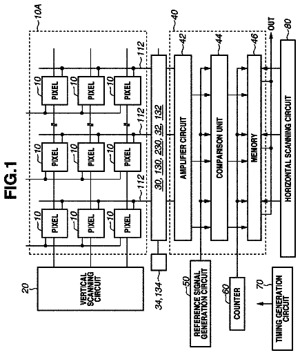
FIG. 2 shows a constitution of the solid-state imaging device 3 . The solid-state imaging device shown in FIG. 2 includes a pixel unit 200 (a pixel array), a vertical scanning circuit 300 , column-processing circuits 350 , a horizontal scanning circuit 400 , an output amplifier 410 , and a control unit 500 . Arrangement positions of circuit elements shown in FIG. 2 may not necessarily coincide with actual arrangement positions.
The pixel unit 200 includes pixels 100 arranged in a two-dimensional matrix form and current sources 130 provided for every column. In the embodiment, a region formed by all pixels of the solid-state imaging device 3 is set as a reading target region of pixel signals, but a part of a region formed by all of the pixels of the solid-state imaging device 3 may be set as the reading target region. The reading target region preferably includes at least all pixels of an effective pixel region. Also, the reading target region may include optical black pixels (pixels from which light is always shielded) disposed outside the effective pixel region. Pixel signals read from the optical black pixels are, for example, used to correct dark current components.
The vertical scanning circuit 300 performs drive control on the pixel unit 200 in units of rows. The vertical scanning circuit 300 is constituted by unit circuits 301 - 1 , 301 - 2 , . . . , and 301 - n (n is the number of rows) equal in number to the rows to perform such drive control.
Each of the unit circuits 301 - i (i=1, 2, . . . , and n) outputs a control signal for controlling the pixels 100 of one row to one of signal lines 110 provided for every row. Each of the signal lines 110 is connected to the pixels 100 and supplies the control signal output from each of the unit circuits 301 - i to the pixels 100 . In FIG. 2 , each of the signal lines 110 corresponding to each row is expressed by one line, but each of the signal lines 110 includes a plurality of signal lines. Signals of the pixels 100 of the row selected by the control signal are output to each of vertical signal lines 120 provided for every column.
The current sources 130 are connected to the vertical signal lines 120 and constitute source follower circuits with amplifier transistors (second amplifier transistors 241 to be described below) in the pixels 100 . Column-processing circuits 350 perform signal processing such as noise suppression on pixel signals output to the vertical signal lines 120 . The horizontal scanning circuit 400 chronologically outputs pixel signals of the pixels 100 of one row output to the vertical signal lines 120 and processed by the column-processing circuits 350 to an output amplifier 410 . The output amplifier 410 amplifies the pixel signals output from the horizontal scanning circuit 400 and outputs the amplified pixel signals to the outside of the solid-state imaging device 3 as image signals. The control unit 500 controls the vertical scanning circuit 300 , the column-processing circuits 350 , and the horizontal scanning circuit 400 to control reading of the pixel signals.
FIG. 3 shows a cross-sectional structure of the solid-state imaging device 3 . The solid-state imaging device 3 has a structure in which two substrates (a first substrate 20 and a second substrate 21 ), in which circuit elements (photoelectric conversion elements, transistors, capacitors, etc.) constituting the pixels 100 are arranged, overlap with each other. The circuit elements constituting the pixels 100 are distributed and disposed on the first substrate 20 and the second substrate 21 . The first substrate 20 and the second substrate 21 are electrically connected to each other such that electrical signals can be exchanged between the two substrates when the pixels 100 are driven.
Photoelectric conversion elements are formed on a main surface side of a side irradiated with light L between two main surfaces (surfaces having a relatively larger surface area than lateral surfaces) of the first substrate 20 , and the light radiated to the first substrate 20 is incident on the photoelectric conversion elements. Connection sections 250 for connecting with the second substrate 21 are formed on a main surface of a side opposite to the main surface of the side irradiated with the light L between the two main surfaces of the first substrate 20 . Signals based on signal charges generated by the photoelectric conversion elements disposed in the first substrate 20 are output to the second substrate 21 via each of the connection sections 250 . In the example shown in FIG. 3 , areas of the main surfaces of the first substrate 20 and the second substrate 21 differ from each other, but the areas of the main surfaces of the first substrate 20 and the second substrate 21 may be the same.
Components other than the pixels 100 , i.e., the vertical scanning circuit 300 , the column-processing circuits 350 , the horizontal scanning circuit 400 , the output amplifier 410 , and the control unit 500 , may be disposed on either the first substrate 20 or the second substrate 21 . Also, circuit elements constituting each of the vertical scanning circuit 300 , the column-processing circuits 350 , the horizontal scanning circuit 400 , the output amplifier 410 , and the control unit 500 may be distributed and disposed on the first substrate 20 and the second substrate 21 .
FIG. 4 shows a circuit constitution of pixel cells constituted by four of the pixels 100 . In the embodiment, a case in which some circuit elements are shared by the four pixels arranged in a vertical direction will be described. The pixel cells constituted by the four pixels 100 include photoelectric conversion elements 201 , 202 , 203 , and 204 , transfer transistors 211 , 212 , 213 , and 214 , a charge-holding unit 230 (floating diffusion), a first reset transistor 220 , a first amplifier transistor 240 , a current source 280 , a clamp capacitor 260 , a sample and hold transistor 270 , a second reset transistor 221 , a sample and hold capacitor 231 , a second amplifier transistor 241 , a first selection transistor 291 , and a second selection transistor 292 . Arrangement positions of circuit elements shown in FIG. 4 may not necessarily coincide with actual arrangement positions.
The circuit elements of the four pixels 100 are included in the pixel cells. A first pixel includes the photoelectric conversion element 201 , the transfer transistor 211 , the charge-holding unit 230 , the first reset transistor 220 , the first amplifier transistor 240 , the current source 280 , the clamp capacitor 260 , the sample and hold transistor 270 , the second reset transistor 221 , the sample and hold capacitor 231 , the second amplifier transistor 241 , the first selection transistor 291 , and the second selection transistor 292 . A second pixel includes the photoelectric conversion element 202 , the transfer transistor 212 , the charge-holding unit 230 , the first reset transistor 220 , the first amplifier transistor 240 , the current source 280 , the clamp capacitor 260 , the sample and hold transistor 270 , the second reset transistor 221 , the sample and hold capacitor 231 , the second amplifier transistor 241 , the first selection transistor 291 , and the second selection transistor 292 .
A third pixel includes the photoelectric conversion element 203 , the transfer transistor 213 , the charge-holding unit 230 , the first reset transistor 220 , the first amplifier transistor 240 , the current source 280 , the clamp capacitor 260 , the sample and hold transistor 270 , the second reset transistor 221 , the sample and hold capacitor 231 , the second amplifier transistor 241 , the first selection transistor 291 , and the second selection transistor 292 . A fourth pixel includes the photoelectric conversion element 204 , the transfer transistor 214 , the charge-holding unit 230 , the first reset transistor 220 , the first amplifier transistor 240 , the current source 280 , the clamp capacitor 260 , the sample and hold transistor 270 , the second reset transistor 221 , the sample and hold capacitor 231 , the second amplifier transistor 241 , the first selection transistor 291 , and the second selection transistor 292 . The charge-holding unit 230 , the first reset transistor 220 , the first amplifier transistor 240 , the current source 280 , the clamp capacitor 260 , the sample and hold transistor 270 , the second reset transistor 221 , the sample and hold capacitor 231 , the second amplifier transistor 241 , the first selection transistor 291 , and the second selection transistor 292 are shared by the four pixels 100 .
One end of each of the photoelectric conversion elements 201 , 202 , 203 , and 204 is grounded. Drain terminals of the transfer transistors 211 , 212 , 213 , and 214 are connected to the other ends of the photoelectric conversion elements 201 , 202 , 203 , and 204 , respectively. Gate terminals of the transfer transistors 211 , 212 , 213 , and 214 are connected to the vertical scanning circuit 300 , and are supplied with transfer pulses ΦTX 1 - 1 , ΦTX 1 - 2 , ΦTX 1 - 3 , and ΦTX 1 - 4 , respectively.
One end of the charge-holding unit 230 is connected to source terminals of the transfer transistors 211 , 212 , 213 , and 214 , and the other end of the charge-holding unit 230 is grounded. A drain terminal of the first reset transistor 220 is connected to a power supply voltage VDD, and a source terminal of the first reset transistor 220 is connected to the source terminals of the transfer transistors 211 , 212 , 213 , and 214 . A gate terminal of the first reset transistor 220 is connected to the vertical scanning circuit 300 and is supplied with a reset pulse ΦRST 1 .
A drain terminal of the first amplifier transistor 240 is connected to the power supply voltage VDD. A gate terminal serving as an input unit of the first amplifier transistor 240 is connected to the source terminals of the transfer transistors 211 , 212 , 213 , and 214 . One end of the current source 280 is connected to a source terminal of the first amplifier transistor 240 , and the other end of the current source 280 is grounded. As an example, the current source 280 may be constituted by a transistor in which a drain terminal thereof is connected to the source terminal of the first amplifier transistor 240 , a source terminal thereof is grounded, and a gate terminal thereof is connected to the vertical scanning circuit 300 . One end of the clamp capacitor 260 is connected to the source terminal of the first amplifier transistor 240 and the one end of the current source 280 via the connection section 250 .
A drain terminal of the sample and hold transistor 270 is connected to the other end of the clamp capacitor 260 . A gate terminal of the sample and hold transistor 270 is connected to the vertical scanning circuit 300 and is supplied with a sample and hold pulse ΦTX 2 . A drain terminal of the second reset transistor 221 is connected to the power supply voltage VDD, and a source terminal of the second reset transistor 221 is connected to a source terminal of the sample and hold transistor 270 . A gate terminal of the second reset transistor 221 is connected to the vertical scanning circuit 300 and is supplied with a reset pulse ΦRST 2 .
One end of the sample and hold capacitor 231 is connected to the source terminal of the sample and hold transistor 270 , and the other end of the sample and hold capacitor 231 is grounded. A drain terminal of the second amplifier transistor 241 is connected to the power supply voltage VDD. A gate terminal constituting an input unit of the second amplifier transistor 241 is connected to the source terminal of the sample and hold transistor 270 . A drain terminal of the first selection transistor 291 is connected to a source terminal of the second amplifier transistor 241 , and a source terminal of the first selection transistor 291 is connected to the vertical signal lines 120 . A gate terminal of the first selection transistor 291 is connected to the vertical scanning circuit 300 and is supplied with a selection pulse ΦSEL 1 .
A drain terminal of the second selection transistor 292 is connected to the source terminal of the first amplifier transistor 240 and the one end of the current source 280 via the connection section 250 . A source terminal of the second selection transistor 292 is connected to the vertical signal lines 120 . A gate terminal of the second selection transistor 292 is connected to the vertical scanning circuit 300 and is supplied with a selection pulse ΦSEL 2 . Polarities of the above-mentioned transistors may be reversed, and the source terminals and the drain terminals may be opposite to the above.
The photoelectric conversion elements 201 , 202 , 203 , and 204 are, for example, photodiodes, generate (produce) signal charges based on an amount of incident light, and hold and store the generated (produced) signal charges. The transfer transistors 211 , 212 , 213 , and 214 are transistors which transfer the signal charges stored in the photoelectric conversion elements 201 , 202 , 203 , and 204 to the charge-holding unit 230 . On/off of the transfer transistors 211 , 212 , 213 , and 214 is controlled by the transfer pulses ΦTX 1 - 1 , ΦTX 1 - 2 , ΦTX 1 - 3 , and ΦTX 1 - 4 from the vertical scanning circuit 300 , respectively. The charge-holding unit 230 is a floating diffusion capacitor which temporarily holds and stores the signal charges transferred from the photoelectric conversion elements 201 , 202 , 203 , and 204 .
The first reset transistor 220 is a transistor which resets the charge-holding unit 230 . On/off of the first reset transistor 220 is controlled by the reset pulse ΦRST 1 from the vertical scanning circuit 300 . The first reset transistor 220 and the transfer transistors 211 , 212 , 213 , and 214 are simultaneously turned on so that the photoelectric conversion elements 201 , 202 , 203 , and 204 can also be reset. The reset of the charge-holding unit 230 /the photoelectric conversion elements 201 , 202 , 203 , and 204 means that the amount of charge stored in the charge-holding unit 230 /the photoelectric conversion elements 201 , 202 , 203 , and 204 is controlled to set states (potentials) of the charge-holding unit 230 /the photoelectric conversion elements 201 , 202 , 203 , and 204 to reference states (reference potentials or reset levels).
The first amplifier transistor 240 is a transistor which outputs amplified signals obtained by amplifying signals based on the signal charges stored in the charge-holding unit 230 , which are input to its gate terminal, from its source terminal. The current source 280 functions as a load of the first amplifier transistor 240 and supplies a current driving the first amplifier transistor 240 to the first amplifier transistor 240 . The first amplifier transistor 240 and the current source 280 constitute a source follower circuit.
The clamp capacitor 260 is a capacitor which clamps (fixes) a voltage level of the amplified signal output from the first amplifier transistor 240 . The sample and hold transistor 270 is a transistor which samples and holds a voltage level of the other end of the clamp capacitor 260 and stores a signal charge in the sample and hold capacitor 231 . On/off of the sample and hold transistor 270 is controlled by the sample and hold pulse ΦTX 2 from the vertical scanning circuit 300 .
The second reset transistor 221 is a transistor which resets the sample and hold capacitor 231 . On/off of the second reset transistor 221 is controlled by the reset pulse ΦRST 2 from the vertical scanning circuit 300 . The reset of the sample and hold capacitor 231 means that the amount of charge stored in the sample and hold capacitor 231 is controlled to set a state (a potential) of the sample and hold capacitor 231 to a reference state (a reference potential or a reset level). The sample and hold capacitor 231 holds and stores signal charges based on analog signals sampled and held by the sample and hold transistor 270 .
Capacitance of the sample and hold capacitor 231 is set to larger capacitance than the charge-holding unit 230 . A metal insulator metal (MIM) capacitor serving as a capacitor with a small leakage current (dark current) per unit area is more preferably used for the sample and hold capacitor 231 . Thus, noise resistance is improved, and a high-quality signal is acquired.
The second amplifier transistor 241 is a transistor which outputs amplified signals obtained by amplifying signals based on the signal charges stored in the sample and hold capacitor 231 , which are input to its gate terminal, from its source terminal. The second amplifier transistor 241 and the current source 130 , which is connected to the vertical signal line 120 , constitute a source follower circuit. The first selection transistor 291 is a transistor which selects the pixels 100 and transmits an output of the second amplifier transistor 241 to the vertical signal line 120 . On/off of the first selection transistor 291 is controlled by the selection pulse ΦSEL 1 from the vertical scanning circuit 300 . The second selection transistor 292 is a transistor which selects the pixels 100 and transmits an output of the first amplifier transistor 240 to the vertical signal line 120 . On/off of the second selection transistor 292 is controlled by the selection pulse ΦSEL 2 from the vertical scanning circuit 300 .
The photoelectric conversion elements 201 , 202 , 203 , and 204 , the transfer transistors 211 , 212 , 213 , and 214 , the charge-holding unit 230 , the first reset transistor 220 , the first amplifier transistor 240 , and the current source 280 among the circuit elements shown in FIG. 4 are disposed on the first substrate 20 . Also, the clamp capacitor 260 , the sample and hold transistor 270 , the second reset transistor 221 , the sample and hold capacitor 231 , the second amplifier transistor 241 , the first selection transistor 291 , and the second selection transistor 292 are disposed on the second substrate 21 .
The connection section 250 is disposed between the first substrate 20 and the second substrate 21 . The amplified signals output from the first amplifier transistor 240 of the first substrate 20 are output to the second substrate 21 via the connection section 250 .
In FIG. 4 , the connection section 250 is disposed on a path of the source terminal of the first amplifier transistor 240 and the one end of the current source 280 with the one end of the clamp capacitor 260 and the drain terminal of the second selection transistor 292 , but is not limited thereto. The connection section 250 may be disposed on paths which are electrically connected from the transfer transistors 211 , 212 , 213 , and 214 to the sample and hold capacitor 231 .
For example, the connection section 250 may be disposed on a path of the source terminals of the transfer transistors 211 , 212 , 213 , and 214 with the one end of the charge-holding unit 230 , the source terminal of the first reset transistor 220 , and the gate terminal of the first amplifier transistor 240 . Alternatively, the connection section 250 may be disposed on a path between the other end of the clamp capacitor 260 and the drain terminal of the sample and hold transistor 270 . In this case, another connection section is disposed on a path of the source terminal of the first amplifier transistor 240 , the one end of the current source 280 , and the one end of the clamp capacitor 260 with the drain terminal of the second selection transistor 292 .
Alternatively, the connection section 250 may be disposed on a path of the source terminal of the sample and hold transistor 270 with the one end of the sample and hold capacitor 231 , the source terminal of the second reset transistor 221 , and the gate terminal of the second amplifier transistor 241 . In this case, another connection section is disposed on a path of the source terminal of the first amplifier transistor 240 , the one end of the current source 280 , and the one end of the clamp capacitor 260 with the drain terminal of the second selection transistor 292 . Therefore, the first reset transistor 220 , the charge-holding unit 230 , the first amplifier transistor 240 , the current source 280 , the clamp capacitor 260 , and the sample and hold transistor 270 among the circuit elements shown in FIG. 4 are disposed on the first substrate 20 or the second substrate 21 .
The description continues in the full USPTO document.
 Lapsed, fee not paid9 drawings