Background
Technical Field
The present disclosure relates to an imaging device and an imaging system.
Description of the Related Art
Imaging devices capable of performing both focus detection and image capturing have been proposed. According to Japanese Patent Laid-Open No. 2013-106194, each pixel of an imaging device includes a first photoelectric conversion portion and a second photoelectric conversion portion. The first and second photoelectric conversion portions are each disposed to be substantially conjugate to the pupil of the lens. During focus detection, signals are read out independently from the first and second photoelectric conversion portions of a plurality of pixels, and two images are formed based on rays that have passed through different positions of the pupil of the lens. An image of a subject can be obtained (captured) by adding the signals from the first and second photoelectric conversion portions together.
Japanese Patent Laid-Open No. 2013-106194 also discloses an imaging device that includes a common amplifier for each pair of the first photoelectric conversion portion and the second photoelectric conversion portion. Specifically, a configuration of such an imaging device for outputting a signal based on a charge in the first photoelectric conversion portion and an added signal obtained by adding charges in the first and second photoelectric conversion portions is disclosed.
Summary
An aspect of the present invention provides an imaging device including a pixel and a control unit. The pixel includes a first photoelectric conversion portion including a first semiconductor region configured to accumulate a signal charge, a second photoelectric conversion portion including a second semiconductor region configured to accumulate a signal charge, a charge holding portion, a first transfer transistor configured to transfer a signal charge in the first photoelectric conversion portion to the charge holding portion, and a second transfer transistor configured to transfer a signal charge in the second photoelectric conversion portion to the charge holding portion. The control unit is configured to perform a first control operation to set the first transfer transistor to be on while keeping the second transfer transistor off from a state where both the first transfer transistor and the second transfer transistor are off, and after performing the first control operation, a second control operation to set a state in which both of the first transfer transistor and the second transfer transistor are on. An impurity concentration of the first semiconductor region is lower than an impurity concentration of the second semiconductor region.
Another aspect of the present invention provides an imaging device including a pixel and a control unit. The pixel includes a first photoelectric conversion portion, a second photoelectric conversion portion, a charge holding portion, a first transfer transistor configured to transfer a signal charge in the first photoelectric conversion portion to the charge holding portion, and a second transfer transistor configured to transfer a signal charge in the second photoelectric conversion portion to the charge holding portion. The control unit is configured to perform a first control operation to set the first transfer transistor to be on while keeping the second transfer transistor off from a state where both the first transfer transistor and the second transfer transistor are off, and after performing the first control operation, a second control operation to set a state in which both of the first transfer transistor and the second transfer transistor are on. For a signal charge, a potential of the first photoelectric conversion portion is higher than a potential of the second photoelectric conversion portion.
Another aspect of the present invention provides an imaging device including a pixel and a lens provided correspondingly to the pixel. The pixel includes a first photoelectric conversion portion including a first semiconductor region configured to accumulate a signal charge, a second photoelectric conversion portion including a second semiconductor region configured to accumulate a signal charge, a charge holding portion, a first transfer transistor configured to transfer a signal charge in the first photoelectric conversion portion to the charge holding portion, and a second transfer transistor configured to be controlled independently from the first transfer transistor and configured to transfer a signal charge in the second photoelectric conversion portion to the charge holding portion. An impurity concentration of the first semiconductor region is lower than an impurity concentration of the second semiconductor region.
Further features of the present invention will become apparent from the following description of exemplary embodiments with reference to the attached drawings.
Brief description of the drawings
FIG. 1 is a diagram illustrating an equivalent circuit of an imaging device.
FIG. 2 is a diagram illustrating an equivalent circuit of the imaging device.
FIG. 3 is a plan view schematically illustrating a structure of the imaging device.
FIG. 4 is a chart illustrating driving timings of the imaging device.
FIG. 5 is a chart illustrating driving timings of the imaging device.
FIGS. 6A and 6B are diagrams schematically illustrating the potential in the imaging device.
FIGS. 7A to 7C are diagrams schematically illustrating a cross-sectional structure of the imaging device.
FIGS. 8A to 8C are diagrams schematically illustrating a cross-sectional structure of the imaging device.
FIGS. 9A to 9D are diagrams schematically illustrating a cross-sectional structure of the imaging device.
FIG. 10 is a block diagram illustrating an imaging system according to an exemplary embodiment.
Description of the embodiments
According to some embodiments, both the saturation charge quantity of a pixel and the accuracy of focus detection are increased.
An increase in the maximum charge quantity which a pixel of imaging devices can handle, namely, the saturation charge quantity of a pixel, is desired. However, inventors have found that increasing the saturation charge quantity of a pixel may cause a residual charge that is left without being transferred. In particular, a residual charge is likely to be caused when a charge in one of photoelectric conversion portions is transferred for focus detection. As a result, the accuracy of focus detection undesirably decreases at a low illuminance.
In view of such issues, embodiments of the present invention allow imaging devices to have both an increased saturation charge quantity of a pixel and an increased accuracy of focus detection.
One embodiment of the present invention provides an imaging device. Each pixel included in the imaging device includes a first photoelectric conversion portion, a second photoelectric conversion portion, a first transfer transistor, a second transfer transistor, and a charge holding portion. An example case will be described herein where the charge holding unit includes a floating diffusion (hereinafter, abbreviated as FD) portion that is electrically connected to an input node of an amplifying portion. The first transfer transistor transfers a signal charge in the first photoelectric conversion portion to the FD portion. The second transfer transistor transfers a signal charge in the second photoelectric conversion portion to the FD portion. FIG. 3 illustrates a first photoelectric conversion portion 101 A, a second photoelectric conversion portion 102 A, a gate electrode of a first transfer transistor 103 A, and a gate electrode of a second transfer transistor 104 A. FIG. 3 also illustrates a first FD region 107 A and a second FD region 108 A that form the FD portion, and a conductive member 109 A that electrically connects the first FD region 107 A and the second FD region 108 A to each other.
In some embodiments, the first photoelectric conversion portion includes a first semiconductor region configured to accumulate a signal charge, and the second photoelectric conversion portion includes a second semiconductor region configured to accumulate a signal charge. An impurity concentration of the first semiconductor region is lower than an impurity concentration of the second semiconductor region.
From another viewpoint, for a signal charge, a potential at the first photoelectric conversion portion is higher than a potential at the second photoelectric conversion portion. In the case where electrons serve as a signal charge, the state where a potential is high for a signal charge is the same as the state where voltage is low. In the case where holes serve as a signal charge, the state where a potential is high for a signal charge is the same as the state where voltage is high. In addition, a potential at a photoelectric conversion portion is a potential at a signal-charge accumulating semiconductor region of the photoelectric conversion portion when the entire semiconductor region is depleted, in a state where a voltage for switching on a transfer transistor is applied to the gate of the transfer transistor.
With such a configuration, firstly, a charge in the first photoelectric conversion portion is transferred to the FD portion. Then, two transfer transistors, each for a corresponding one of the first and second photoelectric conversion portions, are both switched on. Switching on both the two transfer transistors indicates that there is a period for which both the two transfer transistors are switched on. The two transfer transistors need not be switched from off to on at an identical timing. In addition, the two transfer transistors need not be switched from on to off at an identical timing. Switching off both the two transfer transistors indicates that there is a period for which both the two transfer transistors are switched off.
Specifically, an imaging device according to some embodiments includes a control unit configured to perform control to switch on or off the transfer transistors. The control unit performs a first control operation to set the first transfer transistor to be on while keeping the second transfer transistor off from a state where both the first and second transfer transistors are off. By the first control operation, a signal charge in the first photoelectric conversion portion is transferred to the FD portion. The control unit then performs a second control operation to set a state in which both of the first and second transfer transistors are on.
The control unit includes, for example, circuits such as a shift register and a decoder. In such a case, the first and second control operations include outputting a driving pulse for switching on or off a corresponding transfer transistor. In addition to the aforementioned configuration, various circuits that enable control of the transfer transistors are used in the control unit.
The second control operation may be performed in a state where at least part of the signal charge transferred by the first control operation is held in the FD portion. Such a control allows a first signal based on a charge in one of two photoelectric conversion portions to be read out and then an added signal based on the sum of charges in the two photoelectric conversion portions to be read out. In addition, a second signal based on a charge in the other photoelectric conversion portion can be obtained by subtraction processing on the first signal that has been read out first and the added signal.
In some embodiments, voltage at the FD portion is reset between the first control operation and the second control operation. Such a control allows a first signal based on a charge in one of two photoelectric conversion portions and a second signal based on a charge in the other photoelectric conversion portion to be read out independently.
Benefits of the above-described embodiments will be described. A potential at the first photoelectric conversion portion is higher than a potential at the second photoelectric conversion portion or an impurity concentration of a first semiconductor region included in the first photoelectric conversion portion is lower than an impurity concentration of a second semiconductor region included in the second photoelectric conversion portion. Such a configuration can reduce the amount of residual charge or make the amount of residual charge zero during the first control operation in which a charge in the first photoelectric conversion portion is transferred.
The potential at the second photoelectric conversion portion is relatively low in a depleted state or the impurity concentration of the second semiconductor region included in the second photoelectric conversion portion is relatively high. This configuration allows the second photoelectric conversion portion to have an increased saturation charge quantity. In addition, a charge is transferred from the second photoelectric conversion portion by the second control operation in which both the two transfer transistors are switched on. These configurations can reduce the amount of residual charge or make the amount of residual charge zero even if the potential at the second photoelectric conversion portion is relatively low.
As described above, according to some embodiments, both the saturation charge quantity of a pixel and the accuracy of focus detection are increased.
Exemplary embodiments of the present invention will be described in detail below with reference to the accompanying drawings. Note that the present invention is not limited to the exemplary embodiments described below. Modifications obtained by changing part of configurations of the exemplary embodiments described below within the scope not departing from the gist of the present invention should also be construed as embodiments of the present invention. In addition, exemplary embodiments obtained by adding part of configurations of any of the following exemplary embodiments to the other exemplary embodiments or by replacing part of configurations of any of the following exemplary embodiments with part of configurations of the other exemplary embodiments should also be construed as embodiments of the present invention. First Exemplary Embodiment
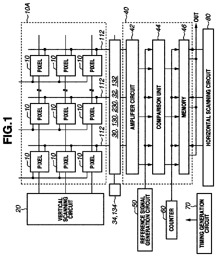
FIG. 1 is a diagram illustrating an equivalent circuit of an imaging device according to a first exemplary embodiment. Each pixel 100 includes a plurality of photoelectric conversion portions. Specifically, referring to FIG. 1 , each pixel 100 includes the first photoelectric conversion portion 101 A and the second photoelectric conversion portion 102 A. For example, photodiodes can be used as the photoelectric conversion portions.
The first transfer transistor 103 A and the second transfer transistor 104 A are each provided for a corresponding one of the plurality of photoelectric conversion portions. The first transfer transistor 103 A and the second transfer transistor 104 A each transfer a charge in the corresponding photoelectric conversion portion to an FD portion 110 . The FD portion 110 serves as an input node of an amplifying portion 201 . In the first exemplary embodiment, the FD portion 110 is included in a charge holding portion. The amplifying portion 201 outputs a signal based on the charge transferred to the FD portion 110 to an output line 207 . A metal oxide semiconductor (MOS) transistor can be used as the amplifying portion 201 . A reset transistor 202 supplies the input node of the amplifying portion 201 with a reset voltage. A selection transistor 203 controls electrical conduction between the amplifying portion 201 and the output line 207 . The output line 207 is electrically connected to a current source 208 . The current source 208 supplies the amplifying portion 201 with a bias current. The amplifying portion 201 and the current source 208 form a source-follower circuit.
Gates of the first transfer transistor 103 A, the second transfer transistor 104 A, the reset transistor 202 , and the selection transistor 203 are connected respectively to driving lines 211 A, 212 A, 209 , and 210 and are sequentially or randomly supplied with a driving pulse from a vertical scanning circuit 112 on a row-by-row basis. In the first exemplary embodiment, the vertical scanning circuit 112 serves as a control unit.
A column circuit 113 receives a signal from the output line 207 . The column circuit 113 is connected directly or via a switch to the output line 207 . The signal processed by the column circuit 113 is sequentially output by a horizontal scanning circuit 114 to an output amplifier 115 and ultimately to outside the imaging device.
The column circuit 113 operates mainly to inversely amplifying the signal supplied from the output line 207 at a gain which is determined based on a capacitance value of an input capacitor 116 and a capacitance value of a feedback capacitor 117 . The column circuit 113 is capable of performing a virtually grounded operation and a correlated double sampling (CDS) operation by a clamping operation using the input capacitor 116 .
Now, an example of specific circuitry of the column circuit 113 will be described. A first node of the input capacitor 116 is electrically connected to the output line 207 . A second node of the input capacitor 116 is electrically connected to an inverting input node of an operational amplifier 119 . A first node of the feedback capacitor 117 is electrically connected to the inverting input node of the operational amplifier 119 and to the second node of the input capacitor 116 . A second node of the feedback capacitor 117 is electrically connected to an output node of the operational amplifier 119 . A switch 118 is provided in a feedback path between the inverting input node and the output node of the operational amplifier 119 in order to control an electrical connection therebetween. The feedback capacitor 117 and the switch 118 are connected in parallel to each other.
A power source 120 supplies a reference voltage Vref to a non-inverting input node of the operational amplifier 119 . Holding capacitors 121 , 122 , 123 , and 124 are capacitors that hold an output from the operational amplifier 119 . Switches 125 , 126 , 127 , to 128 are respectively provided in electrical paths between the operational amplifier 119 and the holding capacitors 121 , 122 , 123 , and 124 and respectively control electrical conduction between the output node of the operational amplifier 119 and the holding capacitors 121 , 122 , 123 , and 124 . Switches 129 , 130 , 131 , and 132 receive signals from the horizontal scanning circuit 114 via signal lines 133 and 134 and cause signals held by the holding capacitors 121 , 122 , 123 , and 124 to be output to horizontal output lines 139 and 140 . The output amplifier 115 outputs a differential signal of the signals output to the horizontal output lines 139 and 140 to outside the imaging device.
A driving pulse PCOR is supplied to the switch 118 . A driving pulse PTN is supplied to the switches 126 and 128 . A driving pulses PISA is supplied to the switch 125 . A driving pulse PTS(A+B) is supplied to the switch 127 .
FIG. 1 illustrates a configuration in which the plurality of pixels 100 each include the amplifying portion 201 ; however, one amplifying portion 201 may be shared by a plurality of pixels, that is, a first pixel 100 A and a second pixel 100 B as illustrated in FIG. 2 . In FIG. 2 , components having functions that are substantially the same as those of components illustrated in FIG. 1 are denoted by the same reference numerals. Different alphabets following a reference numeral indicate that components are included in different pixels.
An imaging device illustrated in FIG. 2 includes the first pixel 100 A which includes the first photoelectric conversion portion 101 A and the second photoelectric conversion portion 102 A, and the second pixel 100 B which includes a first photoelectric conversion portion 101 B and a second photoelectric conversion portion 102 B. Light collected by a first microlens is incident on the first photoelectric conversion portion 101 A and the second photoelectric conversion portion 102 A included in the first pixel 100 A. Light collected by a second microlens is incident on the first photoelectric conversion portion 101 B and the second photoelectric conversion portion 102 B included in the second pixel 100 B.
The first transfer transistors 103 A and 103 B and the second transfer transistors 104 A and 104 B are provided respectively for the first photoelectric conversion portions 101 A and 101 B and the second photoelectric conversion portions 102 A and 102 B. The driving lines 211 A, 211 B, 212 A, and 212 B are provided respectively for the first transfer transistors 103 A and 103 B and the second transfer transistors 104 A and 104 B, as lines that respectively supply driving pulses to the first transfer transistors 103 A and 103 B and the second transfer transistors 104 A and 104 B.
Such a configuration allows a plurality of pixels for imaging capturing to share the amplifying portion 201 , the reset transistor 202 , and the selection transistor 203 . The sharing of components can reduce the number of transistors per pixel and consequently allows larger areas for the photoelectric conversion portions.
The structure of the imaging device according to the first exemplary embodiment in plan view will be described next. FIG. 3 is a plan view schematically illustrating a structure of the imaging device illustrated in FIG. 2 . In FIG. 3 , components corresponding to the components illustrated in FIG. 2 are denoted by the same reference numerals used in FIG. 2 .
The imaging device is formed on a semiconductor substrate, for example, a silicon substrate. The semiconductor substrate includes a plurality of active regions. The first photoelectric conversion portion 101 A and the second photoelectric conversion portion 102 A included in the first pixel 100 A are disposed in a first active region 301 . The first photoelectric conversion portion 101 B and the second photoelectric conversion portion 102 B included in the second pixel 100 B are disposed in a second active region 302 different from the first active region 301 . The first photoelectric conversion portion 101 A includes a first semiconductor region of n-type in which a signal charge accumulates. The second photoelectric conversion portion 102 A includes a second semiconductor region of n-type in which a signal charge accumulates. The first and second semiconductor regions have areas which are substantially equal to each other in plan view.
The first photoelectric conversion portion 101 A and the second photoelectric conversion portion 102 A are disposed so as to be substantially conjugate to the pupil of the lens. The first photoelectric conversion portion 101 A and the second photoelectric conversion portion 102 A receive rays that have passed through different positions of the pupil of the lens. This configuration enables focus detection. An imaging device for focus detection is one of a plurality of embodiments. In other embodiments of the present invention, operations for reading out individual signals and reading out an added signal from the two photoelectric conversion portions may be performed for other usages.
The first active region 301 includes the first FD region 107 A and the second FD region 108 A. A charge in the first photoelectric conversion portion 101 A is transferred to the first FD region 107 A. A charge in the second photoelectric conversion portion 102 A is transferred to the second FD region 108 A. The first FD region 107 A and the second FD region 108 A are electrically connected to each other via contact plugs and the conductive member 109 A. The first FD region 107 A, the second FD region 108 A, and the conductive member 109 A form the FD portion 110 . A figure denoted by the reference numeral 250 represents a contact plug. All the identical figures represent contact plugs; however, illustration of the reference numeral for the other contact plugs is omitted in order to simplify the drawing.
Referring to FIG. 3 , gate electrodes of the individual transistors are denoted by the same reference numerals as those for the corresponding transistors illustrated in FIG. 2 . For example, the gate electrode denoted by 103 A is the gate of the first transfer transistor 103 A illustrated in FIG. 2 . The same applies to the other gate electrodes.
As illustrated in FIG. 3 , the gate electrode of the first transfer transistor 103 A is disposed between the first photoelectric conversion portion 101 A and the first FD region 107 A in plan view. In addition, the gate electrode of the second transfer transistor 104 A is disposed between the second photoelectric conversion portion 102 A and the second FD region 108 A in plan view.
The amplifying portion (hereinafter, also referred to as “amplifying transistor”) 201 , the reset transistor 202 , and the selection transistor 203 are disposed in a third active region 303 different from the first active region 301 and the second active region 302 in which the first photoelectric conversion portion 101 A and the second photoelectric conversion portion 102 A are respectively disposed. Each of these transistors shares a source or drain region with another transistor. Specifically, a drain region shared by the amplifying transistor 201 and the reset transistor 202 is electrically connected via a contact plug to a conductive member 206 which supplies a power source voltage. A source region of the selection transistor 203 is electrically connected via a contact plug to a conductive member that serves as the output line 207 .
In addition, the FD portion 110 is electrically connected to the gate electrode of the amplifying transistor 201 via a contact plug. Specifically, the conductive member 109 A that electrically connects the first FD region 107 A and the second FD region 108 A to each other is electrically connected to the gate electrode of the amplifying transistor 201 via a contact plug. Likewise, a first FD region 107 B and a second FD region 108 B of the second pixel 100 B are also electrically connected to the gate electrode of the amplifying transistor 201 via a conductive member (not illustrated) and contact plugs (not illustrated).
The gate electrode of the first transfer transistor 103 A is electrically connected via a contact plug to a first conductive member 105 A that serves as the corresponding driving line 211 A. The gate electrode of the second transfer transistor 104 A is electrically connected via a contact plug to a second conductive member 106 A that serves as the corresponding driving line 212 A. The gate electrode of the reset transistor 202 is electrically connected via a contact plug to a conductive member 204 that serves as the corresponding driving line 209 . The gate electrode of the selection transistor 203 is electrically connected via a contact plug to a conductive member 205 that serves as the corresponding driving line 210 .
In the first exemplary embodiment, the first conductive members 105 A and 105 B, the second conductive members 106 A and 106 B, and the conductive members 109 A, 109 B, 204 , and 205 are disposed on the same wiring layer; however, any of these conductive members may be disposed on another wiring layer. A wiring layer not illustrated in FIG. 3 includes conductive members that serve as the output line 207 , a power source wiring, and a light-shielding wiring, for example.
As illustrated in FIG. 3 , in the first exemplary embodiment, at least part of an orthogonal projection of the second conductive member 106 A onto a predetermined plane is located between an orthogonal projection of the first conductive member 105 A onto the predetermined plane and an orthogonal projection of the first FD region 107 A or the second FD region 108 A included in the FD portion 110 onto the predetermined plane. The predetermined plane is, for example, a plane that is parallel to an interface between the semiconductor substrate and an insulating film disposed on the semiconductor substrate.
In a modification, at least part of an orthogonal projection of the first conductive member 105 A onto a predetermined plane is located between an orthogonal projection of the second conductive member 106 A onto the predetermined plane and an orthogonal projection of the first FD region 107 A or the second FD region 108 A included in the FD portion 110 onto the predetermined plane. That is, the positions of the first conductive member 105 A and the second conductive member 106 A in FIG. 3 are changed.
Such a structure makes a capacitance component between the first conductive member 105 A and the FD portion 110 smaller than a capacitance component between the second conductive member 106 A and the FD portion 110 . Specifically, in the first exemplary embodiment, a distance over which the first conductive member 105 A, the second conductive member 106 A, and the FD portion 110 extend along one another is about 2.4 micrometers, and a space between wirings of the first conductive member 105 A and the second conductive member 106 A is about 0.3 micrometers. In such a case, the capacitance component between the first conductive member 105 A and the FD portion 110 is approximately half the capacitance component between the second conductive member 106 A and the FD portion 110 . A ratio of the total capacitance component between the first conductive member 105 A and the second conductive member 106 A to the total capacitance of the FD portion 110 is about 20%. Note that the aforementioned numerical values are merely examples and can be changed as appropriate.
In the first exemplary embodiment, the first photoelectric conversion portion 101 A, the gate electrode of the first transfer transistor 103 A, and the first FD region 107 A are arranged along a channel direction of the first transfer transistor 103 A (i.e., along a first direction in FIG. 3 ). In addition, the second photoelectric conversion portion 102 A, the gate electrode of the second transfer transistor 104 A, and the second FD region 108 A are arranged along a channel direction of the second transfer transistor 104 A (i.e., along a third direction in FIG. 3 ). The first conductive member 105 A and the second conductive member 106 A extend along a direction crossing these channel directions (i.e., along a second direction in FIG. 3 ). Such an arrangement enables an efficient arrangement of driving lines for the transfer transistors, leading to larger openings above the photoelectric conversion portions. As a result, the first exemplary embodiment can improve the sensitivity.
In the first exemplary embodiment, an orthogonal projection of the gate electrode of the first transfer transistor 103 A onto a predetermined plane is at least partially superimposed with orthogonal projections of the first conductive member 105 A and the second conductive member 106 A onto the predetermined plane. In addition, an orthogonal projection of the gate electrode of the second transfer transistor 104 A onto a predetermined plane is at least partially superimposed with orthogonal projections of the first conductive member 105 A and the second conductive member 106 A onto the predetermined plane. Such an arrangement enables an efficient arrangement of driving lines for the transfer transistors, leading to larger openings above the photoelectric conversion portions. As a result, the first exemplary embodiment can improve the sensitivity.
Now, how the imaging device according to the first exemplary embodiment is driven will be described with reference to driving pulses illustrated in FIG. 4 . An operation of the imaging device illustrated in FIG. 1 will be described. For each driving pulse, the corresponding transistor is switched on when the driving pulse is at a high level and is switched off when the driving pulse is at a low level.
At time t 1 , driving pulses PTXA and PTXB respectively supplied to the driving lines 211 A and 212 A are switched to the high level. At this time, a driving pulse PRES supplied to the driving line 209 is at the high level. Accordingly, the first photoelectric conversion portion 101 A and the second photoelectric conversion portion 102 A are reset.
At time t 2 , the driving pulses PTXA and PTXB are switched to the low level. At this timing, the first photoelectric conversion portion 101 A and the second photoelectric conversion portion 102 A start accumulating a charge. Because the driving pulse PRES is maintained at the high level, the operation for resetting the FD portion 110 which serves as the input node of the amplifying portion 201 is continued.
At time t 3 , a driving pulse PSEL supplied to the driving line 210 for the selection transistor 203 is switched to the high level, switching on the selection transistor 203 . This consequently causes a signal based on a voltage at the FD portion 110 , that is, a signal based on a voltage at the input node of the amplifying portion 201 , to be output to the output line 207 .
At time t 4 , the driving pulse PRES supplied to the driving line 209 for the reset transistor 202 is switched to the low level to stop the operation for resetting the input node of the amplifying portion 201 . At this time, a signal based on a reset state of the FD portion 110 (hereinafter, referred to as a reset level signal) is output. The reset level signal output to the output line 207 is input to the column circuit 113 . At this time, the operational amplifier 119 of the column circuit 113 is in a virtually grounded state. Specifically, the driving pulse PCOR is at the high level, and the switch 118 is in the conducting state. The operational amplifier 119 is buffering an output of the reference voltage Vref. In this state, the input capacitor 116 is supplied with the reset level signal.
At time t 5 , the driving pulse PCOR is switched to the low level. At time t 6 , the driving pulse PTN is switched from the low level to the high level to switch on the switches 126 and 128 . At time t 7 , the driving pulse PTN is switched from the high level to the low level to switch off the switches 126 and 128 . This operation causes an output substantially equal to the reference voltage Vref to be held by the holding capacitors 122 and 124 as the reset level signal.
At time t 8 , the driving pulse PTXA is switched to the high level. At time t 9 , the driving pulse PTXA is switched to the low level. This operation causes a charge in the first photoelectric conversion portion 101 A to be transferred to the FD portion 110 . Consequently, a first signal based on the charge generated by the first photoelectric conversion portion 101 A is supplied to the column circuit 113 via the amplifying portion 201 and the output line 207 . The first signal can be used for focus detection.
Because the driving pulse PTXB is maintained at the low level from time t 8 to time t 9 , the second transfer transistor 104 A is switched off. Specifically, at time t 8 , the first transfer transistor 103 A is switched on while keeping the second transfer transistor 104 A switched off, from the state where both the first transfer transistor 103 A and the second transfer transistor 104 A are switched off.
The column circuit 113 outputs a value obtained by multiplying a change in voltage by an inverting gain which is a ratio between a capacitance value C0 of the input capacitor 116 and a capacitance value Cf of the feedback capacitor 117 . Here, let ΔVa (a negative value) denote a change in voltage at the output line 207 . Then, an output voltage V(A) of the operational amplifier 119 is denoted by Equation (1). V ( A )= V ref+Δ Va ×(− C 0/ Cf ) Equation
At time t 10 , the driving pulse PTSA is switched from the low level to the high level to switch on the switch 125 . At time t 11 , the driving pulse PTSA is switched from the high level to the low level to switch off the switch 125 . This operation causes the output voltage V(A) of the operational amplifier 119 to be held in the holding capacitor 121 . The signal held by the holding capacitor 121 corresponds to the first signal output from the first photoelectric conversion portion 101 A for focus detection.
At time t 12 , the driving pulse PTXA is switched to the high level. The driving pulse PTXB is switched to the high level for at least a period within a period for which the driving pulse PTXA is at the high level. This consequently switches on both the first transfer transistor 103 A and the second transfer transistor 104 A. This operation allows charges in both the first photoelectric conversion portion 101 A and the second photoelectric conversion portion 102 A to be simultaneously transferred to the FD portion 110 . Note that the driving pulses PTXA and PTXB may be simultaneously switched from the low level to the high level. Alternatively, the driving pulse PTXA may be switched from the low level to the high level before or after the driving pulse PTXB is switched from the low level to the high level.
The operation from time t 12 to time t 13 enables generation of an image formation signal at the output line 207 . The image formation signal at the output line 207 is supplied to the column circuit 113 . Let ΔVa+b (a negative value) denote a change in voltage at the output line 207 . Then, an output voltage V(A+B) of the operational amplifier 119 is denoted by Equation (2). V ( A+B )= V ref+Δ Va+b ×(− C 0/ Cf ) Equation
At time t 14 , the driving pulse PTS(A+B) is switched from the low level to the high level to switch on the switch 127 . At time t 15 , the driving pulse PTS(A+B) is switched from the high level to the low level to switch off the switch 127 . This operation causes the voltage V(A+B) at the output node of the operational amplifier 119 to be held in the holding capacitor 123 . The signal held by the holding capacitor 123 corresponds to the image formation signal.
At time t 16 , the driving pulse PRES is switched to the high level. This consequently switches on the reset transistor 202 , and the voltage at the FD portion 110 is reset.
The switches 129 to 132 sequentially conduct in synchronization with a pulse PH at and after time t 17 . This causes the signals held by the holding capacitors 121 to 124 to be sequentially read out to the horizontal output lines 139 and 140 .
An image formation signal for one pixel is obtained based on a difference between voltages at the holding capacitors 123 and 124 . The difference is denoted by Equation (3). V ( A+B )− V ref=Δ Va+b ×(− C 0/ Cf ) Equation
In addition, a signal of the first photoelectric conversion portion 101 A alone is obtained based on a difference between voltages at the holding capacitors 121 and 122 . The difference is denoted by Equation (4). V ( A )− V ref=Δ Va ×(− C 0/ Cf ) Equation
Further, a signal of the second photoelectric conversion portion 102 A alone is obtained based on a difference between voltages at the holding capacitors 121 and 123 . The difference is denoted by Equation (5). V ( A+B )− V ( A )=(Δ Va+b−ΔVa )×(− C 0/ Cf ) Equation
The calculations described above can be performed by the imaging device or by a signal processor after the signals are output from the imaging device. However, the signal of the first photoelectric conversion portion 101 A alone and the added signal of the signals of the first photoelectric conversion portion 101 A and the second photoelectric conversion portion 102 A are obtained by the imaging device.
The description continues in the full USPTO document.
 Lapsed, fee not paid4 drawings