Cross-reference to related applications
This application is a national stage application (under 35 U.S.C. §371) of PCT/EP2013/003694, filed Dec. 6, 2013, which claims benefit of European Application No. 12008649.1, filed Dec. 28, 2012, both of which are incorporated herein by reference in their entirety.
Field of the invention
The present invention relates to novel compositions comprising one or more polymeric organic semiconducting compounds (OSC) and one or more organic solvents, to their use as conducting inks for the preparation of organic electronic (OE) devices, especially organic photovoltaic (OPV) cells and organic light emitting diodes (OLED) devices, to methods for preparing OE devices using the novel compositions, and to OE devices, as well as OPV cells and OLED devices prepared from such methods and compositions.
Background and prior art
When preparing OE devices, especially OLED devices, it is essential to get even film formation, as a 3% variation in film thickness is visible to the naked eye. This is commonly very difficult to achieve. Frequently poor uniformity is seen, this can take the form of coffee staining where the ink is thicker at the edges and thinner in the centre; reticulation where the ink coalesces into large droplets; point defects where small holes appear within the surface of the film. In dual solvent systems Marangoni effects can also been seen.
US 2007/0221885 relates to a three solvent system and is specifically relating to one solvent used to solubilise the active material, a second solvent that has a similar surface energy to the substrate and a third solvent which is used to make the other two solvents miscible. 3,4-dimethylanisole is mentioned within a list of solvents as a potential material to be used, it is not exemplified as one of the solvents. The main drive for this patent is to obtain printability onto low surface energy substrates.
WO 2006/122732 relates to compositions, especially solutions, of at least one organic semiconductor emitting light from the triplet state, in an organic solvent or solvent mixture. The solvent may include 3,4-dimethylanisole. However, no example is provided.
Furthermore WO 2011/076325 A1 describes the use of dimethylanisole as a solvent. However, the solvent is used for small molecules having a molecular weight of at most 5,000 g/mol. No hints regarding OE devices which comprise polymers as OSC materials are provided.
The prior art provides compositions being useful in order to process organic light emitting and charge transporting materials. However, it is a permanent desire to improve the performance of the OE layer, preferably the OLED layer, such as efficiency, lifetime and sensitivity regarding oxidation or water.
In addition thereto, the formulation should enable a low-cost and easy printing process. The printing process should allow a high quality printing at high speed.
It is therefore desirable to have improved formulations comprising an OSC that are suitable for the preparation of OE devices, especially thin film transistors, diodes, OLED displays and OPV cells, which allow the manufacture of high efficient OE devices having a high performance, a long lifetime and a low sensitivity against water and/or oxidation. One aim of the present invention is to provide such improved formulations. Another aim is to provide improved methods of preparing an OE device from such formulations. Another aim is to provide improved OE devices obtained from such formulations and methods. Further aims are immediately evident to the person skilled in the art from the following description.
Surprisingly it has been found that these aims can be achieved, and the above-mentioned problems can be solved, by providing methods, materials and devices as claimed in the present invention, especially by providing a process for preparing an OE device using a formulation of the present invention.
Summary of the invention
The invention relates to a composition comprising one or more organic semiconducting compounds (OSC) having a molecular weight of at least 10,000 g/mol, and one or more organic solvents, characterized in that said organic solvent comprises a mono- or di-(C.sub.1-C.sub.5-alkyl)anisole, preferably a di(C.sub.1-C.sub.3-alkyl)anisole, more preferably a dimethylanisole and most preferably 3,4-dimethylanisole.
The invention further relates to the use of a composition as described above and below as coating or printing ink for the preparation of OE devices, preferably OLED devices, in particular for rigid and flexible OLED devices.
The invention further relates to a process of preparing an organic electronic (OE) device, comprising the steps of a) depositing the composition as described above and below onto a substrate to form a film or layer, preferably by coating or printing, more preferably by ink jet printing, flexographic or gravure printing, most preferably by ink jet printing and b) removing the solvent(s).
The invention further relates to an OE device, preferably an OLED device, prepared from a formulation and/or by a process as described above and below.
The OE devices include, without limitation, organic field effect transistors (OFET), integrated circuits (IC), thin film transistors (TFT), Radio Frequency Identification (RFID) tags, organic light emitting diodes (OLED), organic light emitting transistors (OLET), electroluminescent displays, organic photovoltaic (OPV) cells, organic solar cells (O-SC), flexible OPVs and O-SCs, organic laserdiodes (O-laser), organic integrated circuits (O-IC), lighting devices, sensor devices, electrode materials, photoconductors, photodetectors, electrophotographic recording devices, capacitors, charge injection layers, Schottky diodes, planarising layers, antistatic films, conducting substrates, conducting patterns, photoconductors, electrophotographic devices, organic memory devices, biosensors and biochips.
According to a preferred embodiment, the present invention provides organic light emitting diodes (OLED). OLED devices can for example be used for illumination, for medical illumination purposes, as signalling devices, as signage devices, and in displays. Displays can be addressed using passive matrix driving, total matrix addressing or active matrix driving. Transparent OLEDs can be manufactured by using optically transparent electrodes. Flexible OLEDs are assessable through the use of flexible substrates.
The formulations, methods and devices of the present invention provide surprising improvements in the efficiency of the OE devices and the production thereof. Unexpectedly, the performance, the lifetime and the efficiency of the OE devices can be improved, if these devices are achieved by using a composition of the present invention. Furthermore, it was surprisingly found that these formulations are suitable for printing techniques, especially for ink jet, flexographic and gravure printing. Furthermore, the composition of the present invention provides an astonishingly high level of film forming. Especially, the homogeneity and the quality of the films can be improved. In addition thereto, the formulations enable a low-cost and easy printing process. The printing processes allow a high quality printing at high speed.
A brief description of the figures
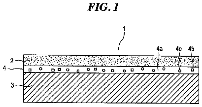
FIG. 1A exemplarily and schematically depicts a typical bottom gate (BG), top contact (TC) OFET device according to the present invention, comprising a substrate ( 1 ), a gate electrode ( 2 ), a layer of dielectric material ( 3 ) (also known as gate insulator layer), an OSC layer ( 4 ), and source and drain (S/D) electrodes ( 5 ), and an optional passivation or protection layer ( 6 ).
FIG. 1B exemplarily and schematically depicts a typical bottom gate (BG), bottom contact (BC) OFET device according to the present invention, comprising a substrate ( 1 ), a gate electrode ( 2 ), a dielectric layer ( 3 ), S/D electrodes ( 5 ), an OSC layer ( 4 ), and an optional passivation or protection layer ( 6 ).
FIG. 2 exemplarily and schematically depicts a top gate (TG) OFET device according to the present invention, comprising a substrate ( 1 ), source and drain electrodes ( 5 ), an OSC layer ( 4 ), a dielectric layer ( 3 ), and a gate electrode ( 2 ), and an optional passivation or protection layer ( 6 ).
FIG. 3 exemplarily and schematically depict typical and preferred OPV devices according to the present invention.
FIG. 4 exemplarily and schematically depict typical and preferred OPV devices according to the present invention.
Detailed description of the invention
The formulation of the present invention comprises at least one polymeric organic semiconducting compound (OSC). The OSC compounds can be selected from standard materials known to the skilled person and described in the literature.
OLEDs which comprise polymers as organic materials are frequently also known as PLEDs (PLED=polymeric light emitting diodes). Their simple production holds the promise of inexpensive production of corresponding electroluminescent devices.
PLEDs consist either only of one layer, which is able to combine as far as possible all functions (charge injection, charge transport, recombination) of an OLED in itself, or they consist of a plurality of layers which comprise the respective functions individually or partially combined. For the preparation of polymers having the corresponding properties, the polymerisation is carried out using different monomers which take on the corresponding functions.
The organic semiconducting compound has a molecular weight of at least 10,000 g/mol, preferably at least 20,000 g/mol, more preferably at least 50,000 g/mol and most preferably at least 100,000 g/mol. Surprising effects can be achieved with organic semiconducting compounds having a molecular weight in the range of 10,000 to 20,000,000 g/mol, preferably in the range of 20,000 to 10,000,000 g/mol, more preferably in the range of 50,000 to 5,000,000 g/mol and most preferably in the range of 100,000 to 2,000,000 g/mol. The molecular weight of the organic semiconducting compound relates to the weight average. The weight average molecular weight M.sub.w can be measured by standard methods such as gel permeation chromatography (GPC) against polystyrene standards.
In the present application, the term “polymer” is taken to mean both polymeric compounds and dendrimers. The polymeric compounds according to the invention preferably have 10 to 10,000, more preferably 20 to 5,000 and in most preferably 50 to 2,000 structural units. The branching factor of the polymers here is between 0 (linear polymer, no branching sites) and 1 (fully branched dendrimer).
In a preferred embodiment of the present invention, the polymers useful for the invention may contain structural units as disclosed and listed extensively in WO 02/077060 A1, in WO 2005/014689 A2 and in WO 2010/136110 A2. These are incorporated into the present application by way of reference. The further structural units can originate, for example, from the following classes: Group 1: Units which influence, preferably enhance, the hole-injection and/or hole-transport properties of the polymers; Group 2: Units which influence, preferably enhance, the electron-injection and/or electron-transport properties of the polymers; Group 3: Units which have combinations of individual units from group 1 and group 2; Group 4: Units which modify the emission characteristics to such an extent that electrophosphorescence can be obtained instead of electrofluorescence; Group 5: Units which improve transfer from the singlet state to the triplet state; Group 6: Units which influence the emission colour of the resultant polymers; Group 7: Units which are typically used as backbone; Group 8: Units which influence the film-morphological and/or rheological properties of the resultant polymers.
Preferred polymers according to the invention are those in which at least one structural unit has charge-transport properties, i.e. which contain units from groups 1 and/or 2.
Structural units from group 1 which have hole-injection and/or hole-transport properties are, for example, triarylamine, benzidine, tetraaryl-para-phenylenediamine, triarylphosphine, phenothiazine, phenoxazine, dihydrophenazine, thianthrene, dibenzo-para-dioxin, phenoxathiyne, carbazole, azulene, thiophene, pyrrole and furan derivatives and further O-, S- or N-containing heterocycles having a high HOMO (HOMO=highest occupied molecular orbital). These arylamines and heterocycles preferably result in an HOMO in the polymer of greater than −5.8 eV (against vacuum level), particularly preferably greater than −5.5 eV.
Structural units from group 2 which have electron-injection and/or electron-transport properties are, for example, pyridine, pyrimidine, pyridazine, pyrazine, oxadiazole, quinoline, quinoxaline, anthracene, benzanthracene, pyrene, perylene, benzimidazole, triazine, ketone, phosphine oxide and phenazine derivatives, but also triarylboranes and further O-, S- or N-containing heterocycles having a low LUMO (LUMO=lowest unoccupied molecular orbital). These units in the polymer preferably result in an LUMO of less than −1.9 eV (against vacuum level), particularly preferably less than −2.5 eV.
It may be preferred for the polymers according to the present invention to contain units from group 3 in which structures which increase the hole mobility and structures which increase the electron mobility (i.e. units from groups 1 and 2) are bonded directly to one another or structures which increase both the hole mobility and the electron mobility. Some of these units can serve as emitters and shift the emission colour into the green, yellow or red. Their use is thus suitable, for example, for the generation of other emission colours from originally blue-emitting polymers.
Structural units from group 4, so-called triplet emitter units, are those which are able to emit light from the triplet state with high efficiency, even at room temperature, i.e. exhibit electrophosphorescence instead of electrofluorescence, which frequently causes an increase in the energy efficiency. For the purposes of the present application, a triplet emitter unit is taken to mean a compound which comprises a triplet emitter. For the purposes of the present application, triplet emitters are taken to mean all compounds which are capable of emitting light in the visible or NIR region through transfer from a triplet state into an energetically lower state. This is also referred to as phosphorescence. Suitable for this purpose are firstly compounds which contain heavy atoms having an atomic number of greater than 36. Preference is given to compounds which contain d- or f-transition metals which satisfy the above-mentioned condition. Particular preference is given here to corresponding structural units which contain elements from groups 8 to 10 (Ru, Os, Rh, Ir, Pd, Pt). Suitable structural units for the polymers according to the invention here are, for example, various complexes, as described, for example, in WO 02/068435 A1, WO 02/081488 A1 and EP 1239526 A2. Corresponding monomers are described in WO 02/068435 A1 and in WO 2005/042548 A1.
It is preferred in accordance with the present invention to employ triplet emitters which emit in the visible spectral region (red, green or blue).
The triplet emitter may be part of the backbone of the polymer (i.e. in the main chain of the polymer) or it may be located in the side chain of the polymer.
Structural units from group 5 are those which improve transfer from the singlet state to the triplet state and which, employed in support of the above-mentioned triplet emitter units, improve the phosphorescence properties of these structural elements. Suitable for this purpose are, in particular, carbazole and bridged carbazole dimer units, as described, for example, in WO 2004/070772 A2 and WO 2004/113468 A1. Also suitable for this purpose are ketones, phosphine oxides, sulfoxides, sulfones, silane derivatives and similar compounds, as described, for example, in WO 2005/040302 A1.
Structural units from group 6, are those which have at least one further aromatic structure or another conjugated structure which does not fall under the above-mentioned groups, i.e. which have only little influence on the charge-carrier mobilities, are not organometallic complexes or do not influence singlet-triplet transfer. Structural elements of this type can influence the emission colour of the resultant polymers. Depending on the unit, they can therefore also be employed as emitters. Preference is given here to aromatic structures having 6 to 40 C atoms and also tolan, stilbene or bisstyrylarylene derivatives, each of which may be substituted by one or more radicals. Particular preference is given here to the incorporation of 1,4-phenylene, 1,4-naphthylene, 1,4- or 9,10-anthrylene, 1,6-, 2,7- or 4,9-pyrenylene, 3,9- or 3,10-perylenylene, 4,4′-biphenylylene, 4,4″-terphenylylene, 4,4′-bi-1,1′-naphthylylene, 4,4′-tolanylene, 4,4′-stilbenylene, 4,4″-bisstyrylarylene, benzothiadiazole and corresponding oxygen derivatives, quinoxaline, phenothiazine, phenoxazine, dihydrophenazine, bis(thiophenyl)arylene, oligo(thiophenylene), phenazine, rubrene, pentacene or perylene derivatives, which are preferably substituted, or preferably conjugated push-pull systems (systems which are substituted by donor and acceptor substituents) or systems such as squarines or quinacridones, which are preferably substituted.
Structural units from group 7 are units which contain aromatic structures having 6 to 40 C atoms, which are typically used as polymer backbone. These are, for example, 4,5-dihydropyrene derivatives, 4,5,9,10-tetrahydropyrene derivatives, fluorene derivatives, 9,9′-spirobifluorene derivatives, phenanthrene derivatives, 9,10-dihydrophenanthrene derivatives, 5,7-dihydrodibenzoxepine derivatives and cis- and trans-indenofluorene derivatives, but in principle also all similar structures which, after polymerisation, would result in a conjugated, bridged or unbridged polyphenylene or polyphenylene-vinylene homopolymer. Here too, the said aromatic structure may contain heteroatoms, such as O, S or N, in the backbone or the side chain.
Structural units from group 8 are those which influence the film-morphological properties and/or the rheological properties of the polymers, such as, for example, siloxanes, long alkyl chains or fluorinated groups, but also particularly rigid or flexible units, such as, for example, liquid crystal-forming units or crosslinkable groups.
The synthesis of the above-described units from groups 1 to 8 and of the further emitting units is known to the person skilled in the art and is described in the literature, for example in WO 2005/014689 A2, WO 2005/030827 A1, WO 2005/030828 A1 and WO 2010/136110 A2. These documents and the literature cited therein are incorporated into the present application by way of reference.
The polymers useful for the present invention may contain one or more units selected from groups 1 to 8. It may furthermore be preferred for more than one structural unit from one group to be present simultaneously.
The way in which white-emitting copolymers can be synthesised is described in detail, for example, in WO 2005/030827 A1, WO 2005/030828 A1 and WO 2010/136110 A2.
Astonishing improvements can be achieved with one or more polymeric organic semiconducting compounds having a high solubility. Preferred polymeric organic semiconducting compounds can comprise Hansen Solubility parameters of H.sub.d in the range of 17.0 to 20.0 MPa.sup.0.5, H.sub.p in the range of 2 to 10.0 MPa.sup.0.5 and H.sub.h in the range of 0.0 to 15.0 MPa.sup.0.5. More preferred organic semiconducting compounds comprise Hansen Solubility parameters of H.sub.d in the range of 17.5 to 19.0 MPa.sup.0.5, H.sub.p in the range of 3.5 to 8.0 MPa.sup.0.5 and H.sub.h in the range of 3.0 to 10.0 MPa.sup.0.5.
Surprising effects can be achieved with organic semiconducting compounds having a radius of at least 3.0 MPa.sup.0.5, preferably at least 4.5 MPa.sup.0.5 and more preferably at least 5.0 MPa.sup.0.5 determined according to Hansen Solubility parameters.
The Hansen Solubility Parameters can be determined according to the Hansen Solubility Parameters in Practice HSPiP 3.sup.rd edition, (Software version 3.0.38) with reference to the Hansen Solubility Parameters: A User's Handbook, Second Edition, C. M. Hansen (2007), Taylor and Francis Group, LLC) as supplied by Hanson and Abbot et al.
The positions H.sub.d, H.sub.p and H.sub.h are the coordinates in 3 dimensional space for the centre of the organic semiconducting compound, whilst the radius, gives the distance that the solubility extends, i.e. if the radius is large it will encompass more solvents that would dissolve the material and conversely if it was small then a restricted number of solvents would solubilise the organic semiconducting compound.
According to a special aspect of the present invention the organic semiconducting compound may comprise a high glass transition temperature. Preferably, the organic semiconducting compound may have a glass transition temperature preferably of at least 70° C., more preferably of at least 100° C. and most preferably of at least 125° C. determined according to DIN 51005.
According to a special embodiment of the present invention, the OSC can be used for example as the active channel material in the semiconducting channel of an OFET, or as a layer element of an organic rectifying diode.
In case of OFET devices, where the OFET layer contains an OSC as the active channel material, it may be an n- or p-type OSC. The semiconducting channel may also be a composite of two or more OSC compounds of the same type, i.e. either n- or p-type. Furthermore, a p-type channel OSC compound may for example be mixed with an n-type OSC compound for the effect of doping the OSC layer. Multilayer semiconductors may also be used. For example, the OSC may be intrinsic near the insulator interface and a highly doped region can additionally be coated next to the intrinsic layer.
Preferred OSC compounds have a FET mobility of greater than 1×10.sup.−5 cm.sup.2V.sup.−1 s.sup.−1, more preferably greater than 1×10.sup.−2 cm.sup.2 V.sup.−1 s.sup.−1.
According to a preferred embodiment of the present invention the OSC material is an organic light emitting material and/or charge transporting material. The organic light emitting materials and charge transporting materials can be selected from standard materials known to the skilled person and described in the literature. Organic light emitting material according to the present application means a material which emits light having a λ.sub.max in the range from 400 to 700 nm.
According to a special embodiment of the present invention, the composition preferably comprises 0.1 to 10% by weight, more preferably 0.25 to 5% and most preferably 0.5 to 4% by weight of organic semiconducting compounds having a molecular weight of at least 10,000 g/mol, preferably emitting materials and/or charge transporting materials.
It may additionally be preferred to use the organic semiconducting compounds (OSC) having a molecular weight of at least 10,000 g/mol not as the pure substance, but instead as a mixture together with further polymeric, oligomeric, dendritic or low-molecular-weight substances of any desired type. These may, for example, improve the electronic properties or themselves emit. Above and below, a mixture is taken to mean a composition which comprises at least one polymeric component.
In a further embodiment of the present invention, it is preferred for a mixture to comprise an organic semiconducting compound (OSC) having a molecular weight of at least 10,000 g/mol and a low-molecular-weight substance. The low-molecular-weight substance is preferably a triplet emitter.
In a further embodiment, it is preferred for the organic semiconducting compounds (OSC) having a molecular weight of at least 10,000 g/mol to be employed in an emitting layer together with an emitting compound having a low molecular weight. In this case, the polymer is preferably employed in combination with one or more phosphorescent materials (triplet emitters). For the purposes of the present application, phosphorescence is taken to mean the luminescence from an excited state of relatively high spin multiplicity, i.e. a spin state>1, in particular from an excited triplet state or from an MLCT mixed state. The mixture comprising the organic semiconducting compounds (OSC) having a molecular weight of at least 10,000 g/mol and the emitting compound then comprises between 99 and 1% by weight, preferably between 98 and 60% by weight, more preferably between 97 and 70% by weight, and most preferably between 95 and 75% by weight, of the organic semiconducting compounds (OSC) having a molecular weight of at least 10000 g/mol, based on the entire mixture comprising emitter and matrix material. Correspondingly, the mixture comprises up to 99% by weight, preferably up to 40% by weight, more preferably up to 30% by weight and most preferably up to 25% by weight, of the emitter, based on the entire mixture comprising emitter and matrix material. In addition, the mixture comprises at least 1% by weight, preferably at least 2% by weight, more preferably at least 3% by weight and most preferably at least 5% by weight, of the emitter, based on the entire mixture comprising emitter and matrix material.
In the above-mentioned embodiment in which the organic semiconducting compounds (OSC) having a molecular weight of at least 10,000 g/mol is employed in an emitting layer together with an emitting compound, the proportion of the emitting compound may, however, also be significantly lower. In this case, the mixture preferably comprises at least 0.01% by weight of the emitter, based on the entire mixture, but preferably less than 5% by weight, more preferably less than 3% by weight and most preferably less than 1.5% by weight of the emitter, based on the entire mixture.
Suitable phosphorescent compounds are, in particular, compounds which emit light, preferably in the visible region, on suitable excitation and in addition contain at least one atom having an atomic number of greater than 36 and less than 84, preferably greater than 56 and less than 80.
Examples of the emitters described above are revealed by the applications WO 00/70655, WO 01/41512, WO 02/02714, WO 02/15645, EP 1191613, EP 1191612, EP 1191614, WO 05/033244 and DE 102008015526. In general, all phosphorescent complexes as used in accordance with the prior art for phosphorescent OLEDs and as are known to the person skilled in the art in the area of organic electroluminescence are suitable, and the person skilled in the art will be able to use further phosphorescent complexes without an inventive step.
In a further embodiment according to the invention, the triplet emitter preferably contains an organometallic connecting unit. The organometallic connecting unit is preferably an organometallic coordination compound. In the present application, an organometallic coordination compound is taken to mean a compound having a metal atom or ion in the centre of the compound surrounded by an organic compound as ligand. In addition, an organometallic coordination compound is characterised in that at least one carbon atom of the ligand is bonded to the central metal via a coordination bond. Electrically neutral triplet emitters are furthermore preferred.
The triplet emitters preferably contain only chelating ligands, i.e. ligands which coordinate to the metal via at least two bonding sites; the use of two or three bidentate ligands, which may be identical or different, is particularly preferred. The preference for chelating ligands is due to the higher stability of chelate complexes.
Particularly preferred organic phosphorescent compounds are compounds of formulae
to (4):
##STR00001## where DCy is, identically or differently on each occurrence, a cyclic group which contains at least one donor atom, preferably nitrogen, carbon in the form of a carbene or phosphorus, via which the cyclic group is bonded to the metal, and which may in turn carry one or more substituents R.sup.1; the groups DCy and CCy are connected to one another via a covalent bond; CCy is, identically or differently on each occurrence, a cyclic group which contains a carbon atom via which the cyclic group is bonded to the metal and which may in turn carry one or more substituents R.sup.1; A is, identically or differently on each occurrence, a monoanionic, bidentate chelating ligand, preferably a diketonate ligand; R.sup.1 are identically or differently at each instance, and are F, Cl, Br, I, NO.sub.2, CN, a straight-chain, branched or cyclic alkyl or alkoxy group having from 1 to 20 carbon atoms, in which one or more nonadjacent CH.sub.2 groups may be replaced by —O—, —S—, —NR.sup.2—, —CONR.sup.2—, —CO—O—, —C═O—, —CH═CH— or —C≡C—, and in which one or more hydrogen atoms may be replaced by F, or an aryl or heteroaryl group which has from 4 to 14 carbon atoms and may be substituted by one or more nonaromatic R.sup.1 radicals, and a plurality of substituents R.sup.1, either on the same ring or on the two different rings, may together in turn form a mono- or polycyclic, aliphatic or aromatic ring system; and R.sup.2 are identically or differently at each instance, and are a straight-chain, branched or cyclic alkyl or alkoxy group having from 1 to 20 carbon atoms, in which one or more nonadjacent CH.sub.2 groups may be replaced by —O—, —S—, —CO—O—, —C═O—, —CH═CH— or —C≡C—, and in which one or more hydrogen atoms may be replaced by F, or an aryl or heteroaryl group which has from 4 to 14 carbon atoms and may be substituted by one or more nonaromatic R.sup.1 radicals.
Formation of ring systems between a plurality of radicals R.sup.1 means that a bridge may also be present between the groups DCy and CCy. Further-more, formation of ring systems between a plurality of radicals R.sup.1 means that a bridge may also be present between two or three ligands CCy-DCy or between one or two ligands CCy-DCy and the ligand A, giving a polydentate or polypodal ligand system.
Examples of the emitters described above are revealed by the applications WO 00/70655, WO 01/41512, WO 02/02714, WO 02/15645, EP 1191613, EP 1191612, EP 1191614, WO 04/081017, WO 05/033244, WO 05/042550, WO 05/113563, WO 06/008069, WO 06/061182, WO 06/081973, DE 102008027005 and WO 2011/076325 A1. In general, all phosphorescent complexes as are used in accordance with the prior art for phosphorescent OLEDs and as are known to the person skilled in the art in the area of organic electroluminescence are suitable, and the person skilled in the art will be able to use further phosphorescent compounds without inventive step. In particular, it is known to the person skilled in the art which phosphorescent complexes emit with which emission colour.
The composition of the present invention comprises a mono- or di-(C.sub.1-C.sub.5-alkyl)anisole, preferably a di-(C.sub.1-C.sub.3-alkyl)anisole, more preferably a dimethylanisole and most preferably 3,4-dimethylanisole.
In addition thereto, the composition may comprise a further solvent. By using an additional solvent an astonishing improvement in solubility can be obtained. Obtaining the correct balance of evaporation rate and boiling point is essential in order to maintain solubility whilst drying. Preferably, tetra methyl benzene, more preferably 1,2,4,5 tetra methyl benzene can be used as additional solvent.
Preferred further organic solvents comprise Hansen Solubility parameters of H.sub.d in the range of 16.0 to 23.2 MPa.sup.0.5, H.sub.p in the range of 0.0 to 12.5 MPa.sup.0.5 and H.sub.h in the range of 0.0 to 14.2 MPa.sup.0.5. More preferred organic solvents comprise Hansen Solubility parameters of H.sub.d in the range of 17.0 to 20.0 MPa.sup.0.5, H.sub.p in the range of 0.0 to 8.0 MPa.sup.0.5 and H.sub.h in the range of 0.0 to 9.0 MPa.sup.0.5.
Preferably the further solvent has a boiling point or sublimation temperature of ≦400° C., preferably ≦300° C., more preferably ≦250° C., and most preferably ≦200° C., at the pressure employed, very preferably at atmospheric pressure (1013 hPa). Evaporation can also be accelerated e.g. by applying heat and/or reduced pressure. Unexpected improvements can be achieved by using solvents having a boiling point of at least 100° C., preferably at least 130° C.
Usually, the further organic solvent comprises a surface tension preferably in the range of 15 to 80 mN/m, more preferably in the range of 20 to 60 mN/m and most preferably in the range of 25 to 40 mN/m. The surface tension can be measured using a FTA (First Ten Angstrom) 1000 contact angle goniometer at 25° C. Details of the method are available from First Ten Angstrom as published by Roger P. Woodward, Ph.D. “Surface Tension Measurements Using the Drop Shape Method”. Preferably, the pendant drop method can be used to determine the surface tension.
For the purpose for making a rough estimate, the surface tension can be calculated using the Hansen Solubility Parameters by the formula expounded in Hansen Solubility Parameters: A User's Handbook, Second Edition, C. M. Hansen (2007), Taylor and Francis Group, LLC (HSPiP manual). Surface tension=0.0146×(2.28×δ H .sub.d.sup.2 +δH .sub.p.sup.2 +δH .sub.h.sup.2)×MVol.sup.0.2, where: H.sub.d refers to Dispersion contribution H.sub.p refers to Polar contribution H.sub.h refers to Hydrogen bonding contribution and MVol refers to Molar Volume.
The Hansen Solubility Parameters can be determined according to the Hansen Solubility Parameters in Practice HSPiP 3.sup.rd edition, (Software version 3.0.38) with reference to the Hansen Solubility Parameters: A User's Handbook, Second Edition, C. M. Hansen (2007), Taylor and Francis Group, LLC) as supplied by Hanson and Abbot et al.
Preferably, the solvent or the solvent blend has a viscosity in the range of 1.0 to 100 mPas, preferably in the range of 1.2 to 10 mPas, more preferably in the range of 1.3 to 10 mPas and most preferably in the range of 1.4 to 8 mPas. The viscosity is determined at a temperature of 25° C. by measuring on AR-G2 rheometer manufactured by TA Instruments. This measurement can be done over a shear range of 10 to 1000 s.sup.−1 using 40 mm parallel plate geometry.
Preferably, the further solvent comprises a relative evaporation rate (Butyl acetate=100) of at least 0.01, preferably of at least 0.1, more preferably of at least 1, and most preferably of at least 2. The relative evaporation rate can be determined according to DIN 53170:2009-08. For the purpose for making a rough estimate, the relative evaporation rate can be calculated using the Hansen Solubility Parameters with the HSPiP program as mentioned above and below.
Preferably, the solvent useful for the present invention comprises at least 40% by weight, preferably at least 60% by weight, more preferably at least 75% by weight and most preferably 100% by weight dimethylanisole, and preferably the 3,4 dimethylanisole.
Preferably, the solvent comprises at most 60% by weight, preferably at most 40% by weight and more preferably at most 25% by weight of a further organic solvent compound.
The composition of the present invention particularly comprises at least 70% by weight, preferably at least 80% by weight and more preferably at least 90% by weight of organic solvents.
Preferably, the composition of the present invention comprises at least 40% by weight, preferably at least 60% by weight, more preferably at least 75% by weight and most preferably 100% by weight dimethylanisole, and preferably the 3,4 dimethylanisole.
Preferably, the composition has a viscosity in the range of 1.0 to 100 mPas, preferably in the range of 1.2 to 40 mPas, more preferably in the range of 1.4 to 20 mPas and most preferably in the range of 1.5 to 15 mPas as determined at a temperature of 25° C. by measuring on AR-G2 rheometer manufactured by TA Instruments. This is measured using a parallel plate geometry as mentioned above.
Preference is furthermore also given to solutions of non-conducting, electronically inert polymers (matrix polymers; inert polymeric binders) which comprise admixed low-molecular-weight, oligomeric, dendritic, linear or branched and/or polymeric organic and/or organometallic semiconductors. Preferably, the formulation may comprise 0.1 to 10% by weight, more preferably 0.25 to 5% by weight and most preferably 0.3 to 3% by weight of inert polymeric binders.
Optionally, the OSC formulation comprises one or more organic binders, preferably polymeric binders to adjust the rheological properties, as described for example in WO 2005/055248 A1, in particular an organic binder which has a low permittivity (∈) at 1,000 Hz of 3.3 or less, in a proportion of binder to OSC compounds from 20:1 to 1:20, preferably 10:1 to 1:10, more preferably 5:1 to 1:5, and most preferably 1:1 to 1:5 by weight.
Surprising effects can be achieved with polymers having a weight average molecular weight of at least 10,000 g/mol, preferably at least 100,000 g/mol, more preferably at least 300,000 g/mol and most preferably at least 500,000 g/mol. According to a very preferred aspect of the present invention, the polymers can preferably have a weight average molecular weigh of at least 1,000,000 g/mol and more preferably at least 2,000,000 g/mol.
The polymers being useful as inert binders can preferably have a weight average molecular weight of at most 30,000,000 g/mol, more preferably of at most 25,000,000 g/mol and most preferably at most 20,000,000 g/mol.
Preferably, the polymeric binder comprises a weight average molecular weight in the range of 100,000 to 30,000,000 g/mol, more preferably in the range of 300,000 to 25,000,000 g/mol, and most preferably in the range of 500,000 to 20,000,000 g/mol.
In particular, the polymer can have a polydispersity index M.sub.w/M.sub.n in the range of 1.0 to 10.0, more preferably in the range of 1.0 to 5.0 and most preferably in the range of 1.0 to 3. Astonishing improvements can be achieved with polymers having a polydispersity index M.sub.w/M.sub.n in the range of 1.0 to 2.0, more preferably 1.0 to 1.5 and most preferably 1.0 to 1.2.
According to a special aspect of the present invention, the polymeric binder has a multi modal molecular weight distribution. Preferably, the polymer has 2, 3, 4 or more maxima in the molecular weight distribution as determinable using GPC.
Preferably, the inert binder increases the solvent viscosity of at least 0.4 cps when dissolving 1% w/w of the inert binder in the organic solvent as mentioned above and below.
The binder is preferably selected from polystyrene, poly(α-methylstyrene), polyvinylcinnamate, poly(4-vinylbiphenyl) or poly(4-methylstyrene). Polymeric binders preferably comprise repeating units derived from styrene and/or olefins. Preferred polymeric binders can comprise at least 80%, more preferably 90% and most preferably 99% by weight of repeating units derived from styrene monomers and/or olefins.
According to a preferred embodiment of the present invention, an inert binder is a polymer having a glass transition temperature in the range of −70 to 160° C., preferably 0 to 150° C., more preferably 50 to 140° C. and most preferably 70 to 130° C. The glass transition temperature can be determined by measuring the DSC of the polymer (DIN EN ISO 11357, heating rate 10° C. per minute).
Usually, the polymeric binder is dispersible or soluble in the solvent of the present formulation as described above and below. Preferably, the polymeric binder is soluble in the organic solvent and the solubility of the polymeric binder in the solvent is at least 1 g/l, more preferably at least 5 g/l and most preferably at least 10 g/l.
The description continues in the full USPTO document.
 Lapsed, fee not paid5 drawings