 Lapsed, fee not paid9 drawings
Software & Apps · US 9,785,426 B2
Methods and apparatus to manage application updates in a cloud environment
Methods, apparatus, and systems to manage application updates in a cloud environment are disclosed.
US 9,785,436 B2 · Assignee: INTEL CORPORATION · Inventors: Grochowski; Edward T. et al.
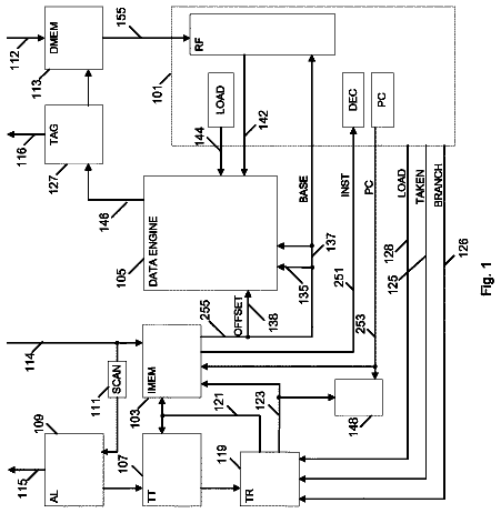
Sheet 1 of 18 from the published document. All sheets in the USPTO PDF
An apparatus and method are described for performing efficient gather operations in a pipelined processor. For example, a processor according to one embodiment of the invention comprises: gather setup logic to execute one or more gather setup operations in anticipation of one or more gather operations, the gather setup operations to determine one or more addresses of vector data elements to be gathered by the gather operations; and gather logic to execute the one or more gather operations to gather the vector data elements using the one or more addresses determined by the gather setup operations.
Field of the Invention This invention relates generally to the field of computer processors. More particularly, the invention relates to an apparatus and method for performing efficient gather and scatter operations. Description of the Related Art “Gather” and “scatter” operations are used to work with large, sparsely populated matrices. For example, existing computer processors perform gather operations to collect the elements of a matrix from memory and store them in a highly compressed format (e.g., sorted contiguously in an ordered array). Conversely, to perform various matrix operations (e.g., matrix multiplication) existing computer processors execute scatter operations to reproduce the previously-gathered matrix in memory.
1 of 18 drawing sheets so far from the published document, cropped to the drawing. Every sheet is in the USPTO PDF.
What the patent claimed, word for word. All of it is now free to use.
Field of the Invention
This invention relates generally to the field of computer processors. More particularly, the invention relates to an apparatus and method for performing efficient gather and scatter operations.
Description of the Related Art
“Gather” and “scatter” operations are used to work with large, sparsely populated matrices. For example, existing computer processors perform gather operations to collect the elements of a matrix from memory and store them in a highly compressed format (e.g., sorted contiguously in an ordered array). Conversely, to perform various matrix operations (e.g., matrix multiplication) existing computer processors execute scatter operations to reproduce the previously-gathered matrix in memory.
A better understanding of the present invention can be obtained from the following detailed description in conjunction with the following drawings, in which:
FIG. 1A is a block diagram illustrating both an exemplary in-order pipeline and an exemplary register renaming, out-of-order issue/execution pipeline according to embodiments of the invention;
FIG. 1B is a block diagram illustrating both an exemplary embodiment of an in-order architecture core and an exemplary register renaming, out-of-order issue/execution architecture core to be included in a processor according to embodiments of the invention;
FIG. 2 is a block diagram of a single core processor and a multicore processor with integrated memory controller and graphics according to embodiments of the invention;
FIG. 3 illustrates a block diagram of a system in accordance with one embodiment of the present invention;
FIG. 4 illustrates a block diagram of a second system in accordance with an embodiment of the present invention;
FIG. 5 illustrates a block diagram of a third system in accordance with an embodiment of the present invention;
FIG. 6 illustrates a block diagram of a system on a chip (SoC) in accordance with an embodiment of the present invention;
FIG. 7 illustrates a block diagram contrasting the use of a software instruction converter to convert binary instructions in a source instruction set to binary instructions in a target instruction set according to embodiments of the invention;
FIG. 8 illustrates a processor architecture in which embodiments of the invention may be implemented.
FIGS. 9A-C illustrate efficient gather/scatter operations in accordance with one embodiment of the invention.
FIGS. 10A-B illustrate methods for performing efficient gather/scatter operations in accordance with one embodiment of the invention.
FIGS. 11A and 11B are block diagrams illustrating a generic vector friendly instruction format and instruction templates thereof according to embodiments of the invention;
FIGS. 12A-D are block diagrams illustrating an exemplary specific vector friendly instruction format according to embodiments of the invention; and
FIG. 13 is a block diagram of a register architecture according to one embodiment of the invention.
In the following description, for the purposes of explanation, numerous specific details are set forth in order to provide a thorough understanding of the embodiments of the invention described below. It will be apparent, however, to one skilled in the art that the embodiments of the invention may be practiced without some of these specific details. In other instances, well-known structures and devices are shown in block diagram form to avoid obscuring the underlying principles of the embodiments of the invention. Exemplary Processor Architectures and Data Types
FIG. 1A is a block diagram illustrating both an exemplary in-order pipeline and an exemplary register renaming, out-of-order issue/execution pipeline according to embodiments of the invention. FIG. 1B is a block diagram illustrating both an exemplary embodiment of an in-order architecture core and an exemplary register renaming, out-of-order issue/execution architecture core to be included in a processor according to embodiments of the invention. The solid lined boxes in FIGS. 1A-B illustrate the in-order pipeline and in-order core, while the optional addition of the dashed lined boxes illustrates the register renaming, out-of-order issue/execution pipeline and core. Given that the in-order aspect is a subset of the out-of-order aspect, the out-of-order aspect will be described.
In FIG. 1A , a processor pipeline 100 includes a fetch stage 102 , a length decode stage 104 , a decode stage 106 , an allocation stage 108 , a renaming stage 110 , a scheduling (also known as a dispatch or issue) stage 112 , a register read/memory read stage 114 , an execute stage 116 , a write back/memory write stage 118 , an exception handling stage 122 , and a commit stage 124 .
FIG. 1B shows processor core 190 including a front end unit 130 coupled to an execution engine unit 150 , and both are coupled to a memory unit 170 . The core 190 may be a reduced instruction set computing (RISC) core, a complex instruction set computing (CISC) core, a very long instruction word (VLIW) core, or a hybrid or alternative core type. As yet another option, the core 190 may be a special-purpose core, such as, for example, a network or communication core, compression engine, coprocessor core, general purpose computing graphics processing unit (GPGPU) core, graphics core, or the like.
The front end unit 130 includes a branch prediction unit 132 coupled to an instruction cache unit 134 , which is coupled to an instruction translation lookaside buffer (TLB) 136 , which is coupled to an instruction fetch unit 138 , which is coupled to a decode unit 140 . The decode unit 140 (or decoder) may decode instructions, and generate as an output one or more micro-operations, microcode entry points, microinstructions, other instructions, or other control signals, which are decoded from, or which otherwise reflect, or are derived from, the original instructions. The decode unit 140 may be implemented using various different mechanisms. Examples of suitable mechanisms include, but are not limited to, look-up tables, hardware implementations, programmable logic arrays (PLAs), microcode read only memories (ROMs), etc. In one embodiment, the core 190 includes a microcode ROM or other medium that stores microcode for certain macroinstructions (e.g., in decode unit 140 or otherwise within the front end unit 130 ). The decode unit 140 is coupled to a rename/allocator unit 152 in the execution engine unit 150 .
The execution engine unit 150 includes the rename/allocator unit 152 coupled to a retirement unit 154 and a set of one or more scheduler unit(s) 156 . The scheduler unit(s) 156 represents any number of different schedulers, including reservations stations, central instruction window, etc. The scheduler unit(s) 156 is coupled to the physical register file(s) unit(s) 158 . Each of the physical register file(s) units 158 represents one or more physical register files, different ones of which store one or more different data types, such as scalar integer, scalar floating point, packed integer, packed floating point, vector integer, vector floating point, status (e.g., an instruction pointer that is the address of the next instruction to be executed), etc. In one embodiment, the physical register file(s) unit 158 comprises a vector registers unit, a write mask registers unit, and a scalar registers unit. These register units may provide architectural vector registers, vector mask registers, and general purpose registers. The physical register file(s) unit(s) 158 is overlapped by the retirement unit 154 to illustrate various ways in which register renaming and out-of-order execution may be implemented (e.g., using a reorder buffer(s) and a retirement register file(s); using a future file(s), a history buffer(s), and a retirement register file(s); using a register maps and a pool of registers; etc.). The retirement unit 154 and the physical register file(s) unit(s) 158 are coupled to the execution cluster(s) 160 . The execution cluster(s) 160 includes a set of one or more execution units 162 and a set of one or more memory access units 164 . The execution units 162 may perform various operations (e.g., shifts, addition, subtraction, multiplication) and on various types of data (e.g., scalar floating point, packed integer, packed floating point, vector integer, vector floating point). While some embodiments may include a number of execution units dedicated to specific functions or sets of functions, other embodiments may include only one execution unit or multiple execution units that all perform all functions. The scheduler unit(s) 156 , physical register file(s) unit(s) 158 , and execution cluster(s) 160 are shown as being possibly plural because certain embodiments create separate pipelines for certain types of data/operations (e.g., a scalar integer pipeline, a scalar floating point/packed integer/packed floating point/vector integer/vector floating point pipeline, and/or a memory access pipeline that each have their own scheduler unit, physical register file(s) unit, and/or execution cluster—and in the case of a separate memory access pipeline, certain embodiments are implemented in which only the execution cluster of this pipeline has the memory access unit(s) 164 ). It should also be understood that where separate pipelines are used, one or more of these pipelines may be out-of-order issue/execution and the rest in-order.
The set of memory access units 164 is coupled to the memory unit 170 , which includes a data TLB unit 172 coupled to a data cache unit 174 coupled to a level 2 (L2) cache unit 176 . In one exemplary embodiment, the memory access units 164 may include a load unit, a store address unit, and a store data unit, each of which is coupled to the data TLB unit 172 in the memory unit 170 . The instruction cache unit 134 is further coupled to a level 2 (L2) cache unit 176 in the memory unit 170 . The L2 cache unit 176 is coupled to one or more other levels of cache and eventually to a main memory.
By way of example, the exemplary register renaming, out-of-order issue/execution core architecture may implement the pipeline 100 as follows: 1) the instruction fetch 138 performs the fetch and length decoding stages 102 and 104 ; 2) the decode unit 140 performs the decode stage 106 ; 3) the rename/allocator unit 152 performs the allocation stage 108 and renaming stage 110 ; 4) the scheduler unit(s) 156 performs the schedule stage 112 ; 5) the physical register file(s) unit(s) 158 and the memory unit 170 perform the register read/memory read stage 114 ; the execution cluster 160 perform the execute stage 116 ; 6) the memory unit 170 and the physical register file(s) unit(s) 158 perform the write back/memory write stage 118 ; 7) various units may be involved in the exception handling stage 122 ; and 8) the retirement unit 154 and the physical register file(s) unit(s) 158 perform the commit stage 124 .
The core 190 may support one or more instructions sets (e.g., the x86 instruction set (with some extensions that have been added with newer versions); the MIPS instruction set of MIPS Technologies of Sunnyvale, Calif.; the ARM instruction set (with optional additional extensions such as NEON) of ARM Holdings of Sunnyvale, Calif.), including the instruction(s) described herein. In one embodiment, the core 190 includes logic to support a packed data instruction set extension (e.g., AVX 1 , AVX 2 , and/or some form of the generic vector friendly instruction format (U=0 and/or U=1), described below), thereby allowing the operations used by many multimedia applications to be performed using packed data.
It should be understood that the core may support multithreading (executing two or more parallel sets of operations or threads), and may do so in a variety of ways including time sliced multithreading, simultaneous multithreading (where a single physical core provides a logical core for each of the threads that physical core is simultaneously multithreading), or a combination thereof (e.g., time sliced fetching and decoding and simultaneous multithreading thereafter such as in the Intel® Hyperthreading technology).
While register renaming is described in the context of out-of-order execution, it should be understood that register renaming may be used in an in-order architecture. While the illustrated embodiment of the processor also includes separate instruction and data cache units 134 / 174 and a shared L2 cache unit 176 , alternative embodiments may have a single internal cache for both instructions and data, such as, for example, a Level 1 (L1) internal cache, or multiple levels of internal cache. In some embodiments, the system may include a combination of an internal cache and an external cache that is external to the core and/or the processor. Alternatively, all of the cache may be external to the core and/or the processor.
FIG. 2 is a block diagram of a processor 200 that may have more than one core, may have an integrated memory controller, and may have integrated graphics according to embodiments of the invention. The solid lined boxes in FIG. 2 illustrate a processor 200 with a single core 202 A, a system agent 210 , a set of one or more bus controller units 216 , while the optional addition of the dashed lined boxes illustrates an alternative processor 200 with multiple cores 202 A-N, a set of one or more integrated memory controller unit(s) 214 in the system agent unit 210 , and special purpose logic 208 .
Thus, different implementations of the processor 200 may include: 1) a CPU with the special purpose logic 208 being integrated graphics and/or scientific (throughput) logic (which may include one or more cores), and the cores 202 A-N being one or more general purpose cores (e.g., general purpose in-order cores, general purpose out-of-order cores, a combination of the two); 2) a coprocessor with the cores 202 A-N being a large number of special purpose cores intended primarily for graphics and/or scientific (throughput); and 3) a coprocessor with the cores 202 A-N being a large number of general purpose in-order cores. Thus, the processor 200 may be a general-purpose processor, coprocessor or special-purpose processor, such as, for example, a network or communication processor, compression engine, graphics processor, GPGPU (general purpose graphics processing unit), a high-throughput many integrated core (MIC) coprocessor (including 30 or more cores), embedded processor, or the like. The processor may be implemented on one or more chips. The processor 200 may be a part of and/or may be implemented on one or more substrates using any of a number of process technologies, such as, for example, BiCMOS, CMOS, or NMOS.
The memory hierarchy includes one or more levels of cache within the cores, a set or one or more shared cache units 206 , and external memory (not shown) coupled to the set of integrated memory controller units 214 . The set of shared cache units 206 may include one or more mid-level caches, such as level 2 (L2), level 3 (L3), level 4 (L4), or other levels of cache, a last level cache (LLC), and/or combinations thereof. While in one embodiment a ring based interconnect unit 212 interconnects the integrated graphics logic 208 , the set of shared cache units 206 , and the system agent unit 210 /integrated memory controller unit(s) 214 , alternative embodiments may use any number of well-known techniques for interconnecting such units. In one embodiment, coherency is maintained between one or more cache units 206 and cores 202 -A-N.
In some embodiments, one or more of the cores 202 A-N are capable of multi-threading. The system agent 210 includes those components coordinating and operating cores 202 A-N. The system agent unit 210 may include for example a power control unit (PCU) and a display unit. The PCU may be or include logic and components needed for regulating the power state of the cores 202 A-N and the integrated graphics logic 208 . The display unit is for driving one or more externally connected displays.
The cores 202 A-N may be homogenous or heterogeneous in terms of architecture instruction set; that is, two or more of the cores 202 A-N may be capable of execution the same instruction set, while others may be capable of executing only a subset of that instruction set or a different instruction set.
FIGS. 3-6 are block diagrams of exemplary computer architectures. Other system designs and configurations known in the arts for laptops, desktops, handheld PCs, personal digital assistants, engineering workstations, servers, network devices, network hubs, switches, embedded processors, digital signal processors (DSPs), graphics devices, video game devices, set-top boxes, micro controllers, cell phones, portable media players, hand held devices, and various other electronic devices, are also suitable. In general, a huge variety of systems or electronic devices capable of incorporating a processor and/or other execution logic as disclosed herein are generally suitable.
Referring now to FIG. 3 , shown is a block diagram of a system 300 in accordance with one embodiment of the present invention. The system 300 may include one or more processors 310 , 315 , which are coupled to a controller hub 320 . In one embodiment the controller hub 320 includes a graphics memory controller hub (GMCH) 390 and an Input/Output Hub (IOH) 350 (which may be on separate chips); the GMCH 390 includes memory and graphics controllers to which are coupled memory 340 and a coprocessor 345 ; the IOH 350 is couples input/output (I/O) devices 360 to the GMCH 390 . Alternatively, one or both of the memory and graphics controllers are integrated within the processor (as described herein), the memory 340 and the coprocessor 345 are coupled directly to the processor 310 , and the controller hub 320 in a single chip with the IOH 350 .
The optional nature of additional processors 315 is denoted in FIG. 3 with broken lines. Each processor 310 , 315 may include one or more of the processing cores described herein and may be some version of the processor 200 .
The memory 340 may be, for example, dynamic random access memory (DRAM), phase change memory (PCM), or a combination of the two. For at least one embodiment, the controller hub 320 communicates with the processor(s) 310 , 315 via a multi-drop bus, such as a frontside bus (FSB), point-to-point interface such as QuickPath Interconnect (QPI), or similar connection 395 .
In one embodiment, the coprocessor 345 is a special-purpose processor, such as, for example, a high-throughput MIC processor, a network or communication processor, compression engine, graphics processor, GPGPU, embedded processor, or the like. In one embodiment, controller hub 320 may include an integrated graphics accelerator.
There can be a variety of differences between the physical resources 310 , 315 in terms of a spectrum of metrics of merit including architectural, microarchitectural, thermal, power consumption characteristics, and the like.
In one embodiment, the processor 310 executes instructions that control data processing operations of a general type. Embedded within the instructions may be coprocessor instructions. The processor 310 recognizes these coprocessor instructions as being of a type that should be executed by the attached coprocessor 345 . Accordingly, the processor 310 issues these coprocessor instructions (or control signals representing coprocessor instructions) on a coprocessor bus or other interconnect, to coprocessor 345 . Coprocessor(s) 345 accept and execute the received coprocessor instructions.
Referring now to FIG. 4 , shown is a block diagram of a first more specific exemplary system 400 in accordance with an embodiment of the present invention. As shown in FIG. 4 , multiprocessor system 400 is a point-to-point interconnect system, and includes a first processor 470 and a second processor 480 coupled via a point-to-point interconnect 450 . Each of processors 470 and 480 may be some version of the processor 200 . In one embodiment of the invention, processors 470 and 480 are respectively processors 310 and 315 , while coprocessor 438 is coprocessor 345 . In another embodiment, processors 470 and 480 are respectively processor 310 coprocessor 345 .
Processors 470 and 480 are shown including integrated memory controller (IMC) units 472 and 482 , respectively. Processor 470 also includes as part of its bus controller units point-to-point (P-P) interfaces 476 and 478 ; similarly, second processor 480 includes P-P interfaces 486 and 488 . Processors 470 , 480 may exchange information via a point-to-point (P-P) interface 450 using P-P interface circuits 478 , 488 . As shown in FIG. 4 , IMCs 472 and 482 couple the processors to respective memories, namely a memory 432 and a memory 434 , which may be portions of main memory locally attached to the respective processors.
Processors 470 , 480 may each exchange information with a chipset 490 via individual P-P interfaces 452 , 454 using point to point interface circuits 476 , 494 , 486 , 498 . Chipset 490 may optionally exchange information with the coprocessor 438 via a high-performance interface 439 . In one embodiment, the coprocessor 438 is a special-purpose processor, such as, for example, a high-throughput MIC processor, a network or communication processor, compression engine, graphics processor, GPGPU, embedded processor, or the like.
A shared cache (not shown) may be included in either processor or outside of both processors, yet connected with the processors via P-P interconnect, such that either or both processors' local cache information may be stored in the shared cache if a processor is placed into a low power mode.
Chipset 490 may be coupled to a first bus 416 via an interface 496 . In one embodiment, first bus 416 may be a Peripheral Component Interconnect (PCI) bus, or a bus such as a PCI Express bus or another third generation I/O interconnect bus, although the scope of the present invention is not so limited.
As shown in FIG. 4 , various I/O devices 414 may be coupled to first bus 416 , along with a bus bridge 418 which couples first bus 416 to a second bus 420 . In one embodiment, one or more additional processor(s) 415 , such as coprocessors, high-throughput MIC processors, GPGPU's, accelerators (such as, e.g., graphics accelerators or digital signal processing (DSP) units), field programmable gate arrays, or any other processor, are coupled to first bus 416 . In one embodiment, second bus 420 may be a low pin count (LPC) bus. Various devices may be coupled to a second bus 420 including, for example, a keyboard and/or mouse 422 , communication devices 427 and a storage unit 428 such as a disk drive or other mass storage device which may include instructions/code and data 430 , in one embodiment. Further, an audio I/O 424 may be coupled to the second bus 420 . Note that other architectures are possible. For example, instead of the point-to-point architecture of FIG. 4 , a system may implement a multi-drop bus or other such architecture.
Referring now to FIG. 5 , shown is a block diagram of a second more specific exemplary system 500 in accordance with an embodiment of the present invention. Like elements in FIGS. 4 and 5 bear like reference numerals, and certain aspects of FIG. 4 have been omitted from FIG. 5 in order to avoid obscuring other aspects of FIG. 5 .
FIG. 5 illustrates that the processors 470 , 480 may include integrated memory and I/O control logic (“CL”) 472 and 482 , respectively. Thus, the CL 472 , 482 include integrated memory controller units and include I/O control logic. FIG. 5 illustrates that not only are the memories 432 , 434 coupled to the CL 472 , 482 , but also that I/O devices 514 are also coupled to the control logic 472 , 482 . Legacy I/O devices 515 are coupled to the chipset 490 .
Referring now to FIG. 6 , shown is a block diagram of a SoC 600 in accordance with an embodiment of the present invention. Similar elements in FIG. 2 bear like reference numerals. Also, dashed lined boxes are optional features on more advanced SoCs. In FIG. 6 , an interconnect unit(s) 602 is coupled to: an application processor 610 which includes a set of one or more cores 202 A-N and shared cache unit(s) 206 ; a system agent unit 210 ; a bus controller unit(s) 216 ; an integrated memory controller unit(s) 214 ; a set or one or more coprocessors 620 which may include integrated graphics logic, an image processor, an audio processor, and a video processor; an static random access memory (SRAM) unit 630 ; a direct memory access (DMA) unit 632 ; and a display unit 640 for coupling to one or more external displays. In one embodiment, the coprocessor(s) 620 include a special-purpose processor, such as, for example, a network or communication processor, compression engine, GPGPU, a high-throughput MIC processor, embedded processor, or the like.
Embodiments of the mechanisms disclosed herein may be implemented in hardware, software, firmware, or a combination of such implementation approaches. Embodiments of the invention may be implemented as computer programs or program code executing on programmable systems comprising at least one processor, a storage system (including volatile and non-volatile memory and/or storage elements), at least one input device, and at least one output device.
Program code, such as code 430 illustrated in FIG. 4 , may be applied to input instructions to perform the functions described herein and generate output information. The output information may be applied to one or more output devices, in known fashion. For purposes of this application, a processing system includes any system that has a processor, such as, for example; a digital signal processor (DSP), a microcontroller, an application specific integrated circuit (ASIC), or a microprocessor.
The program code may be implemented in a high level procedural or object oriented programming language to communicate with a processing system. The program code may also be implemented in assembly or machine language, if desired. In fact, the mechanisms described herein are not limited in scope to any particular programming language. In any case, the language may be a compiled or interpreted language.
One or more aspects of at least one embodiment may be implemented by representative instructions stored on a machine-readable medium which represents various logic within the processor, which when read by a machine causes the machine to fabricate logic to perform the techniques described herein. Such representations, known as “IP cores” may be stored on a tangible, machine readable medium and supplied to various customers or manufacturing facilities to load into the fabrication machines that actually make the logic or processor.
Such machine-readable storage media may include, without limitation, non-transitory, tangible arrangements of articles manufactured or formed by a machine or device, including storage media such as hard disks, any other type of disk including floppy disks, optical disks, compact disk read-only memories (CD-ROMs), compact disk rewritable's (CD-RWs), and magneto-optical disks, semiconductor devices such as read-only memories (ROMs), random access memories (RAMs) such as dynamic random access memories (DRAMs), static random access memories (SRAMs), erasable programmable read-only memories (EPROMs), flash memories, electrically erasable programmable read-only memories (EEPROMs), phase change memory (PCM), magnetic or optical cards, or any other type of media suitable for storing electronic instructions.
Accordingly, embodiments of the invention also include non-transitory, tangible machine-readable media containing instructions or containing design data, such as Hardware Description Language (HDL), which defines structures, circuits, apparatuses, processors and/or system features described herein. Such embodiments may also be referred to as program products.
In some cases, an instruction converter may be used to convert an instruction from a source instruction set to a target instruction set. For example, the instruction converter may translate (e.g., using static binary translation, dynamic binary translation including dynamic compilation), morph, emulate, or otherwise convert an instruction to one or more other instructions to be processed by the core. The instruction converter may be implemented in software, hardware, firmware, or a combination thereof. The instruction converter may be on processor, off processor, or part on and part off processor.
FIG. 7 is a block diagram contrasting the use of a software instruction converter to convert binary instructions in a source instruction set to binary instructions in a target instruction set according to embodiments of the invention. In the illustrated embodiment, the instruction converter is a software instruction converter, although alternatively the instruction converter may be implemented in software, firmware, hardware, or various combinations thereof. FIG. 7 shows a program in a high level language 702 may be compiled using an x86 compiler 704 to generate x86 binary code 706 that may be natively executed by a processor with at least one x86 instruction set core 716 . The processor with at least one x86 instruction set core 716 represents any processor that can perform substantially the same functions as an Intel processor with at least one x86 instruction set core by compatibly executing or otherwise processing
a substantial portion of the instruction set of the Intel x86 instruction set core or
object code versions of applications or other software targeted to run on an Intel processor with at least one x86 instruction set core, in order to achieve substantially the same result as an Intel processor with at least one x86 instruction set core. The x86 compiler 704 represents a compiler that is operable to generate x86 binary code 706 (e.g., object code) that can, with or without additional linkage processing, be executed on the processor with at least one x86 instruction set core 716 . Similarly, FIG. 7 shows the program in the high level language 702 may be compiled using an alternative instruction set compiler 708 to generate alternative instruction set binary code 710 that may be natively executed by a processor without at least one x86 instruction set core 714 (e.g., a processor with cores that execute the MIPS instruction set of MIPS Technologies of Sunnyvale, Calif. and/or that execute the ARM instruction set of ARM Holdings of Sunnyvale, Calif.). The instruction converter 712 is used to convert the x86 binary code 706 into code that may be natively executed by the processor without an x86 instruction set core 714 . This converted code is not likely to be the same as the alternative instruction set binary code 710 because an instruction converter capable of this is difficult to make; however, the converted code will accomplish the general operation and be made up of instructions from the alternative instruction set. Thus, the instruction converter 712 represents software, firmware, hardware, or a combination thereof that, through emulation, simulation or any other process, allows a processor or other electronic device that does not have an x86 instruction set processor or core to execute the x86 binary code 706 . System and Method for Efficient Gather and Scatter Operations
The embodiments of the invention described below provide techniques for performing gather and scatter operations in a high-performance manner. While some of the embodiments described below will focus on gather operations, it will be understood that the same principles may be applied to perform other operations such as scatter operations, gather to prefetch lines in the cache, and scatter to prefetch lines (in the exclusive state) in the cache.
In one embodiment, a gather operation takes as inputs: 1) A 64-bit base address in a general-purpose register; 2) A 512-bit index containing 16 element indices in a vector register; 3) A 16-bit mask indicating which elements are to be gathered.
The gather operation outputs its results to a 512-bit vector register and resets the mask bits corresponding to the successfully gathered elements.
This functionality is illustrated generally in FIG. 8 , which shows a 512-bit index register 800 storing 16 32-bit element indices which are added to a base address stored in GPR 802 for computing gather addresses. A 16-bit mask register 801 stores a bit value which is associated with each data element/address. If the mask register 801 stores a bit value of ‘1’ for a data element, then the gather logic 841 gathers the associated data element and stores the results in a destination vector register 803 . If the mask register 801 stores a bit value of ‘0’ for a data element, then the gather logic 841 does not gather the associated data element and store the result in the destination vector register 803 . As illustrated, in one embodiment, the destination vector register 803 is a 512-bit vector register for storing 16 32-bit packed/vector data elements (identified as “Elem 1 - 16 ”).
In one embodiment of the invention, the gather logic 841 includes gather setup logic 842 for performing a set-up phase to enable more efficient gather operations followed by a gather loop. In one embodiment, during the set-up phase, the gather setup logic 842 scans the mask 801 to identify the first element to be gathered, extracts an index from the 16 element indices 800 corresponding to the mask bit from mask register 801 , and performs an address computation by adding together the base register 802 , index from index register 800 , and optional displacement as described herein. The gather setup logic 842 may perform multiple setup instruction/operations to calculate multiple data element addresses prior to the execution of the first gather instruction/operation. As discussed below, in one embodiment, the gather setup logic 842 executes two gather setup instructions/operations prior to the execution of the first gather instruction/operation (see, e.g., FIG. 9B ).
In the gather loop, the gather logic 841 resets the mask bit corresponding to the last gathered element, finds the next set mask bit (e.g., the next bit set to ‘1’), extracts the corresponding index from index register 800 , computes the data element address, and loads the data element from memory into the destination vector register 803 . The gather loop is repeated until all vector data elements have been gathered. If a page fault or other exception occurs, the mask register 801 contains a bit vector of data elements that have not been gathered successfully.
As illustrated in FIG. 9A , an exemplary processor 955 on which embodiments of the invention may be implemented includes an execution unit 940 with gather logic 841 to execute gather set-up instructions and gather instructions as described herein. A register set 905 is provided with registers for storing the base address, mask bits, index data elements, and gathered data elements as shown in FIG. 8 as the execution unit 940 executes the gather set-up and gather instructions. Thus, the register set may include both general purpose registers (e.g., for storing the base address) and vector registers (for storing packed/vector data element addresses and packed/vector data elements).
The details of a single processor core (“Core 0 ”) are illustrated in FIG. 9A for simplicity. It will be understood, however, that each core shown in FIG. 9A may have the same set of logic as Core 0 . As illustrated, each core may also include a dedicated Level 1(L1) cache 912 and Level 2 (L2) cache 911 for caching instructions and data according to a specified cache management policy. The L1 cache 912 includes a separate instruction cache 920 for storing instructions and a separate data cache 921 for storing data. The instructions and data stored within the various processor caches are managed at the granularity of cache lines which may be a fixed size (e.g. 64, 128, 512 Bytes in length). Each core of this exemplary embodiment has an instruction fetch unit 910 for fetching instructions from main memory 900 and/or a shared Level 3 (L3) cache 916 ; a decode unit 930 for decoding the instructions (e.g., decoding program instructions into micro-operatons or “uops”); an execution unit 940 for executing the instructions (e.g., the gather set-up instructions as described herein); and a writeback unit 950 for retiring the instructions and writing back the results.
The instruction fetch unit 910 includes various well known components including a next instruction pointer 903 for storing the address of the next instruction to be fetched from memory 900 (or one of the caches); an instruction translation look-aside buffer (ITLB) 904 for storing a map of recently used virtual-to-physical instruction addresses to improve the speed of address translation; a branch prediction unit 902 for speculatively predicting instruction branch addresses; and branch target buffers (BTBs) 901 for storing branch addresses and target addresses. Once fetched, instructions are then streamed to the remaining stages of the instruction pipeline including the decode unit 930 , the execution unit 940 , and the writeback unit 950 . The structure and function of each of these units is well understood by those of ordinary skill in the art and will not be described here in detail to avoid obscuring the pertinent aspects of the different embodiments of the invention.
As mentioned above, the gather logic 841 of one embodiment includes gather setup logic 842 to reduce the pipeline latency between the address generation and vector execution of the gather instructions. One embodiment of the invention includes a set-up instruction/operation, referred to herein as “vgatherpf 0 hintdps,” that performs the set-up phase of the gather operation. The set-up instruction “primes” the gather hardware so that a subsequent gather instruction can execute gather operations more efficiently. Once primed, the gather loop runs at full speed.
An exemplary gather sequence shown in pseudocode follows:
TABLE-US-00001 mov rax, _linaddr vector_load_data64_indices mov rbx, _linaddr vector_load_data64_base vmovaps v1, [rax] mov eax, 0xffff kmovd k1, rax ; set 16-bit mask to all ones ;Gather Set-up vgatherpf0hintdps v2 {k1}, [rbx+v1] ; first gather set-up vgatherpf0hintdps v2 {k1}, [rbx+v1] ; second gather set-up ;Gather loop loop1: vgatherdps v2 {k1}, [rbx+v1] ; gather loop vgatherdps v2 {k1}, [rbx+v1] ; gather two elements per iteration jknz k1,loop1
The two gather set-up instructions “vgatherpf 0 hintdps” shown above compute speculative state in the gather logic 841 that allows the subsequent gather instructions “vgatherdps” to execute without an initial delay. In one embodiment, the speculative state does not become part of the architectural state and may be discarded without affecting the correctness of the gather operations. While the exemplary embodiment shows two gather set-up instructions to speculatively compute the first two iterations of the gather loop, a different number of gather set-up instructions may be used depending on the implementation (e.g., based on the multithreading capabilities of the processor on which the embodiments of the invention are employed).
The description continues in the full USPTO document.
About 6,290 words. The USPTO PDF has it with every drawing.
Fees are due 3.5, 7.5 and 11.5 years after grant. This patent expired on October 10, 2025, so the fee marked "not paid" was the one that went unpaid.
APPARATUS AND METHOD FOR EFFICIENT GATHER AND SCATTER OPERATIONS
Filed Sep 2012 · published Apr 2014Apparatus and method for efficient gather and scatter operations
Filed Sep 2012 · granted Oct 2017Earlier publications, parents and continuations. None of them can still be enforced, or this patent would not be listed.
Prior art cited by the examiner or applicant. Useful when you check your own idea for novelty.
Everything on this page comes from the documents linked above.