Cross-reference to related applications
This application is based upon and claims the benefit of priority from prior Japanese Patent Application No. 2015-131917, filed Jun. 30, 2015, the entire contents of which are incorporated herein by reference.
Background of the invention
1. Field of invention
The present invention relates to an imaging apparatus provided with an image stabilization unit.
2. Description of the related art
In recent years, digital cameras and video cameras have come to use high-density-pixel imaging elements capable of capturing high-resolution images, and there is an increasing demand for improvement of the positioning accuracy of image stabilization units. Some of the existing cameras are provided with a pixel-shift super-high resolution photographing function. According to this function, a number of images are photographed while moving an imaging element with accuracy lower than that defined by the pixel pitch, and the resultant images are synthesized as an image having a resolution higher than that of the imaging element. The pixel-shift super-high resolution photographing function requires higher positioning accuracy than that of ordinary photography.
Jpn. Pat. Appln. KOKAI Publication No. 2009-47756 proposes improving the position detection accuracy by changing the amplification factor and offset of a position detection circuit connected to a Hall sensor. In other words, according to Jpn. Pat. Appln. KOKAI Publication No. 2009-47756, an analog signal output from the Hall sensor is amplified, before it is converted into a digital signal and supplied to the position detection circuit. As a result, the digital signal subjected to the AD conversion can represent a position with high resolution. Accordingly, the position detection accuracy is improved.
Brief summary of the invention
According to a first aspect of the invention, there is provided an imaging apparatus comprising: an image stabilizing unit including (i) a movable portion provided with an imaging element or a photographing lens, (ii) a motor which drives the movable portion relative to a fixed portion, and (iii) a position detector which detects a position of the movable portion; a position signal processing unit which converts an analog signal output from the position detector into position information which is based on a movement amount of the movable portion; and a position signal processing control unit which applies first settings or second settings to the position signal processing unit, wherein the first settings enable the analog signal output from the position detector to be detected as a position in a whole movable range of the movable portion, and the second settings enable the analog signal output to be detected as a position in divided ranges obtained by dividing the whole movable range of the movable portion, wherein the position signal processing control unit applies the second settings based on an output obtained when the position signal processing unit is applied with the first settings.
According to a second aspect of the invention, there is provided an imaging apparatus comprising: an image stabilizing unit including (i) a movable portion provided with an imaging element or a photographing lens, (ii) a motor which drives the movable portion relative to a fixed portion, and (iii) a position detector which detects a position of the movable portion; a first position signal processing unit which converts an analog signal output from the position detector into position information which is based on a movement amount by which the movable portion moves in a whole movable range of the movable portion; a second position signal processing unit which changes an analog signal output from the position detector into position information which is obtained with respect to divided ranges obtained by dividing the whole movable range of the movable portion and which is more accurate than the position information provided by the first position signal processing unit; a position signal processing control unit which applies the second position signal processing unit with settings that enable the analog signal output from the position detector to be detected as a position in each of the divided ranges obtained by dividing the whole movable range of the movable portion; and a position signal processing selecting unit which selects either the first position signal processing unit or the second position signal processing unit, wherein the position signal processing control unit determines settings applied by the second position signal processing unit based on information provided by the first position signal processing unit.
Advantages of the invention will be set forth in the description which follows, and in part will be obvious from the description, or may be learned by practice of the invention. The advantages of the invention may be realized and obtained by means of the instrumentalities and combinations particularly pointed out hereinafter.
Brief description of the several views of the drawings
The accompanying drawings, which are incorporated in and constitute a part of the specification, illustrate embodiments of the invention, and together with the general description given above and the detailed description of the embodiments given below, serve to explain the principles of the invention.
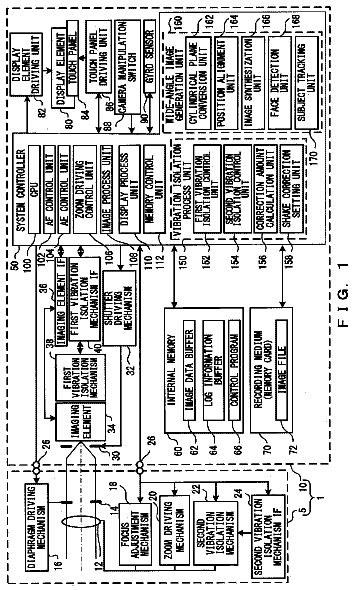
FIG. 1 schematically illustrates an imaging apparatus common to embodiments of the present invention.
FIG. 2 illustrates an assembled state of an image stabilization unit.
FIG. 3 is an exploded perspective view of the image stabilization unit.
FIG. 4 illustrates how a Hall sensor is arranged in a movable portion.
FIG. 5 is a functional block diagram illustrating an imaging apparatus according to the first embodiment.
FIG. 6 illustrates the circuit configuration of an example of a position detection circuit.
FIG. 7A shows an output which a position detection circuit produces in response to the stroke position of a movable portion when first settings are applied.
FIG. 7B shows an output which a position detection circuit produces in response to the stroke position of a movable portion when second settings are applied.
FIG. 8A shows a result obtained when that output of the position detection circuit shown in FIG. 7A is subjected to AD conversion.
FIG. 8B shows a result obtained when that output of the position detection circuit shown in FIG. 7B is subjected to AD conversion.
FIG. 9 shows an example of how constants A and B are determined.
FIG. 10A and FIG. 10B show examples of outputs from the position detection circuit.
FIG. 11A and FIG. 11B show examples of outputs from a position signal operation circuit.
FIG. 12A shows an example of a temperature characteristic of an output which the position detection circuit produces in response to the stroke position when first settings are applied.
FIG. 12B shows an example of a temperature characteristic of an output which the position detection circuit produces in response to the stroke position when second settings are applied.
FIG. 13 is a flowchart illustrating an operation of an image stabilization unit according to the first embodiment.
FIG. 14 is a flowchart illustrating a photographing operation according to the first embodiment.
FIG. 15 is a flowchart illustrating range switching processing according to the first embodiment.
FIG. 16 is a flowchart illustrating a super-high resolution photographing operation.
FIG. 17A and FIG. 17B shows examples of driving target positions in a super-high resolution photographing operation.
FIG. 18A and FIG. 18B illustrate how a range is divided when the position detection circuit has a nonlinear characteristic.
FIG. 19 is a functional block diagram illustrating an imaging apparatus according to the second embodiment.
FIG. 20 illustrates the circuit configurations of an example of a whole-range position detection circuit and an example of a high-accuracy position detection circuit.
FIG. 21 is a flowchart illustrating an operation of an image stabilization unit according to the second embodiment.
FIG. 22 is a flowchart illustrating a photographing operation according to the second embodiment.
FIG. 23 is a flowchart illustrating range switching processing according to the second embodiment.
Detailed description of the invention
Embodiments of the present invention will now be described with reference to the accompanying drawings. First Embodiment
The first embodiment will be explained below. FIG. 1 schematically illustrates an imaging apparatus common to embodiments of the present invention. The imaging apparatus 1 shown in FIG. 1 comprises an interchangeable lens 100 and a main body 200 . The interchangeable lens 100 is attached to the main body 200 by means of a mount 202 of the main body 200 . When attached to the main body 200 , the interchangeable lens 100 and the main body 200 connected in such a manner as to enable communications with each other. As a result, the interchangeable lens 100 and the main body 200 operate in cooperation with each other. The imaging apparatus 1 is not necessarily a lens interchangeable type. For example, the imaging apparatus 1 may be a lens-integral type imaging apparatus.
The interchangeable lens 100 comprises an optical system 102 . The optical system 102 includes, for example, a plurality of lenses and a diaphragm, and a light beam from an object (not shown) enters the image stabilization unit 206 of the main body 200 . Although the optical system 102 shown in FIG. 1 includes a plurality of lenses, it may include a single lens. The optical system 102 may include a focusing lens; alternatively, it may be configured as a zoom lens. In these cases, at least some of the lenses of the optical system 102 are movable in the Z direction, which is parallel to the optical axis O.
The main body 200 comprises a shutter 204 , an image stabilization unit 206 , a monitor 208 , an operation portion 210 and a control circuit 212 .
The shutter 204 is, for example, a focal plane shutter arranged on the front side of the image stabilization unit 206 (which side will be referred to as a positive side in the Z direction). When the shutter 204 is open, the image stabilization unit 206 is set in the exposed state. When the shutter 204 is closed, the image stabilization unit 206 is set in the light-shielded state.
When an image of an object, not shown, is taken, the image stabilization unit 206 generates a photograph image relating to the object. When the movable portion is moved relative to the fixed portions by means of a voice coil motor (VCM) made up of a coil and a magnet, the image stabilization unit 206 corrects the image blurring caused by hand shaking. The structure of the image stabilization unit 206 will be described in detail later.
The monitor 208 is, for example, a liquid crystal display and displays an image based on the photograph image generated by the image stabilization unit 206 . The monitor also displays a menu screen, which enables the user to enter various settings to the imaging apparatus 1 . The monitor 208 may be provided with a touch panel.
The operation portion 210 is, for example, a release button. The release button is a button with which the user instructs the start of the photographing operation by the imaging apparatus 1 . The operation portion 210 may include various operation elements other than the release button.
The control circuit 212 is made, for example, of an ASIC including a CPU and a memory, and controls the entire imaging apparatus 1 , including a photographing operation of the imaging apparatus 1 .
The structure of the image stabilization unit 206 will be described. FIG. 2 illustrates an assembled state of the image stabilization unit 206 . As shown in FIG. 2 , the image stabilization unit 206 includes two fixed portions 301 and 302 and a movable portion 303 sandwiched between the fixed portions 301 and 302 . With this structure, the image stabilization unit 206 permits the movable portion 303 to move in a plane perpendicular to the optical axis O (namely, in the X and Y directions shown in FIG. 2 ). In addition, the image stabilization unit 206 permits the movable portion 303 to rotate around the optical axis O.
First, a description will be given of the structure related to the movement of the movable portion 303 of the image stabilization unit 206 . FIG. 3 is an exploded perspective view of the image stabilization unit 206 . As shown in FIG. 3 , the fixed portion 301 located on the monitor ( 208 ) side of the movable portion 303 is a substantially rectangular plate member and is secured to the main body 200 . A magnet 3011 for movement in the X-direction and magnet 3012 for movement in both the X-direction and Y-direction are attached to the outer wall of the fixed portion 301 .
The magnet 3011 includes a rectangular first magnet. The first magnet has its longer sides extending in the Y direction and comprises an N pole facing the movable portion 303 . The magnet 3011 also includes a rectangular second magnet. The second magnet has its longer sides extending in the Y direction, but the longer sides of the second magnet are shorter than those of the first magnet. The second magnet comprises an S pole facing the movable portion 303 . The second magnet of the fixed portion 301 is arranged adjacent to the center portion of the right side of the first magnet, as viewed from the movable portion 303 . The magnet 3012 includes a rectangular first magnet. The first magnet has its longer sides extending in the Y direction and comprises an N pole facing the movable portion 303 . The magnet 3012 also includes a rectangular second magnet. The second magnet has its longer sides extending in the X direction, and the shorter sides of the second magnet extending in the Y direction are shorter than the longer sides of the first magnet. The second magnet comprises an S pole facing the movable portion 303 . The second magnet 301 is arranged adjacent to the center portion of the right side of the first magnet, as viewed from the movable portion 303 .
The magnet 3012 further includes a rectangular third magnet. The third magnet has its longer sides extending in the X direction, but the longer sides of the third magnet are shorter than those of the second magnet. The third magnet comprises an N pole facing the movable portion 303 . The third magnet 301 is arranged on the lower side of the second magnet, as viewed from the movable portion 303 . As can be seen, the second magnet of the magnet 3012 serves as a magnet for movement in the X direction in combination with the first magnet, and also serves as a magnet for movement in the Y direction in combination with the third magnet.
The fixed portion 302 located on the shutter ( 204 ) side of the movable portion 303 is a substantially L-shaped plate member comprising an opening in which an imaging element unit 3034 is held. A magnet 3021 for movement in the X-direction and magnet 3022 for movement in both the X-direction and Y-direction are attached to the fixed portion 301 at positions corresponding to the magnets 3011 and 3012 of the fixed portion. Magnet 3021 has a structure similar to that of magnet 3011 , and poles opposite to those of magnet 3011 face the movable portion 303 . Magnet 3022 has a structure similar to that of magnet 3012 , and poles opposite to those of magnet 3012 face the movable portion 303 .
The movable portion 303 is a substantially L-shaped plate member comprising an opening (similar to that of the fixed portion 302 ) in which an imaging element unit 3034 is held. Coils 3031 and 3032 a for movement in the X direction and coil 3032 b for movement in the Y direction are arranged on the outer wall of the movable portion 303 . Coil 3031 is provided on the plate portion extending in the Y direction and located at the position corresponding to magnets 3011 and 3021 . Coil 3032 a is provided on the plate portion extending in the Y direction and located at the position corresponding to the first and second magnets of magnets 3012 and 3022 . Coil 3032 b is provided on the plate portion extending in the X direction and located at the position corresponding to the second and third magnets of magnets 3012 and 3022 .
The imaging element unit 3034 is held in the opening of the movable portion 303 . The imaging element unit 3034 is a unit including an imaging element and a control circuit for controlling the imaging element. The imaging element unit 3034 of the present embodiment comprises an imaging element, a signal processor, an A/D conversion unit and an image processing unit. The imaging element captures an image of an object and generates a photographing image signal relating to the object. The signal processing unit performs analog processing for the photographing image signal, such as amplifying processing. The A/D converter converts the photographing image signal processed by the signal processing unit into a digital signal. The image processing unit performs image processing for the photographing image signal and generates a photographed image. In addition, the image processing unit synthesizes a number of photographed images and generates a super-high resolution image.
Fixed portion 301 is provided with two screw receivers 3015 , and fixed portion 302 is provided with screw-receiver holes 3025 at positions corresponding to the screw receivers 3015 . Fixed portion 302 is secured by means of screws in such a manner that the movable portion 303 is held between fixed portions 301 and 302 . It should be noted that coils 3031 , 3032 a and 3032 b are not in contact with magnets 3011 , 3012 , 3021 and 3022 ; there is a predetermined gap between the coils and the magnets.
With this structure, when a current supplied to one of the coils 3031 , 3032 a and 3032 b , the movable portion 303 is set in the floating state between the fixed portions 301 and 302 . The movable portion 303 is moved in parallel or rotated by controlling the driving currents supplied to the coils 3031 , 3032 a and 3032 b.
A description will now be given of a structure related to the position detection performed by the movable portion 303 . Three position detection magnets 3013 are provided on fixed portion 301 . One of the position detection magnets 3013 is located on the upper portion of fixed portion 301 . Another one of the position detection magnets 3013 is located on the lower portion of fixed portion 301 . The remaining one of the position detection magnets 3013 is located on the left portion of fixed portion 301 . As shown in FIG. 4 , three Hall sensors 3033 are provided on the reverse surface of the movable portion and located at positions corresponding to the position detection magnets. By a pair made up of the position detection magnet 3013 located in the upper portion of fixed portion 301 and the Hall sensor 3033 located in the upper portion of the movable portion 303 , a first displacement of the movable portion 303 in the X direction is detected as a change in the magnetic field. By a pair made up of the position detection magnet 3013 located in the lower portion of fixed portion 301 and the Hall sensor 3033 located in the lower portion of the movable portion 303 , a second displacement of the movable portion 303 in the X direction is detected as a change in the magnetic field. By a pair made up of the position detection magnet 3013 located in left portion of fixed portion 301 and the Hall sensor 3033 located in the left portion of the movable portion 303 , a displacement of the movable portion 303 in the Y direction is detected as a change in the magnetic field. The position of the movable portion 303 is detected based on the differences among the signals output from the Hall sensors 3033 .
FIG. 5 is a functional block diagram illustrating the imaging apparatus 1 according to the first embodiment. The imaging apparatus of the present embodiment performs image stabilization, an ordinary still image photographing operation and a super-high resolution photographing operation. The image stabilization is processing for moving the movable portion 303 in such a manner as to suppress the image blurring attributable to hand shaking or the like. The ordinary still image photographing operation is processing for performing a photographing operation once and generating one image thereby. The super-high resolution photographing operation is processing for performing a photographing operation a number of times while shifting the movable portion 303 by a distance less than the pixel pitch, synthesizing a number of images obtained thereby, and generating a photographed image having a resolution higher than that of an ordinary still image.
As shown in FIG. 5 , the imaging apparatus 1 comprises an image stabilization unit 206 , a position signal processing unit 402 , a position signal processing control unit 404 , a subtractor 406 , a driving control unit 408 and a motor driver 410 . These elements are expressed as functional blocks in FIG. 5 . These functions may be realized as hardware or as software. The position signal processing unit 402 , position signal processing control unit 404 , subtractor 406 , driving control unit 408 and motor driver 410 shown in FIG. 5 are provided such a manner that the number of each of these is equal to the number of VCMs. In the description of the present embodiment, only the structure corresponding to one VCM will be mentioned. In FIG. 5 , one of the VCMs provided in the image stabilization unit 206 (each VCM includes a magnet for movement and a coil) is shown as VCM 412 , and one of the Hall sensors 3033 provided in the image stabilization unit 206 is shown as Hall sensor 414 .
The position signal processing unit 402 receives an analog signal from the Hall sensor 414 of the image stabilization unit 206 , converts the received analog signal into a current position signal representing the position of the movable portion 303 , and supplies the current position signal to the subtractor 406 . The position signal processing unit 402 outputs the current position signal in accordance with either the first settings or the second settings. According to the first settings, an analog signal from the Hall sensor 414 is regarded as corresponding to the whole movable range of the movable portion 303 . According to the second settings, an analog signal from the Hall sensor 414 is regarded as corresponding to one of the divided movable ranges of the movable portion 303 .
The position signal processing unit 402 comprises a position detection circuit 4021 , an analog-to-digital converter (ADC) 4022 , a position signal calculation unit 4023 and a position signal correction unit 4024 .
The position detection circuit 4021 converts an analog signal output from the Hall sensor 414 into an analog signal corresponding to either the first settings or the second settings, and supplies the converted signal to the ADC 4022 . FIG. 6 illustrates the circuit configuration of an example of the position detection circuit 4021 . As shown in FIG. 6 , the position detection circuit 4021 shown as an example is a differential amplifier circuit for which an amplification factor and offset can be set. The differential amplifier 4021 includes an operational amplifier 4021 a , resistor 4021 b , resistor 4021 c , variable resistor 4021 d , variable resistor 4021 e , and digital-to-analog converter (DAC) 4021 f.
In FIG. 6 , the negative input terminal of the operational amplifier 4021 a is connected to one end of resistor 4021 b . The other end of resistor 4021 b is connected to one end of the Hall sensor 414 . The positive input terminal of the operational amplifier 4021 a is connected to one end of resistor 4021 c . The other end of resistor 4021 c is connected to the other end of the Hall sensor 414 . Variable resistor 4021 d is connected between one end of resistor 4021 b and the output terminal of the operational amplifier 4021 a . One end of variable resistor 4021 e is connected between the positive input terminal of the operational amplifier 4021 a and one end of resistor 4021 c . DAC 4021 f is connected to the other end of variable resistor 4021 e . With this structure, the amplification factor of the position detection circuit 4021 is determined in accordance with the resistance values of resistors 4021 b and 4021 a and the resistance values of variable resistors 4021 d and 4021 e . The offset of the position detection circuit 4021 is determined in accordance with the digital value of DAC 4021 f . The resistance values of variable resistors 4021 d and 4021 e and digital value of the offset entered to the DAC 4021 f are set by the position signal processing control unit 404 .
It should be noted that the configuration of the position detection circuit 4021 shown in FIG. 6 is merely an example. For example, in the position detection circuit 4021 shown in FIG. 6 , resistors 4021 b and 4021 c may be replaced with variable resistors and variable resistors 4021 d and 4021 e may be replaced with fixed resistors.
FIG. 7A shows an output which the position detection circuit 4021 produces in response to the stroke position (displacement) of the movable portion 303 when the first settings are applied. In the first settings, the amplification factor and the offset are determined in such a manner that the analog signal corresponding to the whole movable range of the movable portion 303 is in the range of the AD conversion of the ADC 4022 . For example, when the stroke position is maximal position A on the negative side of the movable range, the ADC 4022 outputs a voltage value corresponding to the lower limit of the AD conversion. When the stroke position of the movable portion 303 is maximal position D on the positive side of the movable range, the ADC 4022 outputs a voltage value corresponding to the upper limit of the AD conversion. Therefore, the amplification factor and offset can be individually determined in accordance with the sensitivity of the Hall sensor 414 .
FIG. 7B shows an output which the position detection circuit 4021 produces in response to the stroke position (displacement) of the movable portion 303 when the second settings are applied. According to the second settings, the movable range of the movable portion 303 is divided into a plurality of divided ranges in which the position detection resolution is equal (that is, the rate of change of the output of the position detection circuit 4021 to the change of the position of the movable portion 303 ). For example, where the output of the position detection circuit 4021 changes linearly in response to the change in the stroke position of the movable portion 303 , the movable range is divided equally. In the example shown in FIG. 7B , the movable range of the movable portion 303 is equally divided into three divided ranges, namely, range 1 , range 2 and range 3 . In the second settings, the amplification factor and the offset are determined such a manner that the analog signal is in the range of the AD conversion of the ADC 4022 in each of the divided ranges. For example, in range 1 , the amplification factor and offset are determined, such a manner that when the stroke position is maximal position A on the negative side of the movable range, the ADC 4022 outputs a voltage value corresponding to the lower limit of the AD conversion, and such a manner that when the stroke position of the movable portion 303 is maximal position B on the positive side of the movable range, the ADC 4022 outputs a voltage value corresponding to the upper limit of the AD conversion. In range 2 , the amplification factor and offset are determined, such a manner that when the stroke position is maximal position 3 on the negative side of the movable range, the ADC 4022 outputs a voltage value corresponding to the lower limit of the AD conversion, and such a manner that when the stroke position of the movable portion 303 is maximal position C on the positive side of the movable range, the ADC 4022 outputs a voltage value corresponding to the upper limit of the AD conversion. In range 3 , the amplification factor and offset are determined, such a manner that when the stroke position is maximal position C on the negative side of the movable range, the ADC 4022 outputs a voltage value corresponding to the lower limit of the AD conversion, and such a manner that when the stroke position of the movable portion 303 is maximal position D on the positive side of the movable range, the ADC 4022 outputs a voltage value corresponding to the upper limit of the AD conversion. Where the settings are determined in this manner, the straight line in range 1 , the straight line in range 2 and the straight line in range 3 have the same gradient. In other words, the position detection resolution is the same. The gradient of the straight line in each divided range is larger than the gradient of the straight line shown in FIG. 7A . According to the second settings, therefore, the amplification factor and offset can be individually determined in accordance with the sensitivity of the Hall sensor 414 . If the sensitivity of the Hall sensor 414 is high, the number of ranges may be larger than three.
The stroke position of the movable portion 303 can vary depending upon the temperature characteristic or the like. In practice, therefore, the amplification factor and offset should be preferably determined in consideration of the variations in the movable range. For example, in the first settings, the amplification factor and offset are determined, such a manner that when the stroke position of the movable portion 303 is position A′ less than position A by a predetermined distance, the ADC 4022 outputs a voltage value corresponding to the lower limit of the AD conversion, and such a manner that when the stroke position of the movable portion 303 is position D′ more than position D by a predetermined distance, the ADC 4022 outputs a voltage value corresponding to the upper limit of the AD conversion. In the second settings, the amplification factor and offset are determined for range 1 shown in FIG. 7B , such a manner that when the stroke position of the movable portion 303 is position A′ less than position A by a predetermined distance, the ADC 4022 outputs a voltage value corresponding to the lower limit of the AD conversion, and such a manner that when the stroke position of the movable portion 303 is position D′ more than position D by a predetermined distance, the ADC 4022 outputs a voltage value corresponding to the upper limit of the AD conversion. Likewise, the amplification factor and offset are determined for range 2 shown in FIG. 7B , such a manner that when the stroke position of the movable portion 303 is position B″ less than position B by a predetermined distance, the ADC 4022 outputs a voltage value corresponding to the lower limit of the AD conversion, and such a manner that when the stroke position of the movable portion 303 is position C′ more than position C by a predetermined distance, the ADC 4022 outputs a voltage value corresponding to the upper limit of the AD conversion. Likewise, the amplification factor and offset are determined for range 3 shown in FIG. 7B , such a manner that when the stroke position of the movable portion 303 is position C″ less than position C by a predetermined distance, the ADC 4022 outputs a voltage value corresponding to the lower limit of the AD conversion, and such a manner that when the stroke position of the movable portion 303 is position D′ more than position D by a predetermined distance, the ADC 4022 outputs a voltage value corresponding to the upper limit of the AD conversion.
Reference will be made back to FIG. 5 . The ADC 4022 converts an analog signal output from the position detection circuit 4021 into an AD value, which is a digital signal. FIG. 8A shows a result obtained when that output of the position detection circuit 4021 shown in FIG. 7A is subjected to AD conversion, and FIG. 8B shows a result obtained when that output (e.g., range 1 ) of the position detection circuit 4021 shown in FIG. 7B is subjected to AD conversion. As described above, the rate of change of the output of the position detection circuit 4021 to the change in the stroke position according to the second settings (that is, the gradient of the straight line shown in FIG. 7B ) is higher than the rate of change of the output of the position detection circuit 4021 to the change in the stroke position according to the first settings (that is, the gradient of the straight line shown in FIG. 7A ). Therefore, the resolution of the AD conversion according to the second settings (that is, the length [μm/LSB] represented by the least significant bit of the digital signal) is higher than the resolution of the AD conversion according to the first settings. That is, the second settings enable position detection to be performed with higher accuracy than the first settings.
The position signal calculation unit 4023 generates a current position signal, representing the current position of the movable portion 303 , from the AD value obtained by the ADC 4022 . The same position signal is generated without reference to the first settings and second settings. To be specific, whether the current settings are first settings or second settings, the current position signal representing the same position is generated for the analog signal output from the Hall sensor 414 . The current position signal is generated, for example, by the calculation defined in the following formula: Current Position= A ×( AD value)+ B
where the AD value is obtained by the ADC 4022 , and A and B are constants which are predetermined depending upon whether the current settings are first settings or second settings and in accordance with one of ranges 1 , 2 and 3 where the current settings are second settings.
FIG. 9 shows an example of how constants A and B are determined. The values of constants A and B shown in FIG. 9 are stored in a memory (not shown) of the position signal calculation unit 4023 . In the example shown in FIG. 9 , the ADC 402 is a 12-bit converter. The movable range of the movable portion 303 is −50 to 1050 μm. In consideration of the temperature characteristics of the movable portion 303 etc., the movable range is widened from the range of 1000 μm by ±50 μm. Of the movable range, range 1 is from −50 μm to 350 μm (400 μm), range 2 is from 300 μm to 700 μm (400 μm), and range 3 is from 650 μm to 1050 μm (400 μm). As mentioned above, in ranges 1 , 2 and 3 , the position detection resolution is equal. The resolution of the ADC 4022 is 0.29 [μm/LSB] according to first settings, and is 0.10 [μm/LDB] according to second settings. In these settings, constants A and B are determined in such a manner that the position detection resolution of a current position signal is 0.10 μm/LSB.
By determining constants A and B in the manner shown in FIG. 9 , the same current position signal can be generated in response to the stroke position of the movable portion 303 , without reference to where the movable portion 303 is located. For example, let us assume that in the first settings, the output of the position detection circuit 4021 corresponding to stroke position E in range 1 is V 1 [mV], as shown in FIG. 10A . Let us also assume that in the second settings, the output of the position detection circuit 4021 corresponding to stroke position E in range 1 is V 2 (V 1 <V 2 ) [mV], as shown in FIG. 10B . Where constants A and B are determined in the manner shown in FIG. 9 , the output of the position signal calculation unit 4023 is as shown in FIG. 11A according to the first settings, and is as shown in FIG. 11B according to the second settings. The straight line in FIG. 11B is the same as the straight line in FIG. 11A , except that it is a line in range 1 only. As can be seen from this, the output which the position signal calculation unit 4023 produces in response to the stroke position is the same whether the current settings are first settings or second settings.
The values of A and B in FIG. 9 are shown by way of example. The values of A and B may be varied in accordance with the width of the movable range of the movable portion 303 , the bit configuration of the ADC 4022 , the position detection resolution of the current position signal, etc.
The position signal correction unit 4024 corrects an error which may be included in the current position signal of the position signal calculation unit 4023 due to the temperature characteristic. The Hall sensor 414 has a temperature characteristic. Therefore, the position detection circuit 4021 may output different analog signals for the same position of the movable portion 303 . The current position signals generated based on such analog signals may represent different positions, depending upon temperature. The position signal correction unit 4024 corrects an error attributable to such a temperature characteristic.
FIG. 12A shows an example of a temperature characteristic of an output which the position detection circuit 4021 produces in response to the stroke position when the first settings are applied. In FIG. 12A , the broken line indicates an example of data obtained at normal temperature (at 20° C. or thereabouts), while the solid line indicates an example of data obtained at high temperature (at 40° C. or thereabouts). As described above, the Hall sensor 414 has a temperature characteristic. Therefore, the position detection circuit 4021 may output different analog signals with respect to the same stroke position. FIG. 12B shows an example of a temperature characteristic of an output which the position detection circuit 4021 produces in response to the stroke position when the second settings are applied. In FIG. 12B , the broken line indicates an example of data obtained at normal temperature (at 20° C. or thereabouts), while the solid line indicates an example of data obtained at high temperature (at 40° C. or thereabouts). As can be seen, the position detection circuit 4021 may output different analog signals with respect to the same stroke position, depending upon the temperature, not only when the first settings are applied but also when the second settings are applied. In order to correct the output differences which the position detection circuit 4021 may undergo due to the temperature characteristic, the position signal correction unit 4024 corrects the current position signal of the position signal calculation unit 4023 such a manner that it becomes identical to the current position signal obtained immediately after the switching between the first settings and the second settings. The correction value used for this purpose is a difference value between the current position signals obtained before and after the switching of settings.
The description continues in the full USPTO document.
 Lapsed, fee not paid8 drawings