Field of the invention
This invention relates generally to non-volatile memories and, more specifically, to using non-volatile memory of a NAND-type architecture perform on-chip data analytics.
Background of the invention
Content addressable memories, also known as associative memories, are different from standard memories in the way that data is addressed and retrieved. In a conventional memory, an address is supplied and the data located at this specified address is retrieved. In contrast, in a content addressable memory (CAM), data is written as a key-data pair. To retrieve the data, a search key is supplied and all the keys in the memory are searched for a match. If a match is found, the corresponding data is retrieved.
Content Addressable Memories, or CAMs, can be implemented in several ways. In one sort of embodiment, a CAM is implemented using a conventional memory and an associated CPU which searches through the memory to find a matching key. The keys in the memory may be sorted, in which case a binary search can be used; or they can be unsorted, in which case they are usually hashed into buckets and each bucket is searched linearly. A CAM can also be implemented as a semiconductor memory, where every memory location contains an n-bit comparator. When an n-bit key is provided, each entry in the CAM will compare the search key with the entry's key, and signal a match if the two are equal.
Summary of invention
A first set of aspects concern a method of performing data analytics using a server and a memory system connected to the server. The memory system includes control circuitry and a plurality of sets of memory arrays having a NAND type of architecture. The control circuitry including a plurality of memory controllers each associated with a corresponding set of memory arrays. The server runs software that issues commands to the memory system to perform one or more data analytic operations. The memory system receives the issued commands and translates them into a plurality of analytic tasks by firmware operating on the control circuitry. The firmware distributes the analytic tasks across the memory controllers to be executed by the memory controllers and corresponding sets memory of memory arrays. The analytic tasks are executed on the memory controllers and corresponding sets memory of memory arrays, wherein each of the analytic tasks are executed on the memory controller, the associated sets of memory arrays, or a combination of them as specified by the firmware. The final or medium results (final or inter mediate) from the analytic tasks are merged (by the server or firmware). The result can then be transferred out by the server as a graphical display. In this arrangement, the bottom memory layer can execute simple task on massive data. The middle layer of the flash controller or more sophisticated microprocessor can crunch more complicated data on lesser amounts of data. The combination of lower level data selection and upper level complicated computation can overcome the input/output limitations of the traditional data analytic system. Moving computing closer to the data also can save power as there is not the need to transfer all the data out.
Other aspects relate to methods of performing analytic operations on a plurality of sets of data. A memory system receives from a server a plurality of data sets and instructions for analytics to perform upon the data sets. The memory system includes control circuitry having one or more memory controllers and one or more memory circuits each having one or more memory arrays of non-volatile memory cells having a NAND type of architecture. The control circuitry breaks down the received instructions into a plurality of sub-operations and assigns one or more of the sub-operations to be performed on the control circuitry and one or more of the sub-operations to be performed within the memory circuits. The control circuitry derives from the received data sets a plurality of corresponding derived data sets for use in the sub-operations to be performed within the memory circuits and the derived data sets are written into one or more of the memory arrays, where the first derived data sets are written into the memory arrays oriented along bit lines. In some embodiments, duplicated data sets can be stored in the memory along word lines with normal ECC protection. The sub-operations can be operated on the data sets stored along the bit line direction for fast, but rough operations. Then operation results can be read out from the data set stored along the word line direction and more data analytics can be performed on the data sets. For any of the embodiments, the result of the analytics performed on the data sets are provided to the server.
Various aspects, advantages, features and embodiments of the present invention are included in the following description of exemplary examples thereof, which description should be taken in conjunction with the accompanying drawings. All patents, patent applications, articles, other publications, documents and things referenced herein are hereby incorporated herein by this reference in their entirety for all purposes. To the extent of any inconsistency or conflict in the definition or use of terms between any of the incorporated publications, documents or things and the present application, those of the present application shall prevail.
Brief description of the drawings
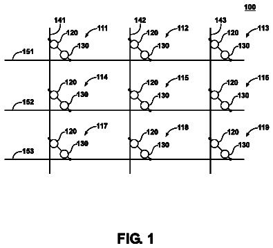
FIG. 1 is a schematic representation of a NAND array used as a CAM memory.
FIG. 2 is a schematic illustration of the network of some of the elements to supply the word line in a NAND array for conventional operation.
FIG. 3 is a schematic illustration of the network of some of the elements to supply the word line in a NAND array for CAM operation.
FIG. 4 shows one embodiment for how keys can be written along bit lines of an NAND array and searched.
FIG. 5 given some detail on how a key/inverse pair from FIG. 4 is programmed into a pair of NAND strings.
FIGS. 6A-C shows another embodiment for how keys can be written along bit lines of an NAND array and searched.
FIG. 7 shows an exemplary encoding of 2-bits per cells for four state memory cell operation.
FIG. 8 shows how the data states and the complementary data used for the inverted keys correspond in the 2-bit per cell example.
FIG. 9 shows an example of how a key would be encoded onto a 4 cell NAND string on bit line BL and its inverse on bit line BLB.
FIG. 10 illustrates the process of matching of content in word line direction.
FIG. 11 illustrates how the position of a conducting bit line can be used as an index in to another table that can be used to retrieve data associated with the target key.
FIG. 12 schematically illustrates how a key-value pair is stored in a NAND based CAM and how the value is accessed using the key.
FIG. 13 illustrates a memory arrangement for transposing the data keys.
FIG. 14 represents a first hardware embodiment for transposing data using a FIFO-type structure.
FIG. 15 represents another hardware embodiment for transposing data.
FIG. 16 shows one embodiment of a memory system incorporating a CAM type NAND into a solid state drive (SSD) for performing data analytic within the memory system.
FIG. 17 illustrates how data analytics with numerical range detection can be performed by exploiting an array's NAND structure.
FIG. 18 is an example of data latch assignments for the process illustrated by FIG. 17.
FIGS. 19 and 20 illustrate some steps of two search processes.
FIGS. 21 and 22 illustrate a maximum and a minimum search operation.
FIGS. 23 and 24 respectively give a schematic representation of an on-chip arithmetical operation and a corresponding latch utilization.
FIGS. 25A-C illustrate some detail of how arithmetic operations can be performed.
FIGS. 26A and 26B show how more latches can be used to perform arithmetic operations involving more n
FIGS. 27 and 28 illustrate an application to financial data analysis.
FIGS. 29-31 show some examples of how a data set can placed on more than on NAND string and corresponding latch structures.
FIGS. 32 and 33 respectively illustrate digital and analog counting techniques for analytics results.
FIG. 34 gives an example of file mapping for performing analytics on large file systems.
FIG. 35 illustrates a conventional architecture for server CPU based data analytics.
FIG. 36 illustrates an architecture using computational NAND in data analytics.
FIG. 37 shows a more detailed hardware architecture for a part of the data analytics system.
FIGS. 38A-D illustrate various aspects related performing to a "price summary report" query.
FIGS. 39A and 39B is a schematic representation of the division of tasks between the controller and NAND memory for the query of FIGS. 38A-D.
FIGS. 40A-D illustrate various aspects related performing to a "minimum cost supplier" query.
FIGS. 41A and 41B is a schematic representation of the division of tasks between the controller and NAND memory for the query of FIGS. 40A-D.
FIG. 42 illustrates the data structure using column and row storage.
FIG. 43 presents the relationship between the building blocks in the analytic system.
FIG. 44 is a schematic representation of a server based map reduce data analysis and how this can be moved to an CAM NAND based analytic system.
FIG. 45A illustrates a hardware architecture for a Hadoop arrangement and how CAM NAND can be incorporated.
FIG. 45B compares performance versus storage capacity for NAND based computing with CPU based computing.
FIG. 46 illustrates the use of CAM NAND memory based analytics for the sort and merge of un-structures data.
FIG. 47 schematically illustrates an example of when the sort is partially done in the SSD ASIC.
FIGS. 48-54 provides examples of analytic operations performed the CAM NAND based data analytics system.
Description of the preferred embodiments
Content Addressable Memory Based on NAND Flash Memory
The following presents a method of using a Flash based NAND memory array as a content addressable memory (CAM) that can be realized in both binary and ternary embodiments. As described in more detail below, keys can be programmed along the bit lines of a block. The search key is then input along the word lines of the blocks, so that a bit line on which a corresponding key has been programmed will be conducting. This allows for all the keys of a block to be checked at the same time.
The typical way by which a NAND memory array is read is that data is read out a single word line (or portion of a word line) at a time, with the non-selected word lines along the NAND strings being biased so that they are fully turned on regardless of the data state, removing the non-selected memory from affecting the read operation. In this way, the data content of the memory is read out a page (the unit of read) at a time. In contrast, to use a NAND flash memory as a content addressable memory, all of the word lines are set to a specific data dependent value, where the data is the key, and the memory determines which bit lines then conduct, thereby determining particular bit lines correspond to the input key, rather that the data of individual cells. An operation where sensing voltages are applied to multiple word lines in the context of an enhanced post-write read operation is given in U.S. patent application Ser. No. 13/332,780 filed on Dec. 21, 2011, (and which also presents more detail on NAND flash memory in general); however, even in that case only a few of the word lines receive a sensing voltage. Also, in prior art NAND memories, data was aligned along word lines, where data pages (for both read and write) are aligned along the word lines. Here, data is aligned along bit lines and many, or even all, of the word lines along the bit lines can receive either a high voltage sufficient to turn on a cell in a programmed state, or a low voltage sufficient to turn on a cell in the erased state. The following discussion will use the EEPROM based flash memory as the exemplary embodiment, but other memory devices having a NAND type of architecture, including 3D NAND (such as described in T. Maeda et al., "Multi-stacked 1 G cell/layer Pipe-shaped BiCS flash memory", 2009 Symposium on VLSI Circuits, pages 22-23) for example, can also be used.
In a binary, EEPROM based flash memory, in a write operation each cell is either left in an erased state or charge is placed on the cell's floating gate to put the cell in a programmed state, which here are respectively taken as the 1 and 0 states. When a low value for the read voltage is applied to its control gate, only a cell in the erased, or 1, state will conduct. For cells in the programmed, or 0, state, a high value of the read voltage needs to be applied to the control gate for a cell to conduct. The keys will be arranged along bit lines of a block of the memory array. Since a cell in the 1 state will conduct for either read voltage, each key needs to be written twice, in inverted and non-inverted form. As discussed below, this can be done by writing the target key along one bit line and its inverse along another, or writing half the bit line with the (non-inverted) target key and the other half of the bit line with the inverted target key. More key info can be compressed into the NAND chain using multiple bits programming. For example, in a 2-3 bits per cell case, the key can be sorted in the controller RAM and the bits will be programmed as lower, (middle) or upper pages. The following discussion will mostly be given in terms of a binary embodiment, with some specifics of the multi-state case are discussed later.
The general concept can be illustrated by FIG. 1. Target keys Key 0, Key 1, . . . are programmed down bit lines BL0, BL1, . . . of a NAND block. Data is programmed in a separate location that can be indexed by the target key's column address number. To search the block for a key, the search key is broadcasted on the block's word lines by setting all of the word lines according to either the high or low read voltage according to the search key. (In addition to setting the word line voltages according to the key, the select gates at the end of the NAND string will also need to be turned on.) Each BL effectively compares itself to the WL key pattern for all of the bit lines in the block at the same time. If the bit line key matches the search key, the whole of the bit line will be conducting and a "1" will be read out. (Note that, as discussed further, this discussion is somewhat simplified for the reasons discussed in the last paragraph.) Once the column index of the key is found, it can be used to fetch the corresponding data from a "data" block. The key can be the hash code of the data page that will lead to the right data page by the column address of the matched NAND chain. For content matching applications, such as data compression or de-duplication, each 16 KB, say, of content can generate a corresponding hash code that can be stored along the NAND chain. If the key along the NAND chain is matched, then the data page will be compared with the comparing data along the word line to avoid hash collision cases. In other cases, the content along the word line may not be a hash value, but characteristics of the data elements that can be searched as a keys to data; or the bits lines themselves main be the elements of the data themselves, rather than a pointer to a data base.
Under the arrangement illustrated by FIG. 1, all of the bit lines of the array, and consequently all of the keys, are searched at the same time. In arrays that do not use an all bit line type of architecture, the number of keys searched simultaneously would be the number of bit line sensed in parallel, such as half of the total in an odd-even arrangement. The size of the key is the number of word lines. In practice, these maximum values of the keys will typically be somewhat less, since some column are usually set aside for defects, for instance.
As noted above, since a memory cell in either the 0 or 1 state will conduct for a high read voltage, the key will need to be entered twice, both non-inverted and inverted. This can be done by either programming the target key on two bit lines, reducing the number of keys by half, or programming both versions of the key on the same bit line, reducing the key size by half. However, given the size of available NAND blocks, even with these reductions the number of keys that can be checked in parallel is quite large. Relative to some other memory technologies, NAND flash memory has relatively large latencies in its operation, but in many applications this would more than be offset by the number of keys (bit lines) that can be checked in parallel (128K, for example). The process can all be done on-chip and, as only the bit lines that meet the matching case conducting current, with relatively low power consumption, so that compared to toggling out all of the data from the memory and doing the compare in the controller, it is a process of relatively low power and higher speed.
Looking at some implementation detail, an exemplary embodiment can be based on a flash memory where the indices are saved on the 128 Gb NAND chains. An all bit line (ABL) architecture is used where one sensing operations will perform a match operation on all of the indices on a block at the same time. Extra column redundancy is included to avoid any bad columns (more detail on such redundancy and the accessing of columns, as well as flash memory in general, can be found in the following US patent publication/application numbers: US-2005-0141387-A1; US-2008-0266957-A1; US-2011-0002169-A1; US-2010-0329007-A1; Ser. No. 13/463,422; and Ser. No. 13/420,961.) Two copies of the same data, Data and Data Bar, are written into the NAND chain. In the example, this allows for 16 KB/2/2=32000 sets of information with a 128 bit key.
When writing in the keys, these will be typically written on a page by page basis, although in memories that allow it, partial page programming can be used to write part of the keys, with more added later. Such partial page programming is typically more limited for multi-states implementations than in binary blocks. As one example, the data can be shifted on to the memory and the inverted data can be generated on the memory to save effort on the controller for these data manipulations, where the data and data bar can be written without shifting in the data twice, with the data being written first, and the generated inverse next. Both the keys and the data can be input into the memory system, or in some cases the keys could be generated on the memory system by the controller from the data, such as by generating hash values from the data to use as keys. If the keys are to be sorted before being written along the bit lines, this will typically be done on the controller due to the amount of data involved, such as multiple blocks' worth of data. For example, the data could initially be written in a particular area, say die 0, plane 0, blocks 0-15, and then sorted and written into the blocks having been sorted to the block level. Alternately, the keys could be assembled in RAM (either on the controller or on a separate chip) or cache NAND memory (such as described in U.S. provisional application No. 61/713,038) before sorting them to the desired level of granularity and writing them into a set of blocks.
As discussed further below, the data/data bar pairs can be written on two bits lines or on a single bit line. When the data/data bar pairs are written on two bit lines, such as discussed with respect to FIG. 4, the pairs can be written next to each other or in other patterns, such as writing the data bit lines in one area and the inverted data bit lines in another zone. When both parts of the pair on written on the same bit line, as discussed below with respect to FIG. 6A, they can be written in a top/bottom format or interleaved. For example, when the data and inverted data are interleaved to alternates down the word lines, this has the advantage that at most two elements in a row are the same down the bit line; further, interleaving can lead to efficient data transfer on to the memory as first a page of data is transferred on the memory and the next page can just be generated in the latches by inverting all the bits, as the next page is the inverted data of the first page.
The matched index can then be linked to other data corresponding to the determined column address; for instance, the keys could be a hash value, such as from a Secure Hash Algorithm (SHA), used to point to the actual data that can also be stored elsewhere on the memory itself. All the matching can be done inside of the NAND chip and, when the match is found, the column address can also be transferred out if needed or just the data, if also stored on the NAND chip, can be transferred out.
To efficiently implement the use of a NAND array as a CAM memory, changes can be made to the word line driving circuitry. To broadcast a search key down the word lines of a block, in addition to turning on the select gates on either end of the NAND strings, each word line of the block needs to be set to either the high or low read voltage according to the search key. This is in contrast to typical NAND operation, where only a single word line at a time is selected for a read voltage, with all of the other word lines receiving a pass voltage sufficient to remove them from influencing the sensing regardless of their data state.
FIG. 2 is a schematic illustration of the network of some of the elements to supply the word line in a NAND array for conventional operation. At 201 is the cell array for a plane of a NAND chip, with two blocks explicitly marked out at 203 and 205. Each block's word lines are feed by a word line select gate WLSW 213 or 215 as controlled from select circuitry at 217. The bit lines are not indicated, but would run down to the sense amp block S/A 207. The various control gate voltage CGI are then supplied to the select gates 213 and 215 from the drivers CG drivers 231 and UCG drivers 233 and 235 by way of switches 223 and 225, respectively. In the exemplary embodiment shown here, a block is taken to have 132 word lines, where a pair of dummy word lines are included on both the drain and source sides of the NAND strings. The UCG Drivers 233 and 235 are for supplying the pass voltages used on unselected word lines during program, (standard, non-CAM) read or verify operations. As this level is used on the large majority of word lines, these can be lumped together for a single driver. The selected control gates are biased to VPGM at program, CGR voltage at read or verify. In FIG. 2, CGI<126:1> is the decoded global CG lines. CGI<0> and CGI<127>, that are here biased differently from other 126 word lines due to edge word line effects. The dummy word line bias CGD0/1 is for the drain side dummy word lines and CGDS0/1 is for the source side ones.
For a typical NAND memory operation, only a few word lines at a time are individually biased. In addition to a selected word line, adjacent or edge word lines may receive special bias levels to improve operations. Consequently, existing word line drivers are arranged so that they can only take care of a handful of word lines. With logic changes, it may be possible to drive up to perhaps two dozen or so word lines. However, to drive all the word lines of a block (here 128, ignoring dummies) will require additional analog drivers. FIG. 3 illustrates some of these changes.
The array 301, blocks 303 and 305, select circuitry 317, CG Drivers 331, and switches 313 and 315 can be the same as in FIG. 2. The additional word line drivers are shown at 343 and 345 and can supply the word lines through respective switches at 353 and 355. In each of 343 and 345, the level shifter HVLSHIFT receives the voltage VREAD and a digital value DFF(0/1) for each word line. The level shifter then converts the digital values of 0, 1 for the broadcast key to the analog high and low word line levels. As the memory cells will still need to be written (both programmed and program verified), the other circuit sketched out in FIG. 2 will still be present, though not shown in FIG. 3 to simplify the discussion. It may also be preferable to make some changes to the sensing circuitry S/A 307 to more efficiently perform the XOR operation described below between the pairs of bit lines holding a key and its inverse.
FIG. 4 shows the encoding of the keys along bit lines, where the key is entered twice, in non-inverted and inverted form. Here the bit lines are labeled BL for the non-inverted key and BLB for the inverted version. Here the pairs are shown as being adjacent, although this need not be the case, but will typically make XOR-ing and keeping track of data easier. Also, this arrangement readily lends itself to NAND arrays using an odd/even BL arrangement. As shown in the half of FIG. 4, for reference a key of all 1s is written along BL1 and a key of all 0s is written along BLn, with the corresponding inverted keys at BLB1 and BLBn. For the defective bit lines, the bit line either stuck "0" or stuck "1" regardless of the word line voltage bias. The XOR results between the two read results will always yield "1". The BL and BLB data pattern will eliminate the defected bit lines from yielding match results mistakenly. In this example, only seven word lines are used. A more interesting key of (1001101) is entered on BLn+1, with its inverted version at BLBn+1, as also illustrated in FIG. 5.
FIG. 5 shows the two corresponding NAND strings, where 0 is a programmed cell, 1 a cell left in its erased state, the cells being connected in series down the NAND strings to the common source line CELSRC. To search for this key, it is encoded as low read voltage for the 0 entries and high read voltage for the 1s. The search key is shown at the left of the top of FIG. 5. When put onto the word lines, this correspondingly finds that BLn+1 is conducting (and BLBn+1 is non-conducting), as shown by the "c" (and "nc") in the sense 1 row. However, BL1 and BLBn are also both conducting, as a cell in the 1 state will conduct for either read value.
The second sensing (these can be performed in either order) is then made with the search reversed. Although BL1 and BLBn are still conducting, the result from the key actually sought has changed: BLn+1 is now non-conducting and BLBn+1 conducts. By taking the result of the two reads and XOR-ing them, the sought key will give a 0 on the corresponding bit line and also on its inverted version. Consequently, by searching for the 00 pattern in the XOR data, the output column address can be found and the corresponding data block accessed. Under the sort of embodiment used in FIG. 4, two reads are needed for the pattern match and internal pattern detection on the NAND device can judge if there is a match. The redundancy of the BL/BLB pairs provides redundancy to help protect from bad bit lines, but a second pair can also be kept for further protection. A copy of the key can also be kept with any associated data and used to check the match, where this copy can be ECC protected. Additional protection can also be provided by each bit line including several (8, for example) parity bits, for error detection and correction purposes, where the redundancy bit are preferable along the same bit lines for all of the keys so that these parity bits can either be read or taken out to the comparisons by use of a "don't care" value applied to these word lines, as described below. For example, the data can be read when checking when checking the data, as either part of a post-write read or other data integrity check, but ignored during CAM-type operations.
Generally, for both this and other embodiments described here, a post-write read can be used to insure that the keys have been successfully written into the NAND memory, as any error bits could prevent a NAND string from conducting and would give rise to "false negatives" when matching. If an error is found, the bad data can be rewritten. In the exemplary NAND flash example, the incorrectly written data can rewritten to another data block and any key-data correspondences updated accordingly. More detail on post-write read operations can be found in U.S. patent application Ser. No. 13/332,780 and references cited therein.
In terms of performance, in the case of a 16 KB page of 128 bit keys, if two copies of the both the data and its inverse are stored, the corresponds to 4 KB of keys, or 32000 keys. (As all of the word lines are sensed at once, so that here, a "page" involves a sensing of all the word lines of a block rather than a single word line.) If this page of 32000 keys is sensed in 50 us, this is a rate of 0.64 GC (Giga-compares) per second per plane. If four planes are sensed in parallel, this can lead to 2.56 GC/s at a consumption of about 200 mW.
FIG. 6A illustrates a second embodiment for how the key can be stored along a bit line. In this case, both the key and its inverse are written onto the same bit line. For a given block, this means that the maximum key size is only half the number of word lines, but this allows for the search key and inverted key to be broadcast at the same time. Consequently, the search can be done in a single read.
Referring to FIG. 6A, this shows 14 different word lines with the keys entered in the top half and the inverted versions of these same keys entered in inverted form in the bottom half of the same bit line. Thus, taking the bit line at D7, rows 1-7 hold a 7 bit key, and rows 8-14 the inverted version of the same key. (Although arranged similarly to FIG. 4, in FIG. 6A the top and bottom halves represent 14 different word lines where the top-bottom division is the key/inverted key boundary, whereas in FIG. 4, the top and bottom are the same seven word lines repeated twice for two different sensing operations.) For comparison purposes, the keys shown in FIG. 6A are the same as in FIG. 4, with the bit line of D7 holding the sought for key in the top half and its inverse in the bottom half, and D8 holding the inverted key so that these two halves are switched.
To search for a key, the search pattern is then broadcast on the top half word lines and its inverse on the bottom half word lines. Any bit lines with a matching keys, in this case D7, will then conduct, as shown at bottom where "nc" is non-conducting and "c" conducting. If redundancy is desired, the non-inverted version can also be programmed in as at D8 and then detected by broadcasting the non-inverted search key, and the bit lines reads searched for a 11 pattern, which can then be output as a data pointer. If further redundancy is wanted, the key or key/inverse pair can be written into the array a second time and parity bits can also be included, much the same way as discussed for the embodiments based on FIG. 4. The defective bit line should be isolated with isolation latch and not used. If some defect shows up as a stuck "0", it can potentially generate the "false" match. In this case, the data content should be compared in order to confirm whether this is a real match or a false match. The other most common reliability issue is that some cells may have lost some charges after some time, that will also produce a "false" match. Then a content match check will eliminate the "false" match error. The word line voltage bias can be budgeted a little higher to avoid "missing" a match, which is very harmful error. A "false" match can be double checked with the content check.
FIG. 6B schematically illustrates the key/inverse pairs along NAND strings. Two strings are shown (for bit lines BLn and BLm) each having a drain and source select gate (SGD, SGS) on either end, where the source ends are then connected along the source line CELSRC. In between are the memory cells on the strings connected in series. In this example, the stings has cell capacity to hold a 48 bit key, its 48 bit inverse, and some parity bits. Although shown here with the key along the first 48 word lines followed by the inverse along the next 48 word lines, more generally they can interleaved in various ways; for example, each of the key bits can be followed it inverse in the next word line as, when programming, this allows for a page to loading in and written, after which the programming data can be inverted in the latches and written into the next word line. The parity bits can also be variously located along the NAND string, although having them grouped can lead to easier decoding when searching the keys.
Each of bit lines BLn and BLm show a portion of a key along four adjacent word lines and the corresponding four adjacent word lines holding the inverse. To search the keys of the block, the word lines are then biased according to the search key, where the high sensing voltage used to checking for "0" values and the low sensing voltage to check for `1" values. The high value is here taken as VREAD, and can be the same used in a typical NAND memory for non-selected word lines, and the low sensing values is labeled as V0. The select gates will also need to be on and VREAD should also be applied to the word lines holding parity bits as these as used for data integrity checks and are not meant factor into key search operations.
To make the stored keys more robust, the memory can shift the sensing margins to favor "false" matches rather than misses. (Similarly, the programming parameters can be shifter relative to those typically used.) The "false" matches can be examined by the data check later to help remove any false positives. A duplicated key can be used to check for preventing error, where these duplicates can be stored on other NAND strings, with the associated data, or other locations on the system. Relative to a standard NAND memory, this arrangement will need to add extra circuitry, as described with respect to FIGS. 2 and 3.
Rather than sense the search for the full key (or key/inverse) in a single sensing, a partial key can be searched, allowing the full key/inverse matching to be done incrementally. This can allows for the less independently settable word line levels, resulting in less circuitry changes relative to a standard NAND memory, but it can require some logic changes. The full key/inverse can be searched sequentially, where each subsequent sensing will be judged based on previous sensing results. For the example of FIG. 6B, rather than check all 24+24 word lines of the key/inverse in one go, a partially key check of, say 24 bits at a time can be done: if no matches are found, the process can move on to any other blocks holding keys; if a match is found, a second partial key can be checked, and so on. The subsequent checks can either do all of the NAND string again and compare the results of the partial searches, or only check those which have conducted in the previous partial key matches. FIG. 6C illustrated such a partial key comparison, where only 24 bits of the 48 bits in the key are being checked. The other bits of the key and its inverse are then set to the "don't care" value, as shown at the corresponding bits of the inverse that are set at VREAD.
As each key is written in twice (non-inverted, inverted) on a bit line, a block with 128 word lines can hold 64 bit keys, while 128 bit keys would need blocks of 256 word lines. Also, it should be noted that although the key/inverted keys are here shown as being written respectively into the top half/bottom half of the word lines. More generally, the keys and inverse pairs could be interleaved in any desired fashion, as long as it was consistent for all of the keys in the block; however, this would require keeping track of the arrangement. The interleaved pattern along the NAND chain may be preferred since the data can be inversely program in another WL without loading the data again. There are some other coupling effect may also benefit from interleaving the inverted and non-inverted data on adjacent word lines. In terms of performance for this type of embodiment, for a 16 KB page of 64 bit keys, if a duplicate key/inverted key pair is kept, this is 8 KB, or 64,000 keys. At 35 us per sensing, this gives 1.82 C/s/plane. If 4 planes are operated in parallel, this is 7.3 CG/s at around 200 mW.
For either of the embodiments of FIG. 4 or FIG. 6A, the method uses the inherent "AND" functionality available in a NAND Flash memory to compare thousands of keys in a single sensing operation. This method has several major advantages over traditional CPU- or semiconductor-based CAM memories. For one, as the comparison is done "on die", there is no need to transfer the data out of the memory. This saves both time and IO power. Furthermore the actual comparison operations use less power than conventional memories. As all of the bit lines are sensed at the same time, with only the matching NAND chain is conducting current, the NAND based CAM is highly parallel; for example, in a NAND flash memory with 4.times.8 KB planes, (32K.times.8 bits/byte)/2=128K keys can be checked in one sense per die. If a sense can be done in 35 us, an even/odd sense as described above with respect to FIG. 4 will take 50 us. This is 128K keys in 50 us, so that an entire 8 GB die (2000 blocks) could be sensed in .about.100 ms. The corresponding energy consumption is on the order of 200 mW. To increase performance, multiple die can be operated in parallel.
As noted in the Background section, keys can be stored in a CAM as either sorted, in which case a binary search can be used; or as unsorted, in which case a linear search is used. This is also true of a NAND based CAM, except that as NAND based CAM can be searched at the block level, in a sorted CAM the keys need only be sorted to the granularity of the block or the number of blocks that are sensed in parallel. The CAM allows for a binary search, but at the block level due to this parallelism. Even for linear searches, this degree of parallelism can make linear searching comparable or even faster than binary searches for fairly large data sets. Again, for any of these arrangements, performance here can also be improved by running multiple die in parallel.
The keys can be sorted based on a given number of most (or least) significant bits. A sorting based on significant bits is generally most useful when the key or content being searched is not a hash value, but a set of characteristics or data itself. In this case, the sorted data in each block would all share a certain number of most significant bits for their keys.
Content addressable memory exist in both binary form, where the search key consists of 0s and 1s as described above, and ternary form, where the search key can also include "don't care" value. As discussed above, when a high read value is broadcast along a word line, all of the cells along that word line will conduct regardless of its state. This property allows for a "don't care" value to be implemented by setting the corresponding word line to the high read voltage for both the key and its inverse; that is, when sensing with the key and its inverse (in either the second read of FIG. 4, or the lower half of the word lines), the don't care values are set to the high read value for both the key and its inverse, while the other values of the key are inverted as before.
The description continues in the full USPTO document.
 Lapsed, fee not paid20 drawings