 Lapsed, fee not paid4 drawings
Hardware & Electronics · US 8,792,234 B2
Portable device docking station
A docking station formed of a tray having a clamping portion coupled to a receiver portion for motion along a travel axis therebetween.
US 8,792,268 B2 · Assignee: Panasonic Corporation · Inventors: Katoh; Yoshikazu
Sheet 1 of 20 from the published document. All sheets in the USPTO PDF
A nonvolatile latch circuit according to the present invention includes: a latch operating unit in which outputs of cross-coupled connected inverter circuit and inverter circuit are connected via a series circuit which includes a transistor, a variable resistance element, and a transistor in this order, and store and restore in a latch state are controlled by control terminals of the transistors; and a comparator circuit which compares a signal obtained by amplifying the value of the sum of potentials at both ends of the variable resistance element with the logic state of the latch operating unit, wherein writing to and reading from the variable resistance element are repeated until an output of the comparator circuit indicates that normal write operation has been performed.
A great number of microcomputers and logic LSIs which include a digital circuit are used in electronic products. In a digital circuit such as a microcomputer or an LSI, a latch circuit which temporarily holds digital signals for intermediate processed content, or a register circuit (hereinafter, collectively referred to as simply latch circuit) such as a flip-flop which stores one bit of digital information is used on a signal processing path. The latch circuit holds two states, high (H) and low (L) of a digital signal. As the simplest circuit configuration, a circuit configuration in which two inverter circuits are combined in a pair and mutually cross-connected to each other can be illustrated. In addition, a set-reset flip-flop (SR-FF) circuit in which two NAND circuits or two NOR circuits are combined in a pair and mutually cross-connected to each other, and an edge-triggered D flip-
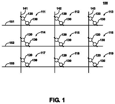
1 of 20 drawing sheets so far from the published document, cropped to the drawing. Every sheet is in the USPTO PDF.
What the patent claimed, word for word. All of it is now free to use.
The present invention relates to a nonvolatile latch circuit and a nonvolatile flip-flop circuit. Particularly, the present invention relates to a nonvolatile digital signal processing device which can restore a state of signal processing before a power supply is turned off, by a nonvolatile latch circuit restoring the state of the nonvolatile latch circuit which holds the state even when the power supply is turned off.
A great number of microcomputers and logic LSIs which include a digital circuit are used in electronic products.
In a digital circuit such as a microcomputer or an LSI, a latch circuit which temporarily holds digital signals for intermediate processed content, or a register circuit (hereinafter, collectively referred to as simply latch circuit) such as a flip-flop which stores one bit of digital information is used on a signal processing path. The latch circuit holds two states, high (H) and low (L) of a digital signal. As the simplest circuit configuration, a circuit configuration in which two inverter circuits are combined in a pair and mutually cross-connected to each other can be illustrated. In addition, a set-reset flip-flop (SR-FF) circuit in which two NAND circuits or two NOR circuits are combined in a pair and mutually cross-connected to each other, and an edge-triggered D flip-flop (D-FF) circuit in which a plurality of SR-FF circuits are combined, and the logic state of the output is updated in synchronization with clock edges can be also illustrated. Because these circuits are very ordinary known art, their detailed description is omitted. The operation speeds of the circuits are each determined by a turn-on time and a turn-off time of a transistor. Particularly, in an example of paired inverters, the operation speed is limited only by the switching speed of a C-MOS (Complementary-MOS) circuit including four MOSFETs (Metal Oxide Semiconductor Field Effect Transistor), and thus circuit operation on the order of nano seconds can be assured.
However, once the power source to the latch circuits is turned off, the state of each latch circuit is not held but is lost (volatile). In the case of a nonvolatile latch circuit in which the logic states of all latch circuits in a logic circuit are saved regardless of whether the power source is in ON state or OFF state, the logic states immediately before the turning off of the power source can be quickly restored when the power source is turned on again. Thus even when the power source for an electronic device is turned off by a user, the previous states can be fully restored when the power source is turned on again, thereby allowing continuous circuit operation without returning to the initial state.
Although power saving LSIs have been developed along with the progress of finer semiconductor process, limiting of leakage current has become difficult because of the progress, and thus the power saving LSIs in use of only finer semiconductor process are approaching the limit. For this reason, an approach to improving power saving is being adopted by elaborately controlling turning ON/OFF of the power source per circuit block within an LSI for unused circuit blocks. However, when the power source for a block is turned off, the logic state of the block is lost, and thus the approach cannot be performed on a circuit block for which continuous processing is needed. To the contrary, in the case where the above-described nonvolatile latch circuit constitutes all of the registers and latch circuits in logic circuits, a request for the continuous processing can be satisfied.
However, as an example of application to an LSI of a nonvolatile latch circuit in the conventional art, a floating gate memory element (hereinafter referred to as a flash memory) is utilized as a program recording memory of FPGA (Field-Programmable Gate Arrays) or FPLD (Field-Programmable Logic Devices), and thus the application is limited to a memory area formed as a separate area from a logic circuit. This is because erasing or writing information of or to a flash memory needs a time of the order of micro seconds (.mu.s), and thus the duty cycle of the flash memory cannot be synchronized with the duty cycle of the logic circuit. In the case where such a memory is individually installed in each latch circuit in the logic circuit, even when an operation of each latch circuit is completed, recording of information (logic state of the latch circuit) to the memory is not completed, and thus high-speed operation performance of the logic circuit is impaired. Consequently, in order to ensure high-speed operation of the logic circuit, the following processing is necessary: a flash memory is provided separately from the logic circuit; before the power source is turned off, the state in the logic circuit is transferred to the flash memory; and when the transfer is completed the power source is turned off. However, a problem arises that in the case of a sudden power off, all the latch states in the logic circuit cannot be transferred to the flash memory in time, and thus the recording cannot be completed. The voltage required for writing or erasing of a flash memory is generally substantially higher than the power source voltage of a logic circuit. Therefore, a write operation to the flash memory cannot be directly performed based on an output signal of the logic circuit. Consequently, the writing or erasing voltage of a flash memory needs to be supplied from the outside of an LSI or to be generated inside the LSI chip, and a dedicated driver circuit is necessary.
Furthermore, the manufacturing process of flash memory is complicated in general, and thus forming the logic circuit and the flash memory on the same substrate makes the process even more complicated. In addition, after the transistors that constitute the logic circuit are formed, high-heat process or the like is involved, and therefore the performance of the transistors may be impaired.
In order to cope with these problems, in recent years, the following proposals have been made to configure a nonvolatile latch circuit.
[First Conventional Embodiment]
First, as a first conventional embodiment, a nonvolatile latch circuit using a spin valve memory element as disclosed in PTL 1 is described. The spin valve memory element is also referred to as an MRAM (Magnetic Random Access Memory) cell, which is a memory element using Magneto Resistive Effect in which a resistance value changes in accordance with a magnetization direction. As the Magneto Resistive effect, Anisotropic Magnetoresistance (AMR), Giant Magnetoresistance (GMR), and Tunnel Magnetoresistance (TMR) are known.
FIG. 17A is a circuit configuration diagram of a nonvolatile latch circuit according to the first conventional embodiment. FIG. 17B is an operation timing chart of the nonvolatile latch circuit according to the first conventional embodiment. A nonvolatile latch circuit 600 illustrated FIG. 17A includes a sense latch circuit 601 and a write current generation circuit 602.
The sense latch circuit 601 includes an inverter circuit 611 which includes a p-type MOSFET 621 and an n-type MOSFET 622, an inverter circuit 612 which includes a p-type MOSFET 623 and an n-type MOSFET 624, p-type MOSFETs 625 and 626, an n-type MOSFET 627, and magnetoresistive elements MTJ0 and MTJ1. The write current generation circuit 602 has n-type MOSFETs 628 to 632.
In FIG. 17A, a data is inputted to IN terminal, and inverted data of IN terminal is inputted to IN (with an upper bar) terminal. In this state, when DATAGET terminal is set from "L" to "H" for a predetermined time period, as illustrated in FIG. 17B, the n-type MOSFET 632 is turned on, and a current i flows to DWL in a direction according to the input data. Accordingly, the resistances of the magnetoresistive elements MTJ0 and MTJ1 change, and one of them changes to a high resistance state and the other changes to a low resistance state. Subsequently, when REFRESHN terminal is set from "H" to "L" for a predetermined time period, the n-type MOSFET 627 is turned OFF, and the p-type MOSFETs 625 and 626 are turned ON. Accordingly, a node n1 and a node n2 are temporarily precharged to Vdd. The REFRESHN terminal is then set to "H" again, and the n-type MOSFET 627 is turned ON, and thus a current flows to GND via the magnetoresistive elements MTJ0 and MTJ1. The potentials of the node n1 and the node n2 gradually approach the GND potential because of the current. In this process, one of the magnetoresistive elements MTJ0 and MTJ1 that has less resistance value is discharged earlier and the corresponding node potential is reduced earlier. Consequently, the logic of a pair inverter circuit which includes the inverter circuits 611 and 612 converges, and the latch circuit is restored to the logic state according to the resistance relationship between the magnetoresistive elements MTJ0 and MTJ1.
Like this, PLT 1 states the effect that a nonvolatile latch circuit and a flip-flop circuit can be individually disposed in a logic circuit thanks to the nonvolatile latch circuit 600 using a magnetoresistive element, and the operation speed of the entire logic circuit is not impaired because high-speed rewrite to the magnetoresistive element is possible. PLT 1 also discloses that a high voltage which is different from the voltage necessary for a logic operation in rewriting to a memory element is unnecessary.
[Second Conventional Embodiment]
Next, as a second conventional embodiment, a nonvolatile latch circuit using a ReRAM (Resistive RAM) cell as disclosed in PLT1 is described. The ReRAM cell is a variable resistance element whose resistance value changes under application of an electrical stress (mainly electrical pulse). PLT 1 discloses an element in which a resistance film comprising ZnCdS is interposed between a silver (Ag) electrode and a platinum (Pt) electrode. The variable resistance element in this conventional embodiment changes to a high resistance state under application of a voltage which causes a current to flow from BE (Pt) electrode to TE (Ag) electrode, and exceeds a predetermined voltage level, or changes to a low resistance state under application of a voltage which causes a current to flow from TE (Ag) electrode to BE (Pt) electrode, and exceeds a predetermined voltage level. A nonvolatile latch circuit is configured by connecting the element as illustrated in FIG. 18.
FIG. 18 is a circuit configuration diagram of a nonvolatile latch circuit according to a second conventional embodiment. A nonvolatile latch circuit 700 illustrated in FIG. 20 includes variable resistance elements 711 and 712. The variable resistance element 711 and the variable resistance element 712 must be reset in a high resistance state. In a latch operation at normal operation time, Vctrl is pulled up to Vdd, and the variable resistance elements 711 and 712 are already in a high resistance state regardless of whether BL or BL_B is at the GND level or the Vdd level, and thus no resistance change occurs, and a normal latch operation is performed. Next, when the logic state of the latch circuit is stored in the variable resistance element, Vctrl is set to the GND level for a predetermined time period. Accordingly, the variable resistance element between BL and BL_B that is connected to "H" side changes to a low resistance state. The logic information of the latch circuit which has been stored as a low resistance state is restored in such a manner that when Vctrl is pulled up to Vdd, one of the variable resistance elements which is in a low resistance state is increased in potential earlier than the other variable resistance element, and consequently the side to which the variable resistance element in a low resistance state is connected converges to "H", and the other side converges to "L." In order to return to normal latch operation, it is necessary to reset the variable resistance element in a low resistance state to a high resistance state by increasing the potential of Vctrl terminal higher than Vdd because power consumption increases when a variable resistance element is in a low resistance state.
Thus, according to the example disclosed in PLT 1, a nonvolatile latch circuit can be achieved only by adding two variable resistance elements, and the speed of a normal latch operation is not impaired at all.
[Third Conventional Embodiment]
Next, as a third conventional embodiment, a nonvolatile latch circuit using a ReRAM cell disclosed in PLT 2 and PLT 3 is described.
FIG. 19 is a circuit image diagram illustrating a method of storing the state of a nonvolatile latch circuit according to the third conventional embodiment into a variable resistance element. FIG. 20 is a circuit diagram illustrating a method of restoring the previous latch state based on a resistance state stored in the variable resistance element in the nonvolatile latch circuit according to the third conventional embodiment. In the third conventional embodiment, two variable resistance elements are used as a pair for storing a latch state. A nonvolatile latch circuit 800 illustrated in FIG. 19 is a cross-coupled latch circuit such that an output terminal of an inverter circuit 821 is connected to an input terminal of an inverter circuit 822, and an output terminal of the inverter circuit 822 is connected to an input terminal of the inverter circuit 821. A variable resistance element 811 and a variable resistance element 812 are connected via node x and node y by switching a switch circuit (not shown).
When the nonvolatile latch circuit 800 has a state in which the node x in a High level and the node y is in a Low level, a current flows through the variable resistance elements 811 and 812 in the direction indicated by a voltage application direction A. Then the variable resistance element 811 changes to a state (referred to as HR state, or simply HR) in which a resistance value is high, and the variable resistance element 812 changes to a state (referred to as LR state, or simply LR) in which a resistance value is low.
When the nonvolatile latch circuit 800 has a state in which the node y in a High level and the node x is in a Low level, a current flows through the variable resistance elements 811 and 812 in the direction indicated by a voltage application direction B. Then the variable resistance element 811 changes to LR state and the variable resistance element 812 changes to HR state, and the states of the latch circuits are stored in the respective variable resistance elements.
On the other hand, by switching a switch circuit (not shown), the variable resistance elements 811 and 812 are connected to the power source lines of the inverter circuits 821 and 822 as illustrated in FIG. 20. In this circuit connection, in the case where the variable resistance element 811 is in HR and the variable resistance element 812 is in LR, when the power supply terminal A illustrated in FIG. 22 is pulled up from 0V to the power source voltage VDD, the current flowing through the inverter circuit 821 is reduced, and the current flowing through the inverter circuit 822 is increased. Accordingly, the output of the inverter circuit 821 rises up earlier than the output of the inverter circuit 822, and thus the node y is set to a High level, and the node x approaches a Low level so that the previous latch state is restored. Conversely, in the case where the variable resistance element 811 is in LR and the variable resistance element 812 is in HR, the current flowing through the inverter circuit 821 is increased, and the current flowing through the inverter circuit 822 is reduced. Accordingly, the output of the inverter circuit 822 rises up earlier than the output of the inverter circuit 821, and thus the node x is set to a High level, and the node y approaches a Low level so that the previous latch state is restored.
Thus, according to the configuration of the third conventional embodiment, an effect is obtained that the speed of a normal latch operation is not impaired at all even when a variable resistance element is separated from the latch circuit using a switch circuit. In addition, another effect is obtained that the durability of each variable resistance element can be significantly improved because after a resistance state is read from each variable resistance element, a voltage for causing the previous latch state to be restored is small, and a voltage stress is not applied to the variable resistance element after the restoring.
[Characteristics of Variable Resistance Element]
PTL 4 discloses the characteristic of the cellular structure of a variable resistance element, that is to say, the direction of voltage application and the direction of resistance change are determined as a consequence of configuring the oxide layers included in the variable resistance element in a stacked structure of a first oxide layer having a first oxygen content atomic percentage, and a second oxide layer having an oxygen content atomic percentage which is higher than that of the first oxide layer. PTL 5 discloses that the direction of voltage application and the direction of resistance change are determined as a consequence of utilizing two electrode materials whose standard electrode potentials are respectively high and low, the materials being used for the variable resistance element.
PTL 6 discloses that in some cases, it is necessary to limit the current for stable resistance change operation of a variable resistance element by connecting a load resistance to the variable resistance element in series and switching between the load characteristics of the load resistance in such a manner that the load resistance for changing to LR state is set to be higher than the load resistance for changing to HR state.
PTL 7 describes the possibility of a write failure such that a desired resistance cannot be reached in writing to a variable resistance element, and discloses additional writing after verification in which a write state is verified and additional writing is performed in the case where the write state is abnormal.
Patent Literature
[PTL 1] Japanese Unexamined Patent Application Publication No. 7, 2003-157671 [PTL 2] Japanese Unexamined Patent Application Publication No. 2008-85770 [PTL 3] WO 2009/060625 [PTL 4] WO 2008/149484 [PTL 5] WO 2009/050833 [PTL 6] WO 2006/137111 [PTL 7]
WO 2011/121971
Non Patent Literature
[NPL 1] "Nonvolatile SRAM Cell", IEEE 2006, 1-4244-0439-8/06
Technical Problem
Although, high-speed operation is described as an effect in the nonvolatile latch circuit of PTL 1 quoted as the first conventional embodiment, the speed of circuit operation is lower than that of a normal logic circuit because not only a switching delay of a MOSFET occurs between data input and data output, but also a write operation and a read operation to and from a magnetoresistive effect element are performed. Furthermore, because written information is read from an element, a glitch in which OUT and its inversion OUT (with an upper bar) are both set to "H" level may occur. Such a glitch may cause a malfunction once a logic circuit with synchronized clock is formed, and thus is undesirable. In addition, time division control is necessary, which uses 2 control lines for DATAGET which is a control signal for writing data, and REFRESHN which is a control signal for outputting (reading) data, and thus time allowance for DATAGET and REFRESHN operations needs to be considered, thereby preventing high-speed operation. Furthermore, rewriting to the variable resistance element is performed for each latch operation, and thus there is a concern that life of the variable resistance element may be reduced because of decreased durability for rewriting.
In the nonvolatile latch circuit of PTL 1 quoted as the second conventional embodiment, high-speed operation which is determined by the switching speed of transistors is possible because a circuit element for nonvolatile function has absolutely no influence on a normal latch operation. However, in order to store the state of the latch circuit, it is necessary to perform not only writing of the state to a variable resistance element, and a restore operation for reading the state from the variable resistance element, but also a reset operation for causing all variable resistance elements to change to a high resistance state. In the configuration where data input lines are pulled up by the variable resistance element, data input lines are inserted in the signal lines of all the latch circuits, and a current flows constantly through the data input lines, and thus there is a concern about an increase of power consumption. In order to perform reset operations for a great number of latch circuits at once, a powerful driver circuit is needed, which applies a voltage to a plurality of variable resistance elements in a low resistance state, and causes a current to flow through the variable resistance elements. Furthermore, in a normal latch operation, a voltage of Vdd is constantly applied to a variable resistance element connected to an input terminal at "L" level, and therefore an extremely high stress continues to be applied to the variable resistance element. In general, in a variable resistance element, for example, when a high resistance change voltage continues to be applied, the variable resistance element gradually changes to a higher resistance state than before. Accordingly, even when a voltage for changing the variable resistance element to a low resistance state in order to achieve a low resistance is applied to the variable resistance element subsequently, the variable resistance element is not likely to change to a low resistance state, that is to say, so-called resistance state imprinting phenomenon occurs.
In the latch circuit of PTL 2 and PTL 3 that are quoted as the third conventional embodiment, two variable resistance elements connected in series need to be rewritten, and thus as an application voltage, a voltage obtained by adding a voltage for changing to HR to a voltage for changing to LR is needed, thereby causing an adverse effect, such as an increase in the power source voltage of the latch circuit, and an increase in the number of the power source generation circuits. In a restore operation, when a plurality of latch circuits is powered on simultaneously in order to utilize the transient response in the power on, there is a concern that the power source voltage may be disturbed, which prevents stable restore operation.
Although current limiting needs to be performed in accordance with the direction of rewriting of a variable resistance element depending on the type of the variable resistance element as shown in PTL 6, there is no precedence example in which a specific solution is proposed for current limiting in a resistance change operation in a nonvolatile latch circuit using a variable resistance element. Particularly, in the case of the above-described third conventional embodiment, the amount of voltage distributed to the variable resistance element in HR state is more than the amount of voltage distributed to the other variable resistance element between the two variable resistance elements connected in series. For example, when the variable resistance element 811 is in HR state, and the variable resistance element 812 is in LR state in FIG. 19, most of applied voltage component is allocated to the variable resistance element 811 initially. When the variable resistance element 811 starts to change to LR state, part of the voltage component is distributed to the variable resistance element 812 accordingly. However, while the part of the voltage component is distributed to the variable resistance element 812, the voltage across both ends of the variable resistance element 811 reduces quickly, and a resistance change of the variable resistance element 811 may be interrupted before reaching normal LR state. That is to say, when one variable resistance element changes from HR state to LR state, the other variable resistance element in LR state serves as a load resistance, however, the resistance change to LR state may become unstable because the load resistance of the other variable resistance element also changes.
In the variable resistance element in PTL 7, when the resistance thereof is changed, a failure occurs in rare cases in which a write operation to a desired level cannot be performed. It is desirable to achieve a stable and reliable nonvolatile latch circuit which, even when such a write failure occurs, detects the write failure and performs additional writing after verification for rewriting data, and thus the write failure is restored.
In summary, any of the above-described conventional embodiments has a problem in increasing the speed of latch operation, expanding the life of the variable resistance element, reducing and stabilizing the operating voltage, and thus the above problems cannot be solved at the same time.
The present invention has been conceived in view of the above-mentioned problems, and it is an object of the invention to provide a nonvolatile latch circuit, a nonvolatile flip-flop circuit, and a nonvolatile signal processing device using those circuits which are able to perform storing and restoring of the state of a latch in a stable manner with a high speed and high reliability,
Solution to Problem
In order to solve the aforementioned problems, a nonvolatile latch circuit according to one aspect of the present invention includes: a latch operating unit including a first logic inversion circuit, and a second logic inversion circuit having an input terminal connected to an output terminal of the first logic inversion circuit and an output terminal connected to an input terminal of the first logic inversion circuit; a first transistor which includes a first terminal, a second terminal, and a first control terminal, and controls a conduction state between the first terminal and the second terminal in accordance with a voltage of the first control terminal; a second transistor which includes a third terminal, a fourth terminal, and a second control terminal, and controls a conduction state between the third terminal and the fourth terminal in accordance with a voltage of the second control terminal; and a variable resistance element having a structure in which an oxide layer comprising a metal oxide is interposed between first and second electrodes, wherein the first terminal of the first transistor and the first electrode of the variable resistance element are connected to each other via a first node, and the fourth terminal of the second transistor and the second electrode of the variable resistance element are connected to each other via a second node, the output terminal of the first logic inversion circuit and the second terminal of the first transistor are connected to each other via a third node, and the output terminal of the second logic inversion circuit and the third terminal of the second transistor are connected to each other via a fourth node, the variable resistance element changes to a first resistance state under application of a first write voltage higher than a first predetermined voltage, between the first electrode and the second electrode so as to cause a current to flow in a direction from the first electrode to the second electrode, and changes to a second resistance state which is higher in resistance value than the first resistance state under application of a second write voltage higher than a second predetermined voltage, between the first electrode and the second electrode so as to cause a current to flow in a direction from the second electrode to the first electrode, and the nonvolatile latch circuit further includes: a summing amplifier circuit which outputs a high-level voltage or a low-level voltage to the latch operating unit according to a value of sum of a potential at the first node and a potential at the second node so as to restore a logic state of the latch operating unit, the potentials being obtained by application of a voltage lower in absolute value than the first voltage and the second voltage to the first control terminal and the second control terminal, and the high-level voltage or the low-level voltage representing a resistance state of the variable resistance element; and a comparator circuit which outputs a high-level voltage or a low-level voltage based on a result of comparison for matching between an output of the summing amplifier circuit and an output of the first logic inversion circuit or the second logic inversion circuit when the summing amplifier circuit does not output the high-level voltage or the low-level voltage to the latch operating unit.
These comprehensive or specific aspects may be achieved as a system, a method, an integrated circuit, a computer program, or a recording medium such as a computer-readable CD-ROM, or as any combination of a system, a method, an integrated circuit, a computer program, and a recording medium.
Advantageous Effects of Invention
According to the configuration of the present invention, a nonvolatile latch circuit and a nonvolatile flip-flop circuit can be arbitrarily disposed in a logic circuit. The operation speed of the entire logic circuit to which the nonvolatile latch circuit and nonvolatile flip-flop circuit of the present invention are applied is only limited by the switching performance of the relevant transistors, and is not impaired at all by adding a nonvolatile function. When logic state information is recorded on a variable resistance element which is a memory element of a nonvolatile latch circuit or a nonvolatile flip-flop circuit, a high voltage which is used for a flash memory is not necessary. In addition, it is possible to check whether or not normal writing has been performed to the variable resistance elements incorporated in all circuit modules, and a write operation is not terminated with a write failure, and thus a desired latch state can be reliably stored. Thus, the present invention provides a highly stable nonvolatile latch circuit, nonvolatile flip-flop circuit, and nonvolatile signal processing device which can maintain stable data storing operation.
FIG. 1 is an element configuration diagram illustrating an example of the schematic configuration of a variable resistance element having a nonvolatile latch circuit according to Embodiment 1.
FIG. 2A is a graph illustrating an example of current-voltage characteristics of the variable resistance element according to Embodiment 1.
FIG. 2B is a diagram illustrating a voltage application state of negative voltage characteristics in the current-voltage characteristics of the variable resistance element shown in FIG. 2A.
FIG. 2C is a diagram illustrating a voltage application state of positive voltage characteristics in the current-voltage characteristics of the variable resistance element shown in FIG. 2A.
FIG. 3 is a circuit configuration diagram of the nonvolatile latch circuit according to Embodiment 1.
FIG. 4 is a block configuration diagram of the nonvolatile latch circuit according to Embodiment 1.
FIG. 5A is a diagram illustrating writing of HR state in a write (store) operation of the nonvolatile latch circuit according to Embodiment 1.
FIG. 5B is a diagram illustrating writing of LR state in a write (store) operation of the nonvolatile latch circuit according to Embodiment 1.
FIG. 6A is a circuit diagram illustrating a write operation to the variable resistance element in voltage application state B in FIG. 2C.
FIG. 6B is a circuit diagram illustrating a write operation to the variable resistance element in voltage application state A in FIG. 2B.
FIG. 7 is a graph in which a load resistance line of each transistor through which current flow is limited is superimposed on the voltage-current characteristics of the variable resistance element.
FIG. 8 is a block configuration diagram of a read (restore) operation for restoring a logic state of a latch circuit based on a resistance value stored in the variable resistance element in the nonvolatile latch circuit according to Embodiment 1.
FIG. 9A is a diagram illustrating a read operation when the variable resistance element is in HR state, node 1 is at a High level, and node 2 is at a Low level in the nonvolatile latch circuit according to Embodiment 1.
FIG. 9B is a diagram illustrating a read operation when the variable resistance element is in HR state, node 1 is at a Low level, and node 2 is at a High level in the nonvolatile latch circuit according to Embodiment 1.
FIG. 9C is a diagram illustrating a read operation when the variable resistance element is in LR state, node 1 is at a High level, and node 2 is at a Low level in the nonvolatile latch circuit according to Embodiment 1.
FIG. 9D is a diagram illustrating a read operation when the variable resistance element is in LR state, node 1 is at a Low level, and node 2 is at a High level in the nonvolatile latch circuit according to Embodiment 1.
FIG. 10A is a graph plotting normalized cell current values after write operations, in relation to the number of writes for a variable resistance element having inferior characteristics.
FIG. 10B is a graph plotting normalized cell current values after additional write operations, in relation to the number of writes for the variable resistance element.
FIG. 11 is a flowchart of a store operation performed by the nonvolatile latch circuit according to Embodiment 1.
FIG. 12 is a circuit configuration diagram of a nonvolatile latch circuit illustrating a modification of Embodiment 1.
FIG. 13 is a circuit configuration diagram of a nonvolatile latch circuit according to Embodiment 2.
FIG. 14 is a block diagram of the nonvolatile latch circuit according to Embodiment 2.
FIG. 15A is a circuit configuration diagram of a nonvolatile D flip-flop circuit according to Embodiment 3.
FIG. 15B is a block diagram of the nonvolatile D flip-flop circuit according to Embodiment 3.
FIG. 16 is a block diagram illustrating a configuration example of a nonvolatile signal processing device according to Embodiment 4.
FIG. 17A is a circuit configuration diagram of a nonvolatile latch circuit according to a first conventional embodiment.
FIG. 17B is an operation timing chart of the nonvolatile latch circuit according to the first conventional embodiment.
FIG. 18 is a circuit configuration diagram of a nonvolatile latch circuit according to a second conventional embodiment.
FIG. 19 is a schematic circuit configuration diagram illustrating a method of storing the state of a latch circuit according to a third conventional embodiment into a variable resistance element.
FIG. 20 is a circuit configuration diagram illustrating a method of restoring the previous latch state based on a resistance state stored in the variable resistance element in the latch circuit according to the third conventional embodiment.
Any of the above-described conventional nonvolatile latch circuits cannot solve the following problems at the same time.
Problem 1: the operation speed of each latch operation cannot be as high as the operation speed of a single latch circuit.
Problem 2: the life of each element is short because rewrite to the variable resistance element is performed for each latch operation.
Problem 3: the life of each element is short because voltage application is not made according to a voltage value and a time suitable for rewriting or reading.
Problem 4: the rewriting voltage cannot be reduced because a plurality of variable resistance elements are connected in series and thus application voltage for at least two elements is necessary.
Problem 5: the restore operation is unstable when transition period in which the power source voltage is increased is used in the restore operation.
Problem 6: resistance change process is unstable because current limiting is not performed when a resistance changes.
Problem 7: when the resistance of the variable resistance element is changed, a failure occurs in rare cases in which a write operation to a desired level cannot be performed. When such a write failure occurs, a written resistance state is not at a desired resistance level, and the restore operation for the latch circuit is unstable.
In order to solve the aforementioned problems, a nonvolatile latch circuit according to one aspect of the present invention includes: a latch operating unit including a first logic inversion circuit, and a second logic inversion circuit having an input terminal connected to an output terminal of the first logic inversion circuit and an output terminal connected to an input terminal of the first logic inversion circuit; a first transistor which includes a first terminal, a second terminal, and a first control terminal, and controls a conduction state between the first terminal and the second terminal in accordance with a voltage of the first control terminal; a second transistor which includes a third terminal, a fourth terminal, and a second control terminal, and controls a conduction state between the third terminal and the fourth terminal in accordance with a voltage of the second control terminal; and a variable resistance element having a structure in which an oxide layer comprising a metal oxide is interposed between first and second electrodes, wherein the first terminal of the first transistor and the first electrode of the variable resistance element are connected to each other via a first node, and the fourth terminal of the second transistor and the second electrode of the variable resistance element are connected to each other via a second node, the output terminal of the first logic inversion circuit and the second terminal of the first transistor are connected to each other via a third node, and the output terminal of the second logic inversion circuit and the third terminal of the second transistor are connected to each other via a fourth node, the variable resistance element changes to a first resistance state under application of a first write voltage higher than a first predetermined voltage, between the first electrode and the second electrode so as to cause a current to flow in a direction from the first electrode to the second electrode, and changes to a second resistance state which is higher in resistance value than the first resistance state under application of a second write voltage higher than a second predetermined voltage, between the first electrode and the second electrode so as to cause a current to flow in a direction from the second electrode to the first electrode, and the nonvolatile latch circuit further includes: a summing amplifier circuit which outputs a high-level voltage or a low-level voltage to the latch operating unit according to a value of sum of a potential at the first node and a potential at the second node so as to restore a logic state of the latch operating unit, the potentials being obtained by application of a voltage lower in absolute value than the first voltage and the second voltage to the first control terminal and the second control terminal, and the high-level voltage or the low-level voltage representing a resistance state of the variable resistance element; and a comparator circuit which outputs a high-level voltage or a low-level voltage based on a result of comparison for matching between an output of the summing amplifier circuit and an output of the first logic inversion circuit or the second logic inversion circuit when the summing amplifier circuit does not output the high-level voltage or the low-level voltage to the latch operating unit.
The description continues in the full USPTO document.
About 6,500 words. The USPTO PDF has it with every drawing.
Fees are due 3.5, 7.5 and 11.5 years after grant. This patent expired on July 29, 2026, so the fee marked "not paid" was the one that went unpaid.
NONVOLATILE LATCH CIRCUIT, NONVOLATILE FLIP-FLOP CIRCUIT, AND NONVOLATILE SIGNAL PROCESSING DEVICE
Filed Nov 2012 · published Mar 2014Nonvolatile latch circuit, nonvolatile flip-flop circuit, and nonvolatile signal processing device
Filed Nov 2012 · granted Jul 2014Earlier publications, parents and continuations. None of them can still be enforced, or this patent would not be listed.
Prior art cited by the examiner or applicant. Useful when you check your own idea for novelty.
Everything on this page comes from the documents linked above.