Background
The present technology relates to a solid-state imaging device and an electronic apparatus including the solid-state imaging device.
There is a CMOS (Complementary Metal Oxide Semiconductor) solid-state imaging device as one solid-state imaging device which is used in electronic apparatuses such as digital still cameras, digital video cameras, or the like.
The CMOS solid-state imaging device includes a semiconductor substrate which is formed of silicon, or the like, and includes a pixel region in which a plurality of pixels is arranged, for example, in a matrix shape, on the semiconductor substrate. Each pixel which is arranged in the pixel region is configured by a photodiode as a light receiving element having a photoelectric conversion function, and a plurality of MOS transistors.
In the CMOS solid-state imaging device, a wiring layer in which, for example, a plurality of wirings is laminated inter layers through an insulating film is provided on one plate surface of the semiconductor substrate. In addition, the CMOS solid-state imaging device has a color filter layer, and a plurality of micro lenses on the side where the semiconductor substrate is irradiated with light.
The color filter layer is divided into a plurality of color filters for each photodiode which configures each of the pixels. Each of the color filters is a filter portion of any color of, for example, red, green, and blue, and transmits light of each color component. A micro lens is formed for each pixel, corresponding to the photodiode configuring each pixel. The micro lens condenses the input light from the outside to a photodiode of corresponding pixel.
For the CMOS solid-state imaging device with the above described configuration, there are a so-called front side illumination type and a backside illumination type. The front side illumination and the backside illumination are different from each other, since the input side of light with respect to the semiconductor substrate having the wiring layer on one plate surface side is the front side for the front side illumination, and the rear side for the backside illumination.
Specifically, in the front side illumination CMOS solid-state imaging device, the color filter layer and the micro lens are formed through the wiring layer which is provided on one side of the semiconductor substrate with respect to the semiconductor substrate. That is, in the structure of the front side illumination, the wiring layer is provided on the side where the light is input with respect to the semiconductor substrate.
On the contrary, in the backside illumination CMOS solid-state imaging device, the color filter layer and the micro lens are formed on the side opposite to the side where the wiring layer is provided with respect to the semiconductor substrate. That is, in the structure of the backside illumination, the wiring layer is provided on the side opposite to the side where the light is input with respect to the semiconductor substrate.
Due to the above described difference in the structure of the front side illumination and the backside illumination, there are operational differences between both as follows. In a case of the front side illumination, the light which is input from the micro lens side transmits the color filter layer, passes through the inside of the wiring layer, and then is received by the photodiode of each pixel which configures the pixel region.
In contrast to this, in a case of the backside illumination, the light which is input from the micro lens side passes through the color filter layer, and is received by the photodiode of the pixel without passing through the wiring layer. For this reason, according to the structure of the backside illumination, since the light which is input from the micro lens side is received by the photodiode of the pixel without being blocked by the wiring layer, it is possible to secure the actual light receiving area of the photodiode widely, and to improve the sensitivity thereof.
However, there is a problem in the Back side illumination CMOS solid-state imaging device as follows, since the wiring layer is not present on the side where the light is input with respect to the semiconductor substrate. First, in the structure of the backside illumination, it is very difficult to suppress optical color mixing completely. Here, the optical color mixing is a phenomenon in which, in a border portion of pixels where pixels with different colors from each other are close to each other, a part of light which is input to the micro lens corresponding to pixels of one color is input to the photodiode of pixels of the other color.
In addition, in the Back side illumination CMOS solid-state imaging device, for example, when a high intensity light source such as the sun or the like is photographed, there may be a magenta colored stripe shaped pixel defect (hereinafter, referred to as "Mg flare") which is referred to as magenta flare, or the like. The Mg flare occurs as follows.
A part of the light which is input from the micro lens toward the photodiode side of the pixel becomes light which goes toward the micro lens side from the photodiode side as reflected light or diffracted light. The reflected light or the diffracted light passing through the micro lens, or the like, is reflected by seal glass which covers the micro lens, or the like, in the package of the CMOS solid-state imaging device, and is input from the micro lens again toward the photodiode side. The light which is input to the photodiode side again in this manner causes the optical color mixing to uniformly occur in pixels of each color of, for example, red, green, and blue.
In addition, in the CMOS solid-state imaging device, processing, which is referred to as white balance processing, is performed so as to arrange spectral characteristics of light of each color component, in the process of signal processing. According to the white balance processing, for example, when the color filter layers are divided into three color filters of red, green, and blue, the red and blue signals have a larger gain than the green signal, and are emphasized. The Mg flare occurs due to such a white balance processing which is performed in a state where each color pixel is uniformly mixed, as described above.
In order to solve the problem in the above described backside illumination structure, the technology described in Japanese Unexamined Patent Application Publication No. 2010-186818 has been proposed, and has come into practical use. In the technology in Japanese Unexamined Patent Application Publication No. 2010-186818, a light shielding film is formed through an insulating layer in the pixel boundary on the light receiving surface of the photodiode, that is, between the adjacent pixels, in between the semiconductor substrate on which the photodiode is formed and the color filter layer.
The technology in Japanese Unexamined Patent Application Publication No. 2010-186818 is considered to be reliably effective when it comes to suppressing the above described optical color mixing and Mg flare. However, according to the technology in Japanese Unexamined Patent Application Publication No. 2010-186818, the sensitivity may be decreased, since a part of the light to be sensed by the pixel is blocked due to the light shielding film which is formed between the adjacent pixels. The degree of decrease in sensitivity due to the light shielding film which is formed between the adjacent pixels depends on the pixel pitches between the pixels in the CMOS solid-state imaging device, the line width of the light shielding film, a light condensing structure, or the like, however, there is a case where the sensitivity is decreased by about 10% in practice due to the light shielding film.
Therefore, in order to suppress such a decrease in sensitivity due to the light shielding film which is formed between the adjacent pixels, the technology described in Japanese Unexamined Patent Application Publication No. 2010-109295 has been proposed. The technology described in Japanese Unexamined Patent Application Publication No. 2010-109295 focuses on an electrostatic light shielding effect due forming the light shielding film from a metallic material, and forms the light shielding film using a non-conductive material such as amorphous silicon.
Summary
According to the technology in Japanese Unexamined Patent Application Publication No. 2010-109295, it is considered that the decrease in sensitivity due to the electrostatic light shielding effect may be reliably suppressed by using the non-conductive material in the light shielding film. However, even in the technology in Japanese Unexamined Patent Application Publication No. 2010-109295, the effect of suppressing the decrease in sensitivity is limited due to the fact that the light to be sensed by the pixel is blocked because of the light shielding film.
It is desirable to provide a solid-state imaging device and an electronic apparatus in which optical color mixing, or Mg flare is suppressed, and sensitivity is improved.
According to an embodiment of the present technology, there is provided a solid-state imaging device which includes, a pixel region which is provided on a semiconductor substrate, and in which a plurality of pixels including a photoelectric conversion unit having a photoelectric conversion function is arranged; a wiring layer which is provided at one plate surface of the semiconductor substrate; a color filter layer which is divided into a plurality of color filters provided corresponding to each pixel of the plurality of pixels which is arranged in the pixel region; and an inter-pixel light shielding unit which is provided in a boundary portion between the pixels adjacent to each other, between the semiconductor substrate and the color filter layer, in which the plurality of pixels has a combination of different color pixels in which the colors of the color filter are different from each other, and a combination of the same color pixels in which the colors of the color filter are the same as each other, as the pixels which are adjacent to each other, due to the color of the color filter, and the inter-pixel light shielding units are biasedly located at the boundary portion of the combination of the different color pixels.
In addition, in the solid-state imaging device according to the present technology, the wiring layer and the color filter layer may be provided on a different plate surface side from each other with respect to the semiconductor substrate, and the inter-pixel light shielding unit may be a light shielding film.
In addition, the solid-state imaging device according to the present technology may further include, a peripheral circuit region which is provided at the periphery of the pixel region; and a peripheral light shielding film which is provided at the peripheral circuit region in between the semiconductor substrate and the color filter layer, and is located at the same layer as the light shielding film.
In addition, in the solid-state imaging device according to the present technology, the light shielding film may only be present at the boundary portion of the combination of the different color pixels, without being present at the boundary portion of the combination of the same color pixels.
In addition, in the solid-state imaging device according to the present technology, the light shielding film may be connected to a fixed potential.
In addition, in the solid-state imaging device according to the present technology, the plurality of light shielding films which is present at the boundary portion of the plurality of pixels may be electrically connected to each other by a transparent electrode.
In addition, in the solid-state imaging device according to the present technology, the wiring layer and the color filter layer may be provided at the same plate surface as each other with respect to the semiconductor substrate, and the inter-pixel light shielding unit is a wiring which configures the wiring layer.
In addition, the solid-state imaging device according to the present technology may further include, a signal processing circuit which performs processing of an output signal from each of the pixels, in which the signal processing circuit corrects an output value of the output signal from each of the pixels on the basis of the magnitude of a difference in sensitivity which occurs between the plurality of pixels due to a difference in the amount of the inter-pixel light shielding unit at the boundary portion which is present in the periphery of each of the pixels.
According to another embodiment of the present technology, there is provided an electronic apparatus which includes, a solid-state imaging device; and a drive unit which generates a driving signal for driving the solid-state imaging device, in which the solid-state imaging device includes, a pixel region which is provided on a semiconductor substrate, and in which a plurality of pixels including photoelectric conversion unit having a photoelectric conversion function is arranged; a wiring layer which is provided at one plate surface of the semiconductor substrate; a color filter layer which is divided into a plurality of color filters provided corresponding to each pixel of the plurality of pixels which is arranged in the pixel region; and an inter-pixel light shielding unit which is provided in a boundary portion between the pixels adjacent to each other, between the semiconductor substrate and the color filter layer, in which the plurality of pixels has a combination of different color pixels in which the colors of the color filter are different from each other, and a combination of the same color pixels in which the colors of the color filter are the same as each other, as the pixels which are adjacent to each other, due to the color of the color filter, and the inter-pixel light shielding units are biasedly located at the boundary portion of the combination of the different color pixels.
The electronic apparatus according to the present technology may further include, a shutter device for controlling an irradiation time and a light blocking time of light with which irradiates the solid-state imaging device, in which the drive unit corrects an output value of an output signal from each of the pixels on the basis of the magnitude of a difference in sensitivity which occurs between the plurality of pixels due to a difference in the amount of the inter-pixel light shielding unit at the boundary portion which is present in the periphery of each of the pixels.
According to the present technology, it is possible to suppress optical color mixing, or Mg flare, and to improve sensitivity.
Brief description of the drawings
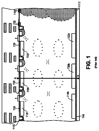
FIG. 1 is a diagram which shows a schematic configuration of a solid-state imaging device according to a first embodiment of the present technology.
FIG. 2 is a diagram which shows a detailed configuration of the solid-state imaging device according to the first embodiment of the present technology.
FIG. 3 is a diagram which shows an example of pixel array of the solid-state imaging device according to the first embodiment of the present technology.
FIG. 4 is an explanatory diagram of an operation of the solid-state imaging device according to the first embodiment of the present technology.
FIG. 5 is an explanatory diagram of the operation of the solid-state imaging device according to the first embodiment of the present technology.
FIG. 6 is a cross-sectional view which shows a configuration of the solid-state imaging device according to a second embodiment of the present technology.
FIG. 7 is a cross-sectional view which shows a configuration of the solid-state imaging device according to a third embodiment of the present technology.
FIG. 8 is a plan view which shows a configuration of the solid-state imaging device according to the third embodiment of the present technology.
FIG. 9 is a plan view which shows the configuration of the solid-state imaging device according to the third embodiment of the present technology.
FIG. 10 is a plan view which shows a configuration of the solid-state imaging device according to a fourth embodiment of the present technology.
FIG. 11 is a cross-sectional view which shows a configuration of the solid-state imaging device according to a fifth embodiment of the present technology.
FIG. 12 is a cross-sectional view which shows a configuration of the solid-state imaging device according to a sixth embodiment of the present technology.
FIG. 13 is a plan view which shows the configuration of the solid-state imaging device according to the sixth embodiment of the present technology.
FIG. 14 is a plan view which shows the configuration of the solid-state imaging device according to the sixth embodiment of the present technology.
FIG. 15 is a plan view which shows a configuration of the solid-state imaging device of a comparison example of the present technology.
FIG. 16 is a diagram which shows a configuration of an electronic apparatus according to a first embodiment of the present technology.
FIGS. 17A to 17D are diagrams which show examples of pixel arrays as an application example of the present technology.
FIG. 18 is a diagram which shows an example of the pixel array as an application example of the present technology.
FIG. 19 is a diagram which shows an example of the pixel array as an application example of the present technology.
FIG. 20 is a diagram which shows an example of the pixel array as an application example of the present technology.
Detailed description of embodiments
The present technology is to improve the sensitivity while suppressing the optical color mixing and the Mg flare by studying a layout of the inter-pixel light shielding unit which is provided at the boundary portion between the pixels which are adjacent to each other, in between the semiconductor substrate on which the plurality of pixels is arranged and the color filter layer which is divided into a plurality of color filters which is provided corresponding to each pixel.
Schematic Configuration of Solid-State Imaging Device
The configuration of a solid-state imaging device 1 according to a first embodiment of the present technology will be described with reference to FIG. 1. The solid-state imaging device 1 according to the embodiment is a CMOS solid-state imaging device. The solid-state imaging device 1 has a semiconductor substrate 2 which is configured by a semiconductor such as silicon. The solid-state imaging device 1 includes a pixel region 3, and a peripheral circuit region 4 which is provided at the periphery of the pixel region 3.
The pixel region 3 is an image capturing area which is provided on the semiconductor substrate 2, and includes a plurality of pixels 5 which is provided in a predetermined array. The pixel region 3 includes an effective pixel region where a generation, an amplification, and reading out of a signal charge using photoelectric conversion in each pixel 5 is performed, and an optical black level region where optical black as the reference of a black level is output. In general, the optical black level region is formed at the outer periphery of the effective pixel region.
In the solid-state imaging device 1 according to the embodiment, the plurality of pixels 5 is arranged according to a so-called clear bit sequence, and is arranged in a diagonal matrix in a state of being diagonal by 45.degree. with respect to the semiconductor substrate 2 having a rectangular shape when planarly viewed. The pixel 5 is formed on the semiconductor substrate 2. Since the clear bit sequence is used, as the array of the plurality of pixels 5 (hereinafter, referred to as "pixel array"), it is easy to secure a wide area of one pixel while maintaining a resolution.
In the solid-state imaging device 1 according to the embodiment, the clear bit sequence is used as the pixel array, however, the pixel array is not particularly limited. For example, a general square grid array may be adopted, in which the plurality of pixels 5 is arranged in a matrix in the longitudinal direction (orthogonal direction), or transverse direction (horizontal direction) planarly along the rectangular semiconductor substrate 2.
The pixel 5 is configured by a photodiode as the photoelectric conversion unit having the photoelectric conversion function, and a plurality of MOS transistors. The photodiode which configures the pixel 5 has a light receiving surface, and generates a signal charge of an amount corresponding to the intensity of input light. The pixel 5 has a transistor, for example, which takes in charge of amplifying, transmitting, selection, and resetting of the signal charge which is generated by the photodiode, respectively, as the plurality of MOS transistor.
The peripheral circuit region 4 includes a first driving circuit 6, a column signal processing circuit 7, a second driving circuit 8, an output circuit 9, and a control circuit 10.
The first driving circuit 6 is configured by, for example, a shift register, and drives the plurality of pixels 5 in the matrix which is diagonal by 45.degree. in the sequence of a first direction (refer to arrow A1) as the arrangement direction corresponding to the row direction, or the column direction in the matrix arrangement. The first driving circuit 6 is connected by a pixel driving wiring with respect to the plurality of pixels 5.
The first driving circuit 6 supplies a driving pulse for driving the pixel 5 to the selected pixel driving wiring, by selecting the pixel driving wiring, and drives the pixel in the sequence of the first direction. The first driving circuit 6 sequentially selects and scans each pixel 5 in the pixel region 3 in the first direction, in the sequence of the first direction, and supplies a pixel signal based on the signal charge which is generated in the photodiode of each pixel 5 to the column signal processing circuit 7 through a predetermined signal line.
The column signal processing circuit 7 is a signal processing circuit which performs the processing of the output signal from each pixel 5. The column signal processing circuit 7 has elements for each sequence in a second direction which is orthogonal to the first direction in the arrangement direction corresponding to the row direction, or the column direction, in the matrix arrangement of the plurality of pixel 5. The column signal processing circuit 7 processes a signal which is output from the pixel 5 of one unit of the sequence in the first direction for each of the pixel 5 groups in the sequence of the second direction, using each element.
For the signal processing performed by the column signal processing circuit 7, there are, for example, CDS (Correlated Double Sampling) for reducing specific fixed pattern noise for each pixel 5, signal amplifying, AD (analog/digital) conversion, or the like. A selection switch (not shown) is provided at an output stage of the column signal processing circuit 7.
The second driving circuit 8 is configured by, for example, the shift register, sequentially selects each element of the column signal processing circuit 7 by sequentially outputting a scanning pulse in the second direction, and outputs the pixel signal to a predetermined signal line 11 from each element of the column signal processing circuit 7.
The output circuit 9 outputs a signal which is sequentially supplied through the signal line 11 from each element of the column signal processing circuit 7, by performing a predetermined signal processing. As the signal processing which is performed by the output circuit 9, for example, there are buffering, a black level adjustment, column dispersion compensation, various digital processing, or the like.
The control circuit 10 receives data for instructing an operation mode or the like, input clock, or the like, or outputs data such as internal information of the solid-state imaging device 1. The control circuit 10 generates the clock signal as the reference of operations of the first driving circuit 6, the column signal processing circuit 7, and the second driving circuit 8, or the control signal, and inputs the generated signal to each of the circuits 6, 7, and 8, on the basis of a synchronous signal and master clock in each of the first and second directions in the pixel array.
Detailed Configuration of Solid-State Imaging Device
Detailed configuration of the solid-state imaging device 1 will be described. The solid-state imaging device 1 is a backside illumination CMOS solid-state imaging device. As shown in FIG. 2, the solid-state imaging device 1 has the pixel region 3 which is provided on the semiconductor substrate 2. The pixel region 3 is a region where the pixels 5 including a photodiode 21 as the photoelectric conversion unit having the photoelectric conversion function are arranged in plural.
The pixel 5 includes the photodiode 21 and the MOS transistor 22. The photodiode 21 is formed in the entire region of the semiconductor substrate 2 in the thickness direction. According to the embodiment, the photodiode 21 includes an n-type semiconductor region 23 as a first conductive type, and a p-type semiconductor region 24 as a second conductive type which is formed so as to face both the front and rear surface sides of the semiconductor substrate 2, and is configured as p-n junction type photodiode. The p-type semiconductor region 24 included in the photodiode 21 serves as a hole charge storage area, as well.
The MOS transistor 22 has a source/drain region (not shown), and a gate electrode 25. The source/drain region of the MOS transistor 22 is formed in a p-type semiconductor well region 26 which is formed on the surface 2a side as one plate surface side of the semiconductor substrate 2, as an n-type region. The gate electrode 25 is formed on the surface 2a of the semiconductor substrate 2 in between both regions of the source/drain region of the MOS transistor 22 through a gate insulation film.
Each of the pixels 5 which is formed of the photodiode 21 and the MOS transistor 22 are separated by an element isolation region 27. The element isolation region 27 is formed as the p-type semiconductor region, and is grounded.
A laminated wiring layer 28 is provided on the surface side 2a of the semiconductor substrate 2. The laminated wiring layer 28 has a plurality of wirings 30 which is laminated through an interlayer insulation film 29. The interlayer insulation film 29 is configured by, for example, a silicon oxide film which is formed of silicon dioxide (SiO.sub.2). The plurality of wirings 30 is formed of, for example, different metal, and is connected to each other through a plug or the like which is formed between layers. In addition, according to the embodiment, the wiring layer which is provided on one plate surface side of the semiconductor substrate 2 is the laminated wiring layer 28 having the plurality of wirings, however, the wiring layer is not limited to this, and may be a wiring layer of a single layer structure.
On the other hand, an insulation film 31 which functions as an antireflection film is provided on the rear surface 2b as the other plate surface of the semiconductor substrate 2. The insulation film 31 has a laminated structure in which a plurality of films with different refractivity from each other is laminated. According to the embodiment, the insulation film 31 has a two-layer structure which is formed of a silicon oxide film 32 which is laminated from the semiconductor substrate 2 side, and a hafnium oxide film 33.
In addition, in the pixel region 3, a planarizing film 34 with optical transparency is provided on the insulation film 31. The planarizing film 34 is, for example, formed of an organic material such as resin. A color filter layer 35 is formed on the planarizing film 34. A plurality of micro lenses 36 is formed on the color filter layer 35.
The color filter layer 35 is divided into a plurality of color filters 37 which is provided corresponding to each pixel 5 of the plurality of pixels 5 which is arranged in the pixel region 3. That is, the color filter layer 35 is divided into the plurality of color filters 37 for each photodiode 21 which configures each pixel 5.
In the solid-state imaging device 1 according to the embodiment, each of the color filters 37 is a filter portion of any one of colors of red (R), green (G), and blue (B), and transmits light of each color component. The color filter 37 of each color is so-called an on-chip color filter, and is formed according to the clear bit sequence.
The micro lens 36 is so-called on-chip micro lens, and is formed for each pixel 5 corresponding to the photodiode 21 which configures the pixel 5. Accordingly, the plurality of micro lenses 36 is arranged in a matrix planarly, similarly to the pixel 5. The micro lens 36 condenses light which is input from the outside to the photodiode 21 of the corresponding pixel 5. The micro lens 36 is formed of, for example, the organic material such as resin.
In addition, in the solid-state imaging device 1 according to the embodiment, an inter-pixel light shielding film 40 as an inter-pixel light shielding unit is provided on the pixel boundary in the planarizing film 34 which is formed on the insulation film 31. The inter-pixel light shielding film 40 is a light shielding film which is formed on the insulation film 31 along the boundary line between the pixels 5 adjacent to each other. That is, the inter-pixel light shielding film 40 is formed as a linear layer portion having a predetermined line width with respect to the pixel 5 with a substantially rectangular shape, along the side of the substantially rectangular shape, when planarly viewed.
The inter-pixel light shielding film 40 is formed of a material which blocks off light. As a material forming the inter-pixel light shielding film 40, it is preferable to use a material with a strong light blocking effect, and is suitable for micromachining, for example, so as to be processed accurately using etching. As the material having such a property, for example, there is metal of aluminum (Al), tungsten (W), copper (Cu), or the like.
The inter-pixel light shielding film 40 is formed on the insulation film 31 using a method including a deposition process for forming film using metal materials of aluminum or the like described above, a mask process which selectively forms a resist mask on the metal layer which is formed using the deposition process, and a removal process for selectively removing the metal layer through the resist mask.
In the deposition process, for example, a spattering method, CVD (Chemical Vapor Deposition) method, plating, or the like are used, and a film (metal layer) is formed using the metal material of the above described aluminum or the like. In the mask process, the resist mask is formed along a portion corresponding to the boundary between the plurality of pixels 5. In the removal process, the metal layer is selectively removed using the etching of wet etching, dry etching, or the like.
As described above, the solid-state imaging device 1 according to the embodiment has a backside illumination structure in which the color filter layer 35 and the micro lens 36 are provided on the rear surface 2b side which is the opposite side to the front surface 2a side on which the laminated wiring layer 28 is provided with respect to the semiconductor substrate 2. That is, in the solid-state imaging device 1, the laminated wiring layer 28 and the color filter layer 35 are provided on the plate surfaces which are different from each other with respect to the semiconductor substrate 2, and the laminated wiring layer 28 is provided on the front surface 2a side which is opposite to the rear surface 2b side to which light is input with respect to the semiconductor substrate 2.
In the backside illumination solid-state imaging device 1, the light which is input from the micro lens 36 side transmits the color filter layer 35, and is received by the photodiode 21 of the pixel 5 without passing through the laminated wiring layer 28. For this reason, in the solid-state imaging device 1, the light which is input from the micro lens 36 side is received by the photodiode 21 of the pixel 5 without being blocked by the laminated wiring layer 28, accordingly, it is easy to secure an actual light receiving area of the photodiode 21, and is able to obtain a relatively high sensitivity, in contrast to a so-called front side illumination structure. In addition, since the laminated wiring layer 28 is provided on the front surface 2a side as the opposite side to the side (the rear surface 2b side) where the light is input with respect to the semiconductor substrate 2, it is possible to obtain high degree of freedom with respect to a layout of the wiring 30 which configures the laminated wiring layer 28.
In addition, the solid-state imaging device 1 according to the embodiment includes the inter-pixel light shielding film 40 as the inter-pixel light shielding unit which is provided at the boundary portion (hereinafter, referred to as "inter-pixel boundary portion") between the pixels 5 adjacent to each other, between the semiconductor substrate 2 and the color filter layer 35. Specifically, the solid-state imaging device 1 has the inter-pixel light shielding film 40 on the insulation film 31 which is provided between the rear surface 2b side of the semiconductor substrate 2 and the color filter layer 35.
In addition, the solid-state imaging device 1 according to the embodiment is the backside illumination, however, the device may be a front side illumination solid-state imaging device in which the laminated wiring layer 28 is provided on the front surface 2a side to which the light is input with respect to the semiconductor substrate 2. When it is the backside illumination structure, the color filter layer 35 and the micro lens 36 are formed on the same side as the laminated wiring layer 28 through the laminated wiring layer 28 which is provided on one side of the semiconductor substrate 2 with respect to the semiconductor substrate 2. In this manner, the laminated wiring layer 28 included in the solid-state imaging device 1 may be provided on any one plate surfaces side of the semiconductor substrate 2.
When the solid-state imaging device 1 has the front side illumination structure, for example, the insulation film such an insulation film 31 is formed on the laminated wiring layer which is provided on one surface side of the semiconductor substrate 2, and the inter-pixel light shielding film 40 is provided on the insulation film. However, in any of the front side illumination and the backside illumination, the position where the inter-pixel light shielding film 40 is provided is not particularly limited, if the position is a portion between the semiconductor substrate 2 and the color filter layer 35 in the solid-state imaging device 1.
Detailed Configuration of Inter-Pixel Light Shielding Film
A configuration of the inter-pixel light shielding film 40 included in the solid-state imaging device 1 according to the embodiment will be described in detail. As described above, in the pixel array, the inter-pixel light shielding film 40 which is provided at the inter-pixel boundary portion is selectively provided on the basis of the relationship of the colors of the color filter 37 (hereinafter, referred to as "color" simply) of a pair of pixels 5 which configures the boundary by being adjacent to each other. That is, the inter-pixel light shielding film 40 is provided at a part of the inter-pixel boundary portion, on the basis of the color combination of the pixels 5 which are adjacent to each other, among all the inter-pixel boundary portions, in the pixel region 3 in which the plurality of pixels 5 are arrayed.
Here, the pixel array included in the solid-state imaging device 1 according to the embodiment will be described with reference to FIG. 3. As shown in FIG. 3, the pixel array in the pixel region 3 is the above described clear bit sequence, and is arranged in a diagonal matrix in a state of being diagonal by 45.degree. with respect to the semiconductor substrate 2 having a rectangular shape when planarly viewed. In FIG. 3, red, green, and blue are represented by "R", "G", and "B", respectively, for the color of each of pixels 5.
As shown in FIG. 3, in the clear bit sequence, in each direction of the first direction (refer to arrow A1) and the second direction (refer to arrow A2), pixel columns 41 which are formed only of green (G) pixel 5 (hereinafter, referred to as "G pixel") (hereinafter, referred to as "single color pixel column"), and pixel columns 42 which are formed of three color pixels 5 (hereinafter, referred to as "multicolor pixel column") of red (R) pixel 5 (hereinafter, referred to as "R pixel"), blue (B) pixel 5 (hereinafter, referred to as "B pixel"), and G pixel are alternately arranged. In the multicolor R pixel column 42, the R pixel and the B Pixel are alternately arranged by interposing the G Pixel therebetween.
In this clear bit sequence, as color combinations of pixels 5 which are adjacent to each other, there are a color combination of the pixel 5 in which colors are different from each other, and a color combination of the pixel 5 in which colors are the same as each other.
Specifically, in the clear bit sequence shown in FIG. 3, in each direction of the first direction and the second direction, the combination of the multicolor pixels is formed by any of combinations of the R pixel and G pixel, or the G pixel and B pixel which are adjacent to each other, regarding the pixels 5 configuring the multicolor pixel column 42. In addition, in each direction of the first direction and the second direction, the pixels adjacent to each other forms the same color pixel combination with only the G Pixels, regarding the pixels 5 configuring the single color pixel column 41.
In this manner, in the solid-state imaging device 1 according to the embodiment which adopts the clear bit array as the pixel array, the plurality of pixels 5 has the combination of different color pixels of which colors of the color filter 37 are different from each other, and the combination of the same color pixels of which colors of the color filter 37 are the same as each other, as the pixels 5 adjacent to each other, using the colors of the color filter 37.
Hereinafter, pixels 5 which are adjacent to each other in the combination of the different color pixels are referred to as "inter-pixel of different colors", and the pixels 5 which are adjacent to each other in the combination of the same color pixels are referred to as "inter-pixel of the same colors". That is, in the above described clear bit sequence, as the inter-pixel of different colors, there are inter-pixel of R pixel and G pixel, and the inter-pixel of G pixel and B pixel, and as the inter-pixel of the same colors, there are inter-pixel of G pixels.
In addition, in the solid-state imaging device 1 according to the embodiment, the inter-pixel light shielding film 40 is provided so as to be concentrated at the pixel boundary portion in the different color combination, that is, at the boundary portion between the different color pixels, in the above described clear bit sequence.
The description continues in the full USPTO document.
 Lapsed, fee not paid13 drawings