Background of the invention
1. Field of the invention
The present invention relates to a solid-state imaging device and a method for manufacturing the same, and to an electronic apparatus including the solid-state imaging device, such as a camera, and to a camera module.
2. Description of the related art
Solid-state imaging devices (image sensors) include CCD image sensors that include a charge-coupled device (CCD) for read-out signal charges, and CMOS image sensors in which each pixel includes one photoelectric conversion portion and a plurality of pixel transistors. These are used in a variety of portable terminal apparatuses, such as digital still cameras, digital video cameras, and cellular phones with a camera.
A CCD image sensor includes two-dimensionally arranged light-receiving portions acting as photoelectric conversion portions (photodiodes) that convert input light into signal charges and store the signal charges, and the stored signal charges are transferred through a vertical CCD register portion and a horizontal CCD register portion. In this type of solid-state imaging device, incoming light is reflected from the surface of the silicon substrate due to a difference in refractive index between the silicon oxide-based material of the gate insulating film, surface protective layer or planarizing layer and the silicon substrate. Consequently, the amount of light reaching the light-receiving portion is reduced and the sensitivity is reduced. Accordingly, the solid-state imaging device is provided with a silicon nitride antireflection layer over the light-receiving portion, and the multiple reflection effect is used to reduce the reflection of incoming light, thereby enhancing the sensitivity.
As the number of pixels in the solid-state imaging device is increased, the light-receiving area is reduced, and the opening width of the light-shielding film is reduced to a size less than or equal to the wavelength of light entering the photodiodes or the light-receiving portions. Consequently, incoming light is diffused to regions other than the light-receiving portion by diffraction. This can be a cause of the decrease in sensitivity and the occurrence of smears.
If the opening width of the light-shielding film is smaller than the wavelength of incoming light, the incoming light is diffused to regions other than the light-receiving portion by Fresnel diffraction. Consequently, charges generated in regions other than the light-receiving portion flow into the vertical CCD register portion to generate smears resulting in noises. Also, since the incoming light is diffused to regions other than the light-receiving portion, the sensitivity is reduced.
This phenomenon occurs not only in CCD image sensors, but also in CMOS image sensors, particularly, in a CMOS image sensor in which the charge storage portion is disposed at a side of the light-receiving portion so as to achieve a global shutter function. In CMOS image sensors having a global shutter function, the charge storage portion temporarily storing charges may be defined by a floating diffusion portion, or a memory portion disposed between the light-receiving portion and a floating diffusion portion. In these CMOS image sensors, if the opening width of the light-receiving portion is reduced to a size smaller than or equal to the wavelength of incoming light, the incoming light is diffused to regions other than the light-receiving portion, as described above, by diffraction. This can be a cause of the decrease in sensitivity and the occurrence of noise.
A CCD image sensor has been proposed in which the diffraction effect of incoming light is reduced by reversing the phase of incoming light at an open end of the light-receiving portion, in, for example, Japanese Unexamined Patent Application Publication Nos. 05-206425 and 2008-41847.
The structure for CMOS image sensors disclosed in, for example, Japanese Unexamined Patent Application Publication No. 2007-95792 is well known, in which a forward tapered shape of a waveguide structure near the silicon substrate is changed into a reverse tapered shape for total reflection of light entering the light-receiving portion of the silicon substrate through the lower end of the waveguide so that the light collection efficiency is enhanced. Japanese Unexamined Patent Application Publication No. 2009-252949 discloses a structure for CMOS image sensors in which copper wiring and overlying wider diffusion-preventing metal wiring are formed by a damascene process as wiring over the semiconductor substrate with a photoelectric conversion portion acting as the light-receiving portion.
Summary of the invention
In both Japanese Unexamined Patent Application Publication Nos. 05-206425 and 2008-41847, the optical path length of incoming light is varied by removing the antireflection layer covering the surface of the silicon substrate of the light-receiving portion only from the open end of the light-receiving portion. In order to achieve this structure, additional steps of forming a resist mask for patterning, and of wet etching or dry etching for removing the antireflection layer are performed. The increase in number of steps increases the manufacturing cost.
While the removal of the antireflection layer has been performed mainly by dry etching in recent years, accompanying the minimization of pixels in solid-state imaging devices for increasing the number of pixels, it has been widely known that plasma damage in a plasma process degrades the performance of the solid-state imaging device.
In Japanese Unexamined Patent Application Publication No. 2007-95792, a high refractive index region is formed at an upper portion of the silicon substrate so that light can be collected by reflection at the interface between the high refractive index region and an insulating layer. In this structure, the high refractive index region is formed into a shape reversely tapered toward the light-receiving portion for total internal reflection, thereby enhancing the sensitivity. However, since the high refractive index region in a reverse tapered shape has a height at which the tapered shape is changed, light entering through an on-chip lens is hardly prevented from being diffracted to enter the silicon substrate.
In the structure proposed in Japanese Unexamined Patent Application Publication No. 2009-252949, a metal wiring formed by a damascene process is disclosed. The copper wiring and overlying wider diffusion-preventing wiring form reverse tapered openings between their adjacent wiring portions. However, the distance between the reverse tapered shape formed by the wiring and the silicon substrate receiving light is increased by the presence of an insulating interlayer, and therefore the reverse tapered opening does not prevent diffracted light from entering the silicon substrate.
In a back-illuminated CMOS image sensor, on the other hand, undesired color mixing can be caused by diffusing diffracted light to adjacent pixels.
Accordingly, it is desirable to provide a solid-state imaging device that can reduce the intensity of light diffused to regions other than the photoelectric conversion portion by the diffraction effect of incoming light accompanying the miniaturization of pixels, and thus can enhance the sensitivity and reduce noises, such as smears and color mixing, and to provide a method for manufacturing the solid-state imaging device.
It is also desirable to provide an electronic apparatus including the solid-state imaging device, such as a camera, and to provide a camera module.
A solid-state imaging device according to an embodiment of the invention includes a photoelectric conversion portion, a charge-receiving portion to which charges are transferred from the photoelectric conversion portion, and a light control film having a reverse tapered opening over the photoelectric conversion portion to reduce the intensity of diffracted light diffusing to regions other than the photoelectric conversion portion.
Since the solid-state imaging device includes the light control film having a reverse tapered opening over the photoelectric conversion portion, the intensity of diffracted light diffusing to regions other than the photoelectric conversion portion can be reduced by the optical path difference between the light entering the opening and propagating in straight lines and the light diffracted at an edge of the opening and propagating along the reverse tapered face.
A method for manufacturing a solid-state imaging device according to an embodiment of the invention includes the step of forming a photoelectric conversion portion and a charge-receiving portion to which charges are transferred from the photoelectric conversion portion, in a semiconductor substrate. The method further includes the step of forming a light control film having a reverse tapered opening over the photoelectric conversion portion to reduce the intensity of diffracted light diffusing to regions other than the photoelectric conversion portion.
The method includes the step of forming the light control film having a reverse tapered opening over the photoelectric conversion portion. The light control film can reduce the intensity of diffracted light diffusing to regions other than the photoelectric conversion portion.
An electronic apparatus according to an embodiment of the invention includes a solid-state imaging device, an optical system that guides incoming light to a photoelectric conversion portion of the solid-state imaging device, and a signal processing circuit that processes a signal output from the solid-state imaging device. The solid-state imaging device includes a photoelectric conversion portion, a charge-receiving portion to which charges are transferred from the photoelectric conversion portion, and a light control film having a reverse tapered opening over the photoelectric conversion portion to reduce the intensity of diffracted light diffusing to regions other than the photoelectric conversion portion.
The solid-state imaging device of the electronic apparatus includes the light control film having a reverse tapered opening over the photoelectric conversion portion. The light control film reduces the intensity of diffracted light diffusing to regions other than the photoelectric conversion portion by the optical path difference between the light entering the opening and propagating in straight lines and the light diffracted at an edge of the opening and propagating along the reverse tapered face.
A camera module according to an embodiment of the invention includes a solid-state imaging device, an optical system that guides incoming light to a photoelectric conversion portion of the solid-state imaging device, and a signal processing circuit that processes a signal output from the solid-state imaging device. The solid-state imaging device includes a photoelectric conversion portion, a charge-receiving portion to which charges are transferred from the photoelectric conversion portion, and a light control film having a reverse tapered opening over the photoelectric conversion portion to reduce the intensity of diffracted light diffusing to regions other than the photoelectric conversion portion.
The solid-state imaging device of the camera module includes the light control film having a reverse tapered opening over the photoelectric conversion portion. The light control film reduces the intensity of diffracted light diffusing to regions other than the photoelectric conversion portion by the optical path difference between the light entering the opening and propagating in straight lines and the light diffracted at an edge of the opening and propagating along the reverse tapered face.
In the solid-state imaging device, the intensity of diffracted light diffusing to regions other than the photoelectric conversion portion can be reduced, and accordingly, the sensitivity is enhanced, and noises such as smears and color mixing can be reduced.
The method of manufacturing a solid-state imaging device of an embodiment of the invention can manufacture a solid-state imaging device whose sensitivity has been enhanced and in which noises such as smears and color mixing have been reduced.
In the electronic apparatus according an embodiment of the inventions, the sensitivity of the solid-state imaging device can be enhanced, and noises such as smears and color mixing can be reduced.
In the camera module according an embodiment of the inventions, the sensitivity of the solid-state imaging device can be enhanced, and noises such as smears and color mixing can be reduced.
Brief description of the drawings
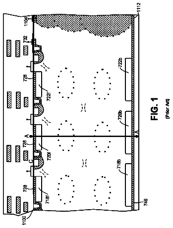
FIG. 1 is a schematic sectional view of a main portion of a solid-state imaging device according to a first embodiment of the invention;
FIG. 2 is a sectional view showing a state of light entering an opening of a light-shielding film;
FIG. 3 is a representation of the equation for determining the shape of the reverse tapered opening;
FIGS. 4A to 4C are schematic sectional views of exemplary structures of the reverse tapered opening;
FIGS. 5A to 5C are representations of a manufacturing method of a solid-state imaging device according to a first embodiment of the present invention;
FIGS. 6D and 6E are representations of the manufacturing method of the solid-state imaging device according to the first embodiment;
FIGS. 7A to 7C are representations of another manufacturing method of the solid-state imaging device according to the first embodiment;
FIG. 8 is a representation of an alternative step forming an antireflection layer;
FIG. 9 is a schematic sectional view of a main portion of a solid-state imaging device according to a second embodiment of the invention;
FIGS. 10A and 10B are representations of a manufacturing method of the solid-state imaging device according to the second embodiment;
FIGS. 11C and 11D are representations of the manufacturing method of the solid-state imaging device according to the second embodiment;
FIG. 12 is a schematic sectional view of a main portion of a solid-state imaging device according to a third embodiment of the invention;
FIG. 13 is a schematic sectional view of a main portion of a solid-state imaging device according to a fourth embodiment of the invention;
FIG. 14 is a schematic sectional view of a main portion of a solid-state imaging device according to a fifth embodiment of the invention; and
FIG. 15 is a schematic block diagram of an electronic apparatus according to a sixth embodiment of the invention.
Description of the preferred embodiments
Embodiments of the invention will now be described. The description will be made in the following order:
1. First Embodiment (structure and manufacturing method of solid-state imaging device)
2. Second Embodiment (Structure and manufacturing method of solid-state imaging device)
3. Third Embodiment (structure of solid-state imaging device)
4. Fourth Embodiment (structure of solid-state imaging device)
5. Fifth Embodiment (structure of solid-state imaging device)
6. Sixth Embodiment (structure of solid-state imaging device)
7. Seventh Embodiment (structure of electronic apparatus)
8. Eighth Embodiment (structure of camera module)
1. First Embodiment
Structure of Solid-State Imaging Device
The solid-state imaging device according to a first embodiment is a CCD image sensor. A CCD image sensor typically includes a plurality of photoelectric conversion portions acting as light-receiving portions, vertical transfer register portions having a CCD structure, arranged corresponding to each line of the photoelectric conversion portions, horizontal transfer register portions having a CCD structure, and an output portion.
FIG. 1 shows a solid-state imaging device according to the first embodiment of the invention, which is a CCD image sensor. FIG. 1 is a schematic sectional view showing one of a plurality of pixels arranged in a two-dimensional array (in a matrix manner) in an imaging region.
The solid-state imaging device 1 of the first embodiment includes second conductive semiconductor well regions 3 formed in a first conductive semiconductor substrate 2, and photoelectric conversion portions 4 acting as light-receiving portions in the respective semiconductor well regions 3. The photoelectric conversion portion 4 includes a first conductive semiconductor region 5 in which photoelectric conversion is performed and charges are stored, and a highly doped second conductive semiconductor region 6 reducing the dark current at the surface of the first conductive semiconductor region 5. The photoelectric conversion portion 4 is a so-called photodiode.
In the present embodiment, the first conductive type is the n type, and the second conductive type is the p type. Hence, a p-type semiconductor well region 3 is formed in an n-type semiconductor substrate 2, and the photoelectric conversion portion 4 is formed in the p-type semiconductor well region 3, in the present embodiment.
The p-type semiconductor well region 3 is also provided with an n-type embedded channel region 7 close to the photoelectric conversion portion 4 and a p-type channel stop region 8 surrounding the photoelectric conversion portion 4. The embedded channel region 7 receives charges from the photoelectric conversion portion 4, as will be described below, and transfers the charges in the vertical direction, thus functioning as a charge-receiving region. A second p-type semiconductor well region 9 is formed immediately under the embedded channel region 7. The region between the photoelectric conversion portion 4 and the embedded channel region 7 acts as a charge read-out region 11 that reads out the charge of the photoelectric conversion portion 4 to the embedded channel region 7. A vertical transfer gate electrode 13 is disposed so as to cover the read-out region 11, the embedded channel region 7 and the channel stop region 8 on the surface of the semiconductor substrate 2 with a gate insulating film 12 therebetween. A plurality of the vertical transfer gate electrodes 13 are arranged along the charge transfer direction.
The embedded channel region 7 and the vertical transfer gate electrodes 13 over the embedded channel region 7 define a vertical transfer register portion 15 having a CCD structure, and the read-out region 11 and a read-out gate electrode over the read-out region 11 define a read-out gate portion 16. The read-out gate electrode doubles as the vertical transfer gate electrode 13. A unit pixel includes one photoelectric conversion portion 4 and the corresponding vertical transfer register portion 15. A plurality of unit pixels are regularly arranged in a two-dimensional array (in a matrix manner) so as to define an imaging region.
In the present embodiment, a light-shielding film 21 acting as a light control film, having a reverse tapered opening 19 is formed on an insulating interlayer 18 formed over the entire surface to cover the vertical transfer gate electrodes 13. The insulating interlayer 18 also acts as an antireflection layer over the photoelectric conversion portion 4, and is made of, for example, silicon nitride. The light-shielding film 21 is formed in such a manner that the opening 19 is located corresponding to the photoelectric conversion portion 4; hence, the light-shielding film 21 is formed over the entire surface except the region overlying the photoelectric conversion portion 4. The light-shielding film 21 juts into the region overlying the photoelectric conversion portion 4, and accordingly, the lower end of the opening 19 has a smaller area than the photoelectric conversion portion 4.
An insulating interlayer 22 is formed over the entire surface of the light-shielding film 21 including the inside of the opening 19, and an in-layer lens 23 is formed on the insulating interlayer 22 in a region corresponding to the photoelectric conversion portion 4. The in-layer lens 23 is made of an insulating material having a different refractive index from the material of a surface protective layer 24 covering the in-layer lens 23. Furthermore, after forming a planarizing layer 25, a color filter 26 and an on-chip microlens 27 are provided.
In the solid-state imaging device 1 of the present embodiment, incoming light passes through the on-chip microlens 27, the color filter 26, the planarizing layer 25 and the surface protective layer 24. The light further passes through the in-layer lens 23 to be condensed and enters the photoelectric conversion portion 4 through the opening 19 of the light-shielding film 21. The light is converted in the photoelectric conversion portion 4 to electricity to generate charges or electrons used as signal charges, and these electrons are stored in the semiconductor region 5. When a read-out gate pulse is applied to the read-out gate electrode doubling as the vertical transfer gate electrode 13, the charges in the semiconductor region 5 is read out to the vertical transfer register portion 15. The charges in the vertical transfer register portion 15 is transferred in the vertical direction to a horizontal transfer register portion (not shown) having a CCD structure by a pulsed vertical driving voltage applied to the vertical transfer gate electrode 13. The charges in the horizontal transfer register are transferred in the horizontal direction by horizontal driving pulses, and the charges are converted to a voltage in an output portion and outputted as a pixel signal.
If light entering through the opening 19 of the light-shielding film 21 diffuses to regions other than the photoelectric conversion portion and enters the vertical transfer register portion to be converted to an electrical signal, this signal acts as noise relative to the charges stored in the semiconductor region 5. In other words, smear components produced from the light diffused to regions other than the photoelectric conversion portion act as noise. It is therefore important to prevent light from entering regions other than the photoelectric conversion portion, in terms of improving the characteristics of the CCD image sensor.
The first embodiment features the light-shielding film 21 having the reverse tapered opening 19. FIG. 2 shows a case in which light enters the opening 19 of the light-shielding film 21. As shown in FIG. 2, a difference (optical path difference) between the optical path a of light La propagating in straight lines in the opening 19 and an optical path b of diffracted light Lb along the tapered face of the opening 19 produces a phase difference in a region c including a region other than the photoelectric conversion portion. The intensity of the diffracted light Lb is reduced in this region c. Consequently, light entering the photoelectric conversion portion can be prevented from diffusing in the horizontal direction.
The reverse tapered shape of the opening 19 can be determined by using the following equation: 1/2.lamda.(n-1)= {square root over ((d.sup.2+(y-x)/2).sup.2)}-d
This equation represents the conditions where light L having entered the reverse tapered opening 19 of the light-shielding film 21 shown in FIG. 3 is diffracted at the upper edge of the opening 19 (x face) and the phase of the light is reversed precisely at the lower edge (y faces). In FIG. 3, the thickness of the light-shielding film, or the height of the reverse tapered portion, is represented by d (nm); the upper diameter of the opening 19 is represented by x (nm); the lower diameter of the opening 19 is represented by y (nm); the refractive index of the material defining the opening 19, that is, the refractive index of the insulating interlayer 22, is represented by n; and the wavelength of incoming light L is represented by .lamda. (nm).
The light-shielding film 21, which preferably has a sufficient shielding property against light used in the solid-state imaging device, is made of tungsten (W), aluminum (Al), tantalum (Ta), ruthenium (Ru) or the like.
The thickness of the light-shielding film 21 is set so that light diffracted through the opening 19 can propagate within the opening 19 as is. The thickness of the light-shielding film 21 also depends on the desired light-shielding property. For example, a tungsten (W) light-shielding film preferably has a thickness of about 100 to 300 nm. A thickness of less than 100 nm does not provide a sufficient light-shielding property. In contrast, a thickness of larger than 300 nm forms a large step height, and accordingly, layers overlying the light-shielding film 21 are not planarized.
When light having a wavelength of 550 nm enters the opening 19 of the light-shielding film 21 having a thickness d of 200 nm through the insulating interlayer 22 having a refractive index of 1.45, the reverse taper angle .theta. at which diffraction can be minimized is 48.degree. from the above equation.
Since the incident angle distribution is varied depending on the shapes of the on-chip microlens 27 and the in-layer lens 23, the most suitable shape obtained from the above equation can produce an effective effect when the reverse taper angle .theta. of the shape has a tolerance within .+-.10.degree. (.theta.>0.degree.).
Preferably, the light-shielding film 21 has a multilayer structure including at least two layers having different etching properties in view of the process for forming the light-shielding film 21 as described below. In this instance, the light-shielding film 21 preferably has a reverse tapered section or a section having a plurality of steps corresponding to the layers of the light-shielding film 21 (multi-step shape). For a section having a multi-step shape, the reverse tapered angle .theta. obtained from the above equation is defined by the angle formed with the base of the opening 19 and the inclined line connecting the uppermost and lowermost edges of the opening 19 in the light-shielding film 21.
The reverse tapered shape of the opening 19 in the light-shielding film 21 is effective in reducing the intensity of diffracted light having long wavelengths. In the present embodiment, openings 19 having the same reverse tapered shape are formed for red, green and blue pixels, that is, openings 19 having a reverse tapered shape for wavelengths of red light. In this instance, the opening 19 can be formed according to wavelengths of red light by controlling the reverse taper angle .theta. without varying the thickness of the light-shielding film 21.
FIGS. 4A to 4C show examples of the section of the light-shielding film 21 having a reverse tapered opening. The opening shown in FIG. 4A has a trapezoidal section. The opening shown in FIG. 4B has a section having concave sides and a reverse taper angle .theta. between the base of the opening and the inclined line connecting the upper and lower edges of the opening. The opening shown in FIG. 4C is defined by a plurality of layers 20 and has a multi-step section having a reverse taper angle .theta. between the base of the opening and the inclined line connecting the upper and lower edges of the opening. The opening having the section shown in FIG. 4C can be formed as below. A plurality of layers having different etching properties are formed. More specifically, the layers are formed in decreasing order of etching rate, and then the layers are subjected to dry etching or wet etching so as to form an opening having steps whose diameter increases downward. For example, for a film including a W lower layer and an Al upper layer, a desired shape can be formed by etching the Al layer with chlorine gas, and subsequently etching the W layer with a fluorine-based gas.
In the CCD image sensor 1 of the first embodiment, the light-shielding film 21 has an opening 19 having a reverse tapered shape. The reverse tapered shape can ensure that incoming light propagates to the photoelectric conversion portion 4, and hence it can prevent diffracted light from diffusing to regions other than the photoelectric conversion portion 4. Accordingly, the sensitivity of the CCD image sensor can be enhanced. In addition, diffracted light is prevented from entering the vertical transfer register portion, and thus, smears can be reduced. The present embodiment produces a marked effect particularly in solid-state imaging devices including a large number of miniaturized pixels. Since such a solid state imaging device can reduce the intensity of diffracted light diffusing to regions other than the photoelectric conversion portion, the sensitivity can be enhanced and smears can be reduced.
Method for Manufacturing Solid-State Imaging Device
FIGS. 5A to 6D show an exemplary method for manufacturing the solid-state imaging device 1, or CCD image sensor, according to the first embodiment. First, as shown in FIG. 5A, a p-type semiconductor well region 3 is formed in an n-type silicon semiconductor substrate 2. The p-type semiconductor well region 3 is subjected to ion implantation of an n-type impurity and a p-type impurity to form a photoelectric conversion portion (photodiode) 4 including an n-type semiconductor region 5 and a p-type semiconductor region 6. The photoelectric conversion portion acts as a light-receiving portion. The p-type semiconductor well region 3 is provided therein with an n-type embedded channel region 7, a p-type channel stop region 8, and a second p-type semiconductor well region 9 immediately under the embedded channel region 7. A silicon oxide gate insulating film 12 is formed so as to have a thickness of about 50 nm over the surface of the semiconductor substrate 2 by thermal oxidation.
Subsequently, a polysilicon layer is formed on the gate insulating film 12 by chemical vapor deposition (CVD), and a tungsten silicide (WSi) layer is further formed by, for example, sputtering. The WSi layer and the polysilicon layer are selectively etched through a positive resist mask formed by lithography on the region where electrodes are to be formed, and thus a vertical transfer gate electrode 13 is formed as shown in FIG. 5B. The vertical transfer gate electrode 13, part of which acts as a read-out electrode, is disposed over the area including the read-out region 11, the embedded channel region 7 and the p-type channel stop region 8.
Subsequently, as shown in FIG. 5C, a silicon oxide layer (not shown) is formed over the entire surface to cover the vertical transfer gate electrodes 13 by thermal oxidation and CVD, and then an antireflection layer 18 is formed so as to cover the photoelectric conversion portion 4 by vacuum CVD. The antireflection layer 18 may be, for example, a silicon nitride (SiN) film or a silicon oxynitride (SiON) film. The antireflection layer 18 is formed over the entire surface covering the photoelectric conversion portion 4. Furthermore, a silicon oxide layer (not shown) is formed over the entire surface of the antireflection layer 18 by CVD. Then, the material of the light-shielding film, such as tungsten (W), is deposited by sputtering and further deposited continuously by CVD to form a material layer having a sufficient thickness to act as a light-shielding film over the entire surface. The tungsten layer formed by sputtering enhances the adhesion to the underlayer.
Subsequently, a positive resist mask is formed on the material layer of the light-shielding film by lithography. The material layer is selectively etched through the resist mask so that the portion of the material layer overlying the photoelectric conversion portion 4 is removed to form a light-shielding film 21 acting as a light control film having a reverse tapered opening 19 in the region corresponding to the photoelectric conversion portion 4, as shown in FIG. 6D.
The reverse tapered opening 19 can be formed by, for example, an etching process as shown in FIGS. 7A to 7C. Specifically, after forming the material layer (first material layer) for the light-shielding film 21, another material layer or a second material layer 31 having a different etching property from the first material layer is formed on the first material layer, as shown in FIG. 7A. The second material layer 31 may be formed of silicon oxynitride.
Then, anisotropic dry etching is performed through a resist mask so that the entire thickness of the second material layer 31 and a depth of the first material layer 21A are selectively removed, as shown in FIG. 7B.
Subsequently, the rest of the depth of the first material layer is removed by selective isotropic etching through the resist mask, as shown in FIG. 7C. The isotropic etching may be performed by a dry process or a wet process. The reverse tapered opening 19 thus can be formed by selectively etching an additionally formed second material layer 31.
Although the antireflection layer 18 is formed before forming the light-shielding film 21 in an embodiment, as shown in FIG. 6D, it may be formed after forming the light-shielding film 21, as shown in FIG. 8.
Subsequently, as shown in FIG. 6E, an insulating interlayer 22 is formed of, for example, BPSG (boron phosphosilicate glass) by CVD, followed by reflowing at about 800.degree. C. In addition, an in-layer lens 23 is formed of, for example, silicon nitride on the insulating interlayer 22 by an existing technique. Then, a surface protective layer 24, a planarizing layer 25, a color filter 26 and an on-chip microlens 27 (each not shown) are formed in that order to complete a desired solid-state imaging device 1.
In the method for manufacturing a solid-state imaging device of the present embodiment, a light-shielding film 21 having a reverse tapered opening 19 can be formed. Since the opening can prevent diffracted light from entering the vertical register portion, the CCD image sensor 1 can reduce smears and exhibits enhanced sensitivity.
2. Second Embodiment
Structure of Solid-State Imaging Device
The solid-state imaging device according to a second embodiment is a CMOS image sensor. A CMOS image sensor typically includes an imaging region and a peripheral circuit region. The imaging region includes a plurality of pixels, each including a photoelectric conversion portion acting as a light-receiving portion. The unit pixel may include one photoelectric conversion portion and a plurality of pixel transistors (MOS transistors). Alternatively, a pixel-sharing structure may be applied in which a plurality of photoelectric conversion portions share pixel transistors other than the transfer transistor and the floating diffusion portion. The pixel transistors may include four transistors of a transfer transistor, a reset transistor, an amplification transistor and a selection transistor, or three transistors other than the selection transistor.
FIG. 9 shows a solid-state imaging device according to the second embodiment of the invention, which is a CMOS image sensor. FIG. 9 is a schematic sectional view showing one of a plurality of pixels arranged in a two-dimensional array (in a matrix manner) in the imaging region.
The solid-state imaging device 41 of the second embodiment has pixels, each disposed in a semiconductor well region 43 formed in a first conductive silicon semiconductor substrate 42. The pixel includes a photoelectric conversion portion 44 acting as a light-receiving portion and a plurality of transistors. A plurality of unit pixels is regularly arranged in a two-dimensional array in, for example, a matrix manner to define an imaging region. In the present embodiment, the p-type semiconductor well region 43 is formed in an n-type semiconductor substrate 42, and the plurality of pixels is formed in the semiconductor well region 43 to define an imaging region.
The photoelectric conversion portion 44 includes an n-type semiconductor region 45 performing photoelectric conversion and storing charges, and a highly doped p-type semiconductor region 46 reducing the dark current at the surface of the n-type semiconductor region 45. The photoelectric conversion portion 44 is defined by a so-called photodiode. In the present embodiment, the pixel transistors include four transistors of a transfer transistor Tr1, a reset transistor, an amplification transistor, and a selection transistor (latter three not shown). The transfer transistor Tr1 is disposed close to the photoelectric conversion portion 44.
Element isolation regions 48 are formed on the p-type semiconductor well region 43 to separate the pixels from each other and divide the pixel. The element isolation region 48 may be defined by a shallow trench isolation (STI) structure, an oxide film formed by local oxidation of silicon (LOCOS oxide film), a structure in which an insulating film is formed on a highly doped p-type semiconductor region, or a highly doped p-type semiconductor region. In the present embodiment, the element isolation region 48 is made of a LOCOS oxide film. P-type semiconductor regions 49 more highly doped than the p-type semiconductor well region 43 are formed in the p-type semiconductor well region 43 so as to surround the element isolation regions 48.
The transfer transistor Tr1 includes the photoelectric conversion portion 44 as a source, the floating diffusion portion 51 of an n-type semiconductor region as a drain, and a transfer gate electrode 53 on a gate insulating film 52. The floating diffusion portion 51 is a region to which charges are transferred from the photoelectric conversion portion 44, and thus functions as a charge-receiving region.
Then, an optical waveguide 55 is provided over the photoelectric conversion portion 44, in the present embodiment. The optical waveguide 55 is formed on an antireflection layer 54 that is formed over the entire surface to cover the transfer gate electrode 53 and the gate electrodes of the other pixel transistors. Also, the optical waveguide 55 is formed in a multilayer wiring layer 64 including a plurality of layers of wirings 63 disposed in a second insulating interlayer 58 (described later). The wirings 63 are formed in the entire region of the insulating interlayer 58 except the region corresponding to the photoelectric conversion portion 44 and the optical waveguide 55. At the lower end of the optical waveguide 55, a first insulating interlayer 56 is formed as a first material layer of a light control film having a reverse tapered opening 57.
More specifically, the optical waveguide 55 is formed of an insulating material 61 filling the reverse tapered opening 57 in the first insulating interlayer 56 and a forward tapered opening 59 formed in the second insulating interlayer 58. The insulating material 61 has a higher refractive index than the second insulating interlayer 58 and the first insulating interlayer 56. The second insulating interlayer 58 corresponds to a second material layer. The opening 57 is formed in the first insulating interlayer 56 so that the lower end of the opening 57 has a smaller area than the photoelectric conversion portion 44.
In the optical waveguide 55, the interface between the second insulating interlayer 58 and the insulating material 61 filling the opening 59 acts as a total reflection surface at which light having entered the optical waveguide 55 is totally reflected. The reverse tapered shape of the opening 57 of the first insulating interlayer 56, that is, the shape of the lower end acting as a light control film of the optical waveguide 55 satisfies the requirements for reducing the intensity of diffracted light diffusing to regions other than the photoelectric conversion portion 44 and can be obtained from the above-described equation. The other structural properties of the first insulating interlayer having a reverse tapered opening are the same as those of the light-shielding film 21 described in the first embodiment, and the same description will be omitted.
A color filter 66 and an on-chip microlens 67 are formed on the second insulating interlayer 58 including the optical waveguide 55 with a surface protective layer and a planarizing layer (each not shown) therebetween.
The description continues in the full USPTO document.
 Lapsed, fee not paid23 drawings