 Lapsed, fee not paid1 drawing
Cameras, Displays & Optics · US 8,545,984 B2
Photochromic compounds and compositions
Described herein are compounds generally comprising an indeno[2',3':3,4]naptho[1,2-b]pyran structure.
US 8,546,049 B2 · Assignee: Sharp Kabushiki Kaisha · Inventors: Kihara; Akiko et al.
Sheet 1 of 2 from the published document. All sheets in the USPTO PDF
An electrophotographic photoconductor comprising a charge generation layer containing a charge generation material and a charge transfer layer containing a charge transfer material laminating in this order on a conductive support with an undercoat layer interposed between the charge generation layer and the conductive support, or comprising a monolayer type photosensitive layer containing a charge generation material and a charge transport material being formed on a conductive support with an undercoat layer interposed between the monolayer type photosensitive layer and the conductive support, wherein the charge transport layer or the monolayer type photosensitive layer contains, as a charge transfer material, a bisamine compound represented by the following general formula (I): ##STR00001##
In recent years, organic photoconductive materials are pit on wide-ranging studies and researches. The organic photoconductive materials not only are used for electrophotographic photoconductors (hereinafter, also referred to as simply "photoconductor"), but also have become used in applications of electrostatic recording devices, sensor materials or organic electro luminescent (abbreviation: EL) devices. Further, the electrophotographic photoconductor using the organic photoconductive material is used not only for the copier field, but also for the fields of printing plates, slide films and micro films, where a photographic technology is heretofore used, and is also applied to high-speed printers using laser, a light emitting diode (abbreviation: LED) or a cathode ray tube (abbreviation: CRT) as a light source. Therefore, requirements of the organic photoconductive material and the elec
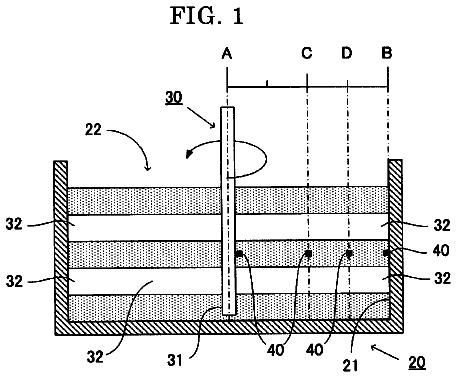
1 of 2 drawing sheets so far from the published document, cropped to the drawing. Every sheet is in the USPTO PDF.
What the patent claimed, word for word. All of it is now free to use.
This application is related to Japanese Patent Application No. 2010-284622 filed on 21 Dec. 2010, whose priority is claimed under 35 USC .sctn.119, and the disclosure of which is incorporated by reference in its entirety.
The present invention relates to an electrophotographic photoconductor in which a bisamine compound having a specific bisbutadiene structure is included in a photosensitive layer formed on a conductive support, and an image forming apparatus.
In recent years, organic photoconductive materials are pit on wide-ranging studies and researches. The organic photoconductive materials not only are used for electrophotographic photoconductors (hereinafter, also referred to as simply "photoconductor"), but also have become used in applications of electrostatic recording devices, sensor materials or organic electro luminescent (abbreviation: EL) devices. Further, the electrophotographic photoconductor using the organic photoconductive material is used not only for the copier field, but also for the fields of printing plates, slide films and micro films, where a photographic technology is heretofore used, and is also applied to high-speed printers using laser, a light emitting diode (abbreviation: LED) or a cathode ray tube (abbreviation: CRT) as a light source. Therefore, requirements of the organic photoconductive material and the electrophotographic photoconductor using the organic photoconductive material are becoming highly advanced and widely spread.
Hitherto, as the electrophotographic photoconductor, widely used are inorganic photoconductors which are provided with a photosensitive layer containing, as its major component, an inorganic photoconductive material such as selen, zinc oxide or cadmium. The inorganic photoconductor has fundamental characteristics required as photoconductors to some extent. However, the inorganic photoconductor has a drawback such that it has a difficulty in forming a film of the photosensitive layer, is deteriorated in plasticity and has high production cost. Also, the inorganic photoconductive materials are highly toxic in general and are therefore largely limited in its production and handling.
On the other hand, an organic photoconductor using the organic photoconductive material has advantages that a film formation property of the photoconductive layer is good, flexibility is high, and the photoconductor is lightweight and highly transparent, and a photoconductor, which exhibits a good sensitivity for a wide-ranging wavelength region by an appropriate sensitizing method, can be easily designed, and therefore the organic photoconductor is being developed as mainstreams of the electrophotographic photoconductor. The organic photoconductor had defects in a sensitivity and a durability early, but these defects are outstandingly improved by a development of a function separated electrophotographic photoconductor in which a charge generation function and a charge transport function are shared on separate materials respectively. The function separated electrophotographic photoconductor also has an advantage that each of a charge generation material bearing the charge generation function and a charge transport material bearing the charge transport function can be selected from wide-ranging materials and a electrophotographic photoconductor having any characteristic can be relatively easily prepared.
As the charge generation material to be used in these function separation type photoconductors, studies have been made as to various materials such as a phthalocyanine pigment, a squalilium dye, an azo pigment, a perylene pigment, a polycyclic quinone pigment, a cyanine dye, a squaric acid dye and a pyrylium salt-based dye, and a variety of materials having a high light fastness and a high charge generation ability have been proposed.
On the other hand, as the charge transport material, there are known various compounds such as pyrazoline compounds (e.g., see Japanese Examined Patent Publication No. 52-4188), hydrazone compounds (e.g., see Japanese Unexamined Patent Publication No. 54-150128, Japanese Examined Patent Publication No. 55-42380 and Japanese Unexamined Patent Publication No. 55-52063), triphenylamine compounds (e.g., see Japanese Examined Patent Publication No. 58-32372 and Japanese Unexamined Patent Publication No. 2-190862) and stilbene compounds (e.g., see Japanese Unexamined Patent Publication No. 54-151955 and Japanese Unexamined Patent Publication No. 58-198043). In recent years, pyrene derivatives, naphthalene derivatives and terphenyl derivatives (e.g., see Japanese Unexamined Patent Publication No. 7-48324), which have condensed polycyclic hydrocarbons as a central mother nucleus, are developed.
The following items of the charge transport material are required:
to be stable against light and heat;
to be stable against ozone, nitrogen oxide (NOx) and nitric acid respectively generated by corona discharge in charging a surface of the photoconductor;
to have a high charge transport ability;
to have a high compatibility with an organic solvent or agent; and
to be easily and economically produced.
However, the above-mentioned charge transport materials satisfy a part of these requirements but do not satisfy all of the requirements at a high level.
Further, among these requirements, it is particularly required to have a high charge transport ability. For example, when a charge transport layer formed by dispersing the charge transport material together with a binder resin is a surface layer of the photoconductor, the charge transport material requires the high charge transport ability in order to secure a sufficient photoresponsivity. When the photoconductor is disposed in a copier or a laser beam printer for use, the surface layer of the photoconductor is necessarily partly shaved off by a contact member such as a cleaning blade or a charge roller. In order to enhance a durability of the copier or the laser beam printer, a surface layer resistant to these contact members, that is, a surface layer having a high printing durability, which is less shaved by these contact member, is required. Thus, if a content of the binder resin in the charge transport layer, the surface layer, is increased in order to strengthen the surface layer and improve the durability, the photoresponsivity is deteriorated. A reason for this is that since the charge transport ability of the charge transport material is low, the charge transport material in the charge transport layer is diluted as the content of the binder resin increases, and therefore the charge transport ability of the charge transport layer is further lowered to deteriorate the photoresponsivity. When the photoresponsivity is poor, a residual potential is increased and the photoconductor is used repeatedly with a surface potential of the photoconductor not adequately decreased, and therefore a surface charge of a part to be eliminated by exposure is not adequately eliminated and this causes troubles such as reduction in image quality at an early stage. Accordingly, in order to secure the sufficient photoresponsivity, the high charge transport ability of the charge transport material is required. Further, a material, which can secure an adequate printing durability while maintaining the high charge transport ability without increasing a ratio of the binder resin by firmly bonding to the binder resin, is required.
Moreover, recently, downsizing and speeding up of electrophotography apparatuses such as a digital copier and a printer are advanced, an increase in sensitivity according to speeding up is required as the photoconductor characteristics and a higher charge transport ability of the charge transport material is required. In a high-speed process, since a time between exposure and developing is short, a photoconductor having a high photoresponsivity is necessary. As described above, since the photoresponsivity depends on the charge transport ability of the charge transport material, also from this point of view, the charge transport material having a higher charge transport ability is required.
With respect to a charge transport material satisfying such requirements, as a compound having a higher charge mobility than the aforementioned charge transport material, a trial of a compound, in which a charge mobility of the charge transport material is increased by having a bisbutadiene structure in a molecule to expand a conjugated system in the molecule, is made (e.g., Japanese Unexamined Patent Publication No. 2002-275135 and Japanese Unexamined Patent Publication No. 9-244278).
However, even though various organic compounds are developed as the charge transport material like these, there is no organic compound overcoming all of the following problems such as:
1) a compatibility with a binding agent is low;
2) crystal is easily precipitated;
3) changes in sensitivity occur in the case of repetitive use;
4) a charging ability and a repetitive characteristic are low; and
5) a residual potential characteristic is poor.
It is a current status that an organic compound, which satisfies essential properties required as the photoconductor previously described, a mechanical strength and a high durability, is not yet adequately attained.
It is an object of the present invention to provide an electrophotographic photoconductor having a high sensitivity and a high durability, and an image forming apparatus.
The inventors of the present invention have made studies concerning photoconductive materials having a high sensitivity, a high durability and a high wear resistance of the above objects, and as a result, found that a bisamine compound having a bisbutadiene structure represented by the following general formula (I) is useful, to complete the present invention.
Specifically, in accordance with the present invention, there is provided an electrophotographic photoconductor including a charge generation layer containing a charge generation material and a charge transfer layer containing a charge transfer material laminating in this order on a conductive support with an undercoat layer interposed between the charge generation layer and the conductive support, or including a monolayer type photosensitive layer containing a charge generation material and a charge transport material being formed on a conductive support with an undercoat layer interposed between the monolayer type photosensitive layer and the conductive support, wherein the charge transport layer or the monolayer type photosensitive layer contains, as a charge transfer material, a bisamine compound represented by the following general formula (I):
##STR00002## wherein Ar.sub.1s each represent an aryl, heteroaryl, aralkyl or heteroaralkyl group which may have a substituent, Ar.sub.2s each represent and arylene or heterorylene group which may have a substituent, Ar.sub.3s and Ar.sub.4s may be the same or different and each represent a hydrogen atom or a alkyl or aryl group which may have a substituent, R.sub.1 and R.sub.2 may be the same or different and each represents a C.sub.1 to C.sub.4 alkyl, C.sub.1 to C.sub.4 alkoxy or C.sub.1 to C.sub.4 dialkylamino group which may have a halogen atom or a substituent, m is an integer of 0 to 4, and n is an integer of 1 to 4.
Also, in accordance with the present invention, there is provided the electrophotographic photoconductor, wherein the charge generation material contains oxotitanium phthalocyanine in which a Bragg angle (2.theta..+-.0.2 degree) in a Cu--K.alpha. characteristic X-ray diffraction (wavelength: 1.54 angstroms) has a clear diffraction peak at least at 27.2 degree.
Also, in accordance with the present invention, there is provided the electrophotographic photoconductor, wherein the charge transport layer further contains a binder resin, and in the charge transport layer, a ratio A/B (by mass) of the charge transport material (A) to the binder resin (B) is 10/12 or more and 10/30 or less.
Moreover, in accordance with the present invention, there is provided an image forming apparatus including the electrophotographic photoconductor, a charging means for charging the electrophotographic photoconductor, an exposure means for exposing the charged electrophotographic photoconductor with light to form an electrostatic latent image, a developing means for developing the electrostatic latent image to form a toner image, a transfer means for transferring the formed toner image to a medium, a cleaning means for removing and recovering a toner remaining on the photoconductor, a fixing means for fixing the toner image transferred to a medium to the medium and a charge-removing means for removing a surface charge remaining in the photoconductor.
When the bisamine compound represented by the general formula (I) according to the present invention is used, since the photoconductor has an excellent mechanical durability, a durability of the photoconductor can be improved without increasing a content of the binder resin at the expense of an electric characteristic as distinct from a case of using a common charge transport material.
Accordingly, it becomes possible to lengthen a lifetime of the electrophotographic photoconductor. Further, since the bisamine compound represented by the following compounds 1 to 5 can be easily produced, a productivity of the electrophotographic photoconductor can be improved.
Also, in accordance with the present invention, it is possible to provide a photoconductor which has a high charge characteristic and hardly causes a reduction in sensitivity also in a case of repetitive use. Further, it becomes possible to provide an image which is stable for a long period since a wear resistance of a surface of the photoconductor is excellent.
In accordance with the present invention, by containing the bisamine compound as the charge transport material, it is possible to provide an electrophotographic photoconductor having a high printing durability capable of providing an image which has a high sensitivity and a high responsivity and is stable for a long period. Also, in accordance with the present invention, it is possible to provide an electrophotographic photoconductor which has advantages of an organic-based photoconductor such that the organic-based photoconductor is highly transparent and lightweight and has an excellent film forming property and an ability to be positively and negatively charged and is easy to be produced, and has an excellent characteristic of hardly causing a reduction in photosensitivity even in repetitive use, and an image forming apparatus including the photoconductor.
FIG. 1 is a schematic cross-sectional view showing a structure of an electrophotographic photoconductor of an example of an embodiment of the present invention;
FIG. 2 is a schematic cross-sectional view showing a structure of an electrophotographic photoconductor of another example of an embodiment of the present invention;
FIG. 3 is a schematic cross-sectional view showing a structure of an electrophotographic photoconductor of further example of an embodiment of the present invention; and
FIG. 4 is an arrangement side view schematically showing a structure of an image forming apparatus including a electrophotographic photoconductor according to the present invention.
The term "C.sub.1 to C.sub.4 alkyl group" used in the present invention means a straight or branched chain alkyl group having 1 to 4 carbon atoms.
Specific examples of the "C1 to C4 alkyl group" include methyl, ethyl, n-propyl, isopropyl, n-butyl and t-butyl group.
The term "C.sub.1 to C.sub.4 alkoxy group" used in the present invention means a straight or branched chain alkoxy group having 1 to 4 carbon atoms.
Specific examples of the "C.sub.1 to C.sub.4 alkoxy group" include methoxy, ethoxy, n-propoxy, isopropoxy, n-butoxy and t-butoxy group.
Further, the term "halogen atom" used in the present invention means fluorine, chlorine, bromine or iodine atom.
An electrophotographic photoconductor according to the present invention includes a charge generation layer containing a charge generation material and a charge transfer layer containing a charge transfer material laminating in this order on a conductive support with an undercoat layer interposed between the charge generation layer and the conductive support, or includes a monolayer type photosensitive layer containing a charge generation material and a charge transport material being formed on a conductive support with an undercoat layer interposed between the monolayer type photosensitive layer and the conductive support, wherein the charge transport layer or the monolayer type photosensitive layer contains, as a charge transfer material, a bisamine compound represented by the following general formula (I):
##STR00003## wherein, Ar.sub.1s each represent an aryl, heteroaryl, aralkyl or heteroaralkyl group which may have a substituent, Ar.sub.2s each represent an arylene or heteroarylene group which may have a substituent, Ar.sub.3s and Ar.sub.4s may be the same or different and each represent a hydrogen atom or an alkyl or aryl group which may have a substituent, R.sub.1 and R.sub.2 may be the same or different and each represents a C.sub.1 to C.sub.4 alkyl, C.sub.1 to C.sub.4 alkoxy or C.sub.1 to C.sub.4 dialkylamino group which may have a halogen atom or a substituent, m is an integer of 0 to 4, and n is an integer of 1 to 4.
In the general formula (I), Ar.sub.1s each represent an aryl, heteroaryl, aralkyl or heteroaralkyl group which may be substituted with one or more halogen atoms, or one or more straight or branched chain C.sub.1 to C.sub.4 alkyl or C.sub.1 to C.sub.4 alkoxy groups,
Ar.sub.1s each are an arylene or heteroarylene group which may be substituted with one more substituents, whose substituent is halogen atom, or one or more straight or branched chain C.sub.1 to C.sub.4 alkyl or C.sub.1 to C.sub.4 alkoxy groups,
R.sub.1 and R.sub.2 may be the same or different and each represents a C.sub.1 to C.sub.3 alkyl, C.sub.1 to C.sub.3 alkoxy or C.sub.1 to C.sub.3 dialkylamino group which may be substituted with one or more halogen atoms, or one or more straight or branched chain C.sub.1 to C.sub.4 alkyl or C.sub.1 to C.sub.4 alkoxy groups, and m is an integer of 0 to 4 and n is an integer of 1 to 4.
Specifically, in the general formula (I), Ar.sub.1s each represent a phenyl or naphthyl group which may be substituted with one or more halogen atoms, or one or more straight or branched chain C.sub.1 to C.sub.4 alkyl or C.sub.1 to C.sub.4 alkoxy groups,
Ar.sub.2s each are an arylene group selected from the group consisting of phenylene, naphthylene and biphenylene which may be substituted with one or more halogen atoms, or one or more straight or branched chain C.sub.1 to C.sub.4 alkyl or C.sub.1 to C.sub.4 alkoxy groups; or each are a heteroallylene group selected from the group consisting of furylene, thienylene and thiazolylene which may be substituted with one or more halogen atoms, or one or more straight or branched chain C.sub.1 to C.sub.4 alkyl or C.sub.1 to C.sub.4 alkoxy groups, Ar.sub.3s and Ar.sub.4s may be the same or different and each are a hydrogen atom, or a straight or branched chain C.sub.1 to C.sub.4 alkyl group which may be substituted with one or more substituents, whose substituent is halogen atom, or one or more straight or branched chain C.sub.1 to C.sub.4 alkyl or C.sub.1 to C.sub.4 alkoxy groups; or an aryl group selected from the group consisting of a phenyl, naphthyl and biphenyl group which may be substituted with one or more halogen atoms, or one or more straight or branched chain C.sub.1 to C.sub.4 alkyl or C.sub.1 to C.sub.4 alkoxy groups, R.sub.1 and R.sub.2 are respectively an alkyl group selected from the group consisting of a methyl, ethyl, n-propyl, isopropyl, n-butyl and t-butyl group which may be substituted with halogen atom, and m is an integer of 0 or 1 and n is an integer of 1 to 4.
More specifically, in the general formula (I), Ar.sub.1s each represent a phenyl or naphthyl group,
Ar.sub.2s each are a phenylene or naphthylene group which may be substituted with methyl, ethyl, methoxy or ethoxy group,
Ar.sub.3s and Ar.sub.4s may be the same or different and each are a hydrogen atom, or a phenyl or naphthyl group which may be substituted with one or more halogen atoms, or one or more straight or branched chain C.sub.1 to C.sub.4 alkyl or C.sub.1 to C.sub.4 alkoxy groups,
R.sub.1 and R.sub.2 are respectively an alkyl group selected from the group consisting of methyl, ethyl, n-propyl, isopropyl, n-butyl and t-butyl group which may be substituted with halogen atom, and
m is an integer of 0 or 1 and n is an integer of 1 to 4.
Furthermore specifically, in the general formula (I), Ar.sub.1s each represent a phenyl group,
Ar.sub.2s each are 1,4-phenylene, 2-methyl-1,4-phenylene, 3-methyl-1,4-phenylene or 1,4-naphthylene group,
Ar.sub.3s and Ar.sub.4s may be the same or different and each are hydrogen atom or phenyl group, and
m is 0 and n is an integer of 1 or 2.
Specific examples of each substituent in the bisamine compound represented by the general formula (I) of the present invention are shown in the following table, but the bisamine compound of the present invention is not limited thereto.
TABLE-US-00001 TABLE 1 Compound Ar.sub.1 N--Ar.sub.2 Ar.sub.3 Ar.sub.4 R.sub.1 R.sub.2 m n 1 ##STR00004## ##STR00005## ##STR00006## H (H) (H) 0 1 2 ##STR00007## ##STR00008## ##STR00009## H (H) (H) 0 1 3 ##STR00010## ##STR00011## ##STR00012## H (H) (H) 0 1 4 ##STR00013## ##STR00014## ##STR00015## H (H) (H) 0 1 5 ##STR00016## ##STR00017## ##STR00018## H (H) (H) 0 2
More specific bisamine compounds represented by the general formula (I) are compounds having the following structural formula.
TABLE-US-00002 TABLE 2 Compound Structural formula 1 ##STR00019## 2 ##STR00020## 3 ##STR00021## 4 ##STR00022## 5 ##STR00023##
In addition, compounds 3 and 4 of the bisamine compounds described in the above table have an excellent electrophotographic characteristic in the electrophotographic photoconductor and an extremely excellent wear resistance of the electrophotographic photoconductor.
The bisamine compound represented by the general formula (I) can be synthesized by various methods, and in general, the bisamine compound can be easily synthesized by the following synthesis process.
According to a synthesis method described in Japanese Unexamined Patent Publication No. H09 (1997)-179319, synthesized was a bisamine compound represented by the general formula (II):
##STR00024## wherein R.sub.1, R.sub.2 and m are as defined in the above general formula (I).
Hereinafter, the synthesis method will be described with reference to a compound 1 as an example.
Production Example 1-1
Production of Amino Compound A
By following a synthesis process described in Japanese Unexamined Patent Publication No. H09 (1997)-179319, synthesized was an amino compound A represented by the following formula (A):
Synthesis of 2-(p-aminophenyl)-5-aminobenzofurane
More specifically, 10.0 g (1.0 equivalent) of 5-nitrosalicylalhehyde and 13.3 g (1.03 equivalents) of p-nitrobenzylbromide were dissolved in 45 ml of 1,4-dioxane, to which, 12.5 ml (1.2 equivalents) of N,N-diisopropylethylamine was added, and the resulting mixture was heated and stirred at about 100.degree. C. for 2 hours. The reaction mixture was cooled to room temperature, and the produced solid was separated by filtration and washed adequately with ethanol to obtain 16.74 g of 2-(p-nitrobenzyloxy)-5-nitrobenzalhehyde at an yield of 92.7%.
Then, 16.09 g (1.0 equivalent) of 2-(p-nitrobenzyloxy)-5-nitrobenzalhehyde thus obtained was dissolved in 50 ml of 1,4-dioxane, to which, 9.7 g (1.3 equivalents) of 1,8-diazabicyclo[5,4,0]undec-7-ene was added, and the resulting mixture was heated and stirred at 100.degree. C. for 3 hours. The reaction mixture was cooled to room temperature, and the produced solid was separated by filtration and washed adequately with ethanol to obtain 12.42 g of 2-(p-nitrophenyl)-5-nitrobenzofurane at an yield of 82%.
Then, 12.42 g (1.0 equivalent) of the obtained 2-(p-nitrophenyl)-5-nitrobenzofurane was added to 48.85 g (20.0 equivalents) of a 100 mesh iron powder previously activated by 0.5 ml of concentrated hydrochloric acid in 150 ml of a mixed solvent of 1,4-dioxane and water in proportions of 1:1, and the resulting mixture was refluxed by heating at about 110.degree. C. for 2 hours and heavily stirred. The hot supernatant was filtered with Celite immediately after confirming a completion of the reaction by TLC (Thin-Layer Chromatography). The residual material was adequately washed with hot 1,4-dioxane and filtered. This operation was repeated three or four times, and then filtrates were combined and concentrated by an evaporator. After concentration, recrystallization was carried out with ethanol to obtain 7.1 g of orange-colored 2-(p-aminophenyl)-5-aminobenzofurane (amino compound A) at an yield of 90%.
The obtained white powdery compound was analyzed with LC-MS, and consequently, a peak corresponding a molecular ion [M+H].sup.+ obtained by adding a proton to the amine compound A (theoretical molecular weight: 224.1) was observed at 765.3 as a main peak of a mass spectrum.
Further, it was found from a result of analysis by LC-MS that a purity of the obtained compound A was 99.4%.
The elemental analysis of the obtained compound A was carried out by using a simultaneous quantification procedure of carbon (C), hydrogen (H), nitrogen (N) and oxygen (O) according to a differential thermal conductivity method. In the following production examples, the same method is used.
Elementary Analysis for Compound A:
Theoretical value C, 74.98%; H, 5.39%; N, 12.49%; O; 7.13%
Experimental value C, 74.92%; H, 5.36%; N, 13.46%; O; 7.11%
It was verified from the above results that the obtained crystal was a compound of the amine compound A.
Production Example 1-2
Production of Amine Compound B
The amino compound A (7.1 g) (1.0 equivalent) obtained in Production Example 1-1 described above, iodobenzene (13.5 g) (2.1 equivalents), copper (8.1 g) (4.0 equivalents), potassium carbonate (34.8 g) (8.0 equivalents), 18-crown-6 (1.7 g) (0.2 equivalents) and 300 ml of o-dichlorobenzene were reacted for 12 to 24 hours under reflux by heating to obtain, at an yield of 92%, an amine compound B (11.1 g) represented by the following formula (B):
Production Example 1-3
Production of Butadiene Compound D
First, 4-bromobenzaldehyde (9.5 g) (1.0 equivalent) and a Wittig reagent C (17.9 g) (1.1 equivalents) represented by the following formula (C):
##STR00027## were dissolved in 80 ml of DMF anhydride. To the solution, potassium t-butoxide (15.2 g) (2 to 2.5 equivalents) was added gradually at 0.degree. C. Thereafter, the resulting mixture was left standing at room temperature for 1 hour, and heated to 50.degree. C. and stirred for 5 hours while heating at the same temperature. The reaction mixture was cooled and then poured into excessive methanol. The precipitate was recovered and dissolved in toluene to form a toluene solution. The toluene solution was poured into a separating funnel and washed with water, and then an organic layer was taken out and the organic layer taken out was dried over magnesium sulfate. After drying, the organic layer, from which a solid substance was removed, was concentrated and subjected to silica gel column chromatography to obtain a butadiene compound D (17.8 g) represented by the following formula (D):
Production Example 1-4
Production of Bisamine-Bisbutadiene Compound 1
The amino compound B (11.1 g) (1.0 equivalent) obtained in Production Example 1-2 described above, the butadiene compound D (17.4 g) (2.1 equivalents) obtained in Production Example 1-3 described above, copper (7.5 g) (4.0 equivalents), potassium carbonate (32.2 g) (8.0 equivalents), 18-crown-6 (1.5 g) (0.2 equivalents) and 300 ml of o-dichlorobenzene were reacted for 12 to 24 hours under reflux by heating to obtain, at an yield of 95%, a compound 1 (20.6 g) represented by the following formula (1):
The obtained white powdery compound was analyzed with LC-MS, and consequently, a peak corresponding a molecular ion [M+H].sup.+ obtained by adding a proton to the compound 1 (theoretical molecular weight: 760.0) was observed at 761.2 as a main peak of a mass spectrum.
Further, it was found from a result of analysis by LC-MS that a purity of the obtained compound 1 was 99.1%.
The elemental analysis of the obtained compound 1 was carried out by using a simultaneous quantification procedure of carbon (C), hydrogen (H), nitrogen (N) and oxygen (O) according to a differential thermal conductivity method. In the following production examples, the same method is used.
Elementary Analysis for Compound 1:
Theoretical value C, 88.39%; H, 5.83%; N, 3.68%; O; 2.1%
Experimental value C, 88.30%; H, 5.82%; N, 3.66%; O, 2.0%
It was verified from the above results that the obtained crystal was a compound of the compound 1.
Production Example 2
Production of Compound 2
A compound 2 was synthesized in the same manner as in Production Example 1-3 except for reacting 4-bromo-2-methylbenzaldehyde (13.2 g) in place of 4-bromobenzaldehyde in Production Example 1-3.
The obtained white powdery compound was analyzed with LC-MS, and consequently, a peak corresponding a molecular ion [M+H].sup.+ obtained by adding a proton to the compound 2 (theoretical molecular weight: 789.0) was observed at 761.2 as a main peak of a mass spectrum.
Further, it was found from a result of analysis by LC-MS that a purity of the obtained compound 2 was 99.5%.
The elemental analysis of the obtained compound 2 was carried out by using a simultaneous quantification procedure of carbon (C), hydrogen (H), nitrogen (N) and oxygen (O) according to a differential thermal conductivity method. In the following production examples, the same method is used.
Elementary Analysis for Compound 2:
Theoretical value C, 88.29%; H, 6.13%; N, 3.55%; O, 2.03%
Experimental value C, 88.22%; H, 6.09%; N, 3.49%; O, 2.00%
It was verified from the above results that the obtained crystal was a compound of the compound 2.
Production Example 3
Production of Compound 3
A compound 3 was synthesized in the same manner as in Production Example 1-3 except for reacting 4-bromo-3-methyl-benzaldehyde (13.2 g) in place of 4-bromobenzaldehyde in Production Example 1-3.
The obtained white powdery compound was analyzed with LC-MS, and consequently, a peak corresponding a molecular ion [M+H].sup.+ obtained by adding a proton to the compound 3 (theoretical molecular eight 789.0) was observed at 790.2 as a main peak of a mass spectrum.
Further, it was found from a result of analysis by LC-MS that a purity of the obtained compound 3 was 99.6%.
The elemental analysis of the obtained compound 3 was carried out by using a simultaneous quantification procedure of carbon (C), hydrogen (H), nitrogen (N) and oxygen (O) according to a differential thermal conductivity method. In the following production examples, the same method is used.
Elementary Analysis for Compound 3:
Theoretical value C, 88.29%; H, 6.13%; N, 3.55%; O, 2.03%
Experimental value C, 88.26%; H, 6.09%; N, 3.51%; O, 2.00%
It was verified from the above results that the obtained crystal was a compound of the compound 3.
Production Example 4
Production of Compound 4
A compound 4 was synthesized in the same manner as in Production Example 1-3 except for using the following production method in place of the production method in a synthesis of the butadiene compound in Production Example 1-3.
Production of Butadiene Compound F
First, 1-bromo-4-methylnaphthalene was brominated by reacting 1-bromo-4-methylnaphthalene (13.2 g) (1.0 equivalent) with bromine (5.0 g) (0.5 equivalents) under ultraviolet irradiation to obtain, at an yield of 95%, a brominated compound F (17 g) (1.0 equivalent) represented by the following formula (F):
Production of Butadiene Compound G
The above brominated compound F (17 g) (1.0 equivalent) and the Wittig reagent C (15 g) (1.1 equivalents) represented by the following formula (C):
##STR00031## were dissolved in 80 ml of DMF anhydride. To the resulting solution, potassium t-butoxide (12.7 g) (2 to 2.5 equivalent) was added gradually at 0.degree. C. Thereafter, the resulting mixture was left standing at room temperature for 1 hour, and heated to 50.degree. C. and stirred for 5 hours while heating at the same temperature. A reaction mixture was cooled and then poured into excessive methanol. A precipitate was recovered and dissolved in toluene to form a toluene solution. The toluene solution was poured into a separating funnel and washed with water, and then an organic layer was taken out and the organic layer taken out was dried over magnesium sulfate. After drying, the organic layer, from which a solid substance was removed, was concentrated and subjected to silica gel column chromatography to obtain, at an yield of 96%, a butadiene compound G (21.3 g) represented by the following formula (G):
A compound 4 was synthesized in the same manner as in Production Example 1-4 except for reacting the butadiene compound G (20.5 g) (2.1 equivalents) in place of the butadiene compound D of the compound 1 in Production Example 1-4.
The obtained white powdery compound was analyzed with LC-MS, and consequently, a peak corresponding a molecular ion [M+H].sup.+ obtained by adding a proton to the compound 4 (theoretical molecular weight: 816.1) was observed at 817.2 as a main peak of a mass spectrum.
Further, it was found from a result of analysis by LC-MS that a purity of the obtained compound 4 was 99.8%.
The elemental analysis of the obtained compound 4 was carried out by using a simultaneous quantification procedure of carbon (C), hydrogen (H), nitrogen (N) and oxygen (O) according to a differential thermal conductivity method. In the following production examples, the same method is used.
Elementary Analysis for Compound 4:
Theoretical value C, 88.31%; H, 6.30%; N, 3.43%; O, 1.96%
Experimental value C, 88.28%; H, 6.19%; N, 3.39%; O, 1.93%
It was verified from the above results that the obtained crystal was a compound of the compound 4.
Production Example 5
Production of Compound 5
A compound 5 was synthesized in the same manner as in Production Example 4 except for using, in place of the Wittig reagent C in Production Example 4, a Wittig reagent H (16.6 g) represented by the following formula (H):
The obtained white powdery compound was analyzed with LC-MS, and consequently, a peak corresponding a molecular ion [M+H].sup.+ obtained by adding a proton to the compound 5 (theoretical molecular weight: 866.4) was observed at 867.6 as a main peak of a mass spectrum.
Further, it was found from a result of analysis by LC-MS that a purity of the obtained compound 5 was 99.7%.
The elemental analysis of the obtained compound 5 was carried out by using a simultaneous quantification procedure of carbon (C), hydrogen (H), nitrogen (N) and oxygen (O) according to a differential thermal conductivity method. In the following production examples, the same method is used.
Elementary Analysis for Compound 5:
Theoretical value C, 88.65%; H, 6.8%; N, 3.23%; O, 1.85%
Experimental value C, 88.60%; H, 6.27%; N, 3.21%; O, 1.81%
It was verified from the above results that the obtained crystal was a compound of the compound 5.
[Laminate Type Photosensitive Layer 5]
A laminate type photosensitive layer 5 includes a charge generation layer 3 and a charge transport layer 4. When a charge generation function and a charge transport function are respectively borne by separate layers like this, an optimum material can be independently selected for each layer of these layers.
A laminate type photosensitive layer (FIG. 1) in which a charge generation layer and a charge transfer layer are laminated in this order will be described below, and a reverse double layered laminate type photosensitive layer (FIG. 2) only differs in a lamination order from the laminate type photosensitive layer and is basically similar to the laminate type photosensitive layer.
[Charge Generation Layer 3]
A charge generation layer contains a charge generation material having a charge generation ability which generates charges by absorbing irradiated light as a main component, and arbitrarily contains publicly known additives and a binder resin (binding agent).
As the charge generation material, compounds used in the art can be used.
Specific examples of the charge generation material include azo-based pigments (monoazo-based pigments, bisazo-based pigments trisazo-based pigments and the like, which have a carbazole skeleton, a styryl-stilbene skeleton, a triphenylamine skeleton, a dibenzothiophene skeleton, an oxadiazole skeleton, a fluorenone skeleton, a bisstilbene skeleton, a distyryloxadiazole skeleton or a distyrylcarbazole skeleton); perylene-based pigments (peryleneimide, perylene acid anhydride and the like); polycyclic quinone-based pigments (quinacridone, anthraquinone, pyrene quinine and the like); phthalocyanine-based pigments (metal phthalocyanine, nonmetal phthalocyanine, halogenated nonmetal phthalocyanine and the like); indigo-based pigments (indigo, thioindigo and the like); organic pigments or dyes such as squalilium dyes, azlenium dyes, thiopyrylium dyes, pyrylium salts and triphenyl methane-based dyes, and inorganic materials such as selenium and amorphous silicon.
These charge generation materials may be used singly or in combination of two or more thereof.
Among these charge generation materials, phthalocyanine-based pigments, azo-based pigments and perylene-based pigments are particularly preferred since they have a high sensitivity.
The charge generation layer may contain appropriate amounts of one or two or more publicly known additives selected from chemical sensitizing agents, optical sensitizing agents, antioxidants, ultraviolet absorbers, dispersion stabilizers, sensitizing agents, leveling agents, plasticizers, fine particles of inorganic compounds or organic compounds. These additives may be contained in the charge transport layer described later, or may be contained in both of the charge generation layer and the charge transport layer.
Chemical sensitizing agents and optical sensitizing agents improves a sensitivity of the photoconductor, suppresses increases in a residual potential and fatigue due to repetitive use, and improves an electrical durability.
Examples of the chemical sensitizing agents include acid anhydrides such as succinic anhydride, maleic anhydride, phthalic anhydride and 4-chloronaphthalic anhydride; cyano compounds such as tetracyanoethylene and terephthalmalonic dinitrile; aldehydes such as 4-nitrobenzaldehyde; anthraquinones such as anthraquinone and 1-nitroanthraquinone; polycyclic or heterocyclic nitro compounds such as 2,4,7-trinitrofluorenone and 2,4,5,7-tetranitrofluorenone; and electron-attractive materials such as diphenoquinone compound and compounds obtained by increasing molecular weights of these electron-attractive materials.
Examples of the optical sensitizing agents include organic photoconductive compounds such as xanthene-based dyes, quinoline-based dyes and copper phthalocyanine; triphenylmethane-based dyes typified by Methyl Violet, Crystal Violet, Night Blue and Victoria Blue; acridine dyes typified by Erythrocin, Rhodamine B, Rhodamine 3R, Acridine Orange and Flapeocine; thiazine dyes typified by Methylene Blue and Methylene Green; oxazine dyes typified by Capri Blue and Meldola's Blue; cyanine dyes; styryl dyes; pyrylium salt dyes and thiopyrylium salt dyes.
Antioxidants can maintain a sensitive stability for a long period.
The description continues in the full USPTO document.
About 6,066 words. The USPTO PDF has it with every drawing.
Fees are due 3.5, 7.5 and 11.5 years after grant. This patent expired on October 1, 2025, so the fee marked "not paid" was the one that went unpaid.
ELECTROPHOTOGRAPHIC PHOTOCONDUCTOR AND IMAGE FORMING APPARATUS USING THE SAME
Filed Dec 2011 · published Jun 2012Electrophotographic photoconductor and image forming apparatus using the same
Filed Dec 2011 · granted Oct 2013Earlier publications, parents and continuations. None of them can still be enforced, or this patent would not be listed.
Prior art cited by the examiner or applicant. Useful when you check your own idea for novelty.
Everything on this page comes from the documents linked above.