 Lapsed, fee not paid14 drawings
Industrial Equipment · US 9,997,875 B2
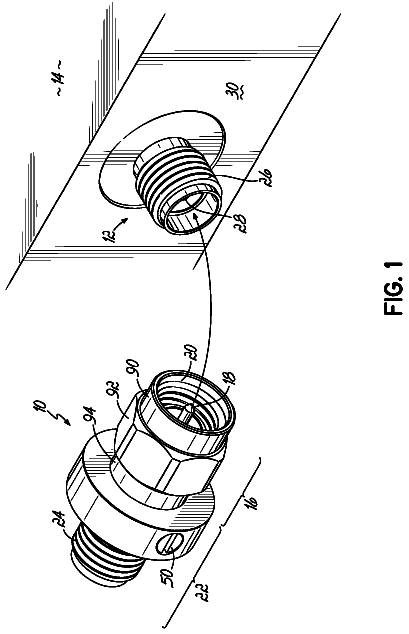
Connector and cable with torque-limiting features
A connector includes separate portions that rotatably couple together and form a connector.
US 9,999,124 B2 · Assignee: INTERNATIONAL BUSINESS MACHINES CORPORATION · Inventors: Busby; James A. et al.
Sheet 1 of 14 from the published document. All sheets in the USPTO PDF
Tamper-respondent assemblies with regions of increased susceptibility to a tamper event are provided, which include one or more tamper-detect sensors, one or more conductive traces, and an adhesive. The tamper-detect sensor(s) facilitates defining a secure volume about one or more electronic components to be protected, and the conductive trace(s) forms, at least in part, a tamper-detect network of the tamper-respondent assembly. The conductive trace(s) is disposed, at least in part, on the tamper-detect sensor(s). The adhesive contacts the conductive trace(s) on the tamper-detect sensor(s), and is disposed, at least in part, between and couples a surface of the tamper-detect sensor(s) to another surface of the assembly. Together, the tamper-detect sensor(s), conductive trace(s), and adhesive are a subassembly, with the subassembly being configured with multiple regions of increased susceptibility to breaking of the conductive trace(s) with a tamper event through the subassembly.
Many activities require secure electronic communications. To facilitate secure electronic communications, an encryption/decryption system may be implemented on an electronic assembly or printed circuit board assembly that is included in equipment connected to a communications network. Such an electronic assembly is an enticing target for malefactors since it may contain codes or keys to decrypt intercepted messages, or to encode fraudulent messages. To prevent this, an electronic assembly may be mounted in an enclosure, which is then wrapped in a security sensor and encapsulated with polyurethane resin. A security sensor may be, in one or more embodiments, a web or sheet of insulating material with circuit elements, such as closely-spaced, conductive lines fabricated on it. The circuit elements are disrupted if the sensor is torn, and the tear can be sensed in order to generate an alarm
1 of 14 drawing sheets so far from the published document, cropped to the drawing. Every sheet is in the USPTO PDF.
What the patent claimed, word for word. All of it is now free to use.
Many activities require secure electronic communications. To facilitate secure electronic communications, an encryption/decryption system may be implemented on an electronic assembly or printed circuit board assembly that is included in equipment connected to a communications network. Such an electronic assembly is an enticing target for malefactors since it may contain codes or keys to decrypt intercepted messages, or to encode fraudulent messages. To prevent this, an electronic assembly may be mounted in an enclosure, which is then wrapped in a security sensor and encapsulated with polyurethane resin. A security sensor may be, in one or more embodiments, a web or sheet of insulating material with circuit elements, such as closely-spaced, conductive lines fabricated on it. The circuit elements are disrupted if the sensor is torn, and the tear can be sensed in order to generate an alarm signal. The alarm signal may be conveyed to a monitor circuit in order to reveal an attack on the integrity of the assembly. The alarm signal may also trigger an erasure of encryption/decryption keys stored within the electronic assembly.
Provided herein, in one or more aspects, is a tamper-respondent assembly which includes: a tamper-detect sensor, at least one conductive trace, and an adhesive. The tamper-detect sensor facilitates defining a secure volume about at least one electronic component to be protected, and the at least one conductive trace forms, at least in part, at least one tamper-detect network of the tamper-respondent assembly. The at least one conductive trace is exposed, at least in part, on the tamper-detect sensor. The adhesive contacts the at least one conductive trace on the at least one tamper-detect sensor, and is disposed, at least in part, between and couples a surface of the tamper-detect sensor to another surface of the tamper-respondent assembly. Together, the tamper-detect sensor, at least one conductive trace, and adhesive are a subassembly of the tamper-respondent assembly, and the subassembly is configured with multiple regions of increased susceptibility to breaking of the at least one conductive trace with a tamper event through the subassembly.
In one or more other aspects, a tamper-respondent assembly is provided which includes: an electronic enclosure, a tamper-detect sensor, at least one conductive trace, and an adhesive. The electronic enclosure is to enclose, at least in part, at least one electronic component to be protected, and includes an inner surface. The tamper-detect sensor, which includes at least one flexible layer with tamper-detect circuit lines, covers, at least in part, the inner surface of the electronic enclosure and facilitates defining a secure volume about the at least one electronic component. The at least one conductive trace forms, at least in part, at least one tamper-detect network of the tamper-respondent assembly, and is exposed, at least in part, on the tamper-detect sensor. The adhesive contacts the at least one conductive trace on the at least one tamper-detect sensor, and is disposed, at least in part, between and couples a surface of the tamper-detect sensor to another surface of the tamper-respondent assembly. Together, the tamper-detect sensor, at least one conductive trace, and adhesive are a subassembly of the tamper-respondent assembly, and the subassembly is configured with multiple regions of increased susceptibility to breaking of the at least one conductive trace with a tamper event through the subassembly.
In one or more further aspects, a fabrication method is provided which includes fabricating a tamper-respondent assembly. The fabricating of the tamper-respondent assembly includes: providing a tamper-detect sensor to facilitate defining a secure volume about at least one electronic component to be protected; providing at least one conductive trace forming, at least in part, at least one tamper-detect network of the tamper-respondent assembly, the at least one conductive trace being disposed, at least in part, on the tamper-detect sensor; providing an adhesive contacting the at least one conductive trace on the tamper-detect sensor, the adhesive being disposed, at least in part, between and coupling a surface of the tamper-detect sensor to another surface of the tamper-respondent assembly; and the tamper-detect sensor, at least one conductive trace, and adhesive being a subassembly of the tamper-respondent assembly, the subassembly being configured with multiple regions of increased susceptibility to breaking of the at least one conductive trace with a tamper event through the subassembly.
Additional features and advantages are realized through the techniques of the present invention. Other embodiments and aspects of the invention are described in detail herein and are considered a part of the claimed invention.
One or more aspects of the present invention are particularly pointed out and distinctly claimed as examples in the claims at the conclusion of the specification. The foregoing and other objects, features, and advantages of the invention are apparent from the following detailed description taken in conjunction with the accompanying drawings in which:
FIG. 1 is a partial cut-away of one embodiment of a tamper-proof electronic package;
FIG. 2 depicts one embodiment of a tamper-detect sensor with conductive lines forming, at least in part, at least one tamper-detect network, in accordance with one or more aspects of the present invention;
FIG. 3A is a cross-sectional elevational view of another embodiment of a tamper-proof electronic package, or tamper-respondent assembly, which includes (in part) an enclosure, and a multilayer circuit board with an embedded tamper-detect sensor, in accordance with one or more aspects of the present invention;
FIG. 3B is a top plan view of the multilayer circuit board of FIG. 3A , depicting one embodiment of the secure volume defined, in part, within the multilayer circuit board, in accordance with one or more aspects of the present invention;
FIG. 4 is a partial cross-sectional elevational view of a more detailed embodiment of the tamper-respondent assembly of FIGS. 3A & 3B comprising (in part) an enclosure and a multilayer circuit board with embedded tamper-detect sensor, in accordance with one or more aspects of the present invention;
FIG. 5 depicts one embodiment of a process of fabricating a multilayer circuit board with an embedded tamper-detect sensor, in accordance with one or more aspects of the present invention;
FIG. 6 is an isometric view of one embodiment of a tamper-respondent assembly, in accordance with one or more aspects of the present invention;
FIG. 7A depicts an underside, perspective view of one embodiment of an electronic enclosure and tamper-detect sensor subassembly of a tamper-respondent assembly, in accordance with one or more aspects of the present invention;
FIG. 7B depicts an exploded view of the subassembly of FIG. 7A , in accordance with one or more aspects of the present invention;
FIG. 8A is a cross-sectional elevational view of another embodiment of a tamper-respondent assembly including first and second tamper-detect sensors secured to an inner surface of an electronic enclosure, in accordance with one or more aspects of the present invention;
FIG. 8B is an isometric view of one embodiment of an inner-main-surface, tamper-detect sensor with one or more conductive traces in one or more bond regions thereof, in accordance with one or more aspects of the present invention;
FIG. 8C is a cross-sectional elevational view of the tamper-respondent assembly of FIG. 8A , illustrating an attempted line of attack through the electronic enclosure and adhesive encountering the one or more conductive traces, in accordance with one or more aspects of the present invention;
FIG. 9A is an enlarged, cross-sectional elevational view of a further embodiment of a tamper-respondent assembly including first and second tamper-detect sensors secured to an inner surface of an electronic enclosure, in accordance with one or more aspects of the present invention;
FIG. 9B is a cross-sectional elevational view of the tamper-respondent assembly of FIG. 9A , illustrating an attempted line of attack through the electronic enclosure and the adhesive, again encountering the one or more conductive traces, in accordance with one or more aspects of the present invention;
FIG. 10A is a plan view of one embodiment of a conductive trace and tamper-detect sensor subassembly of a tamper-respondent assembly, such as depicted in FIGS. 8A-9A , with the subassembly being configured with multiple regions of increased susceptibility to breaking of the conductive trace with a tamper event into the tamper-respondent assembly at a bond line of the subassembly to another surface of the tamper-respondent assembly, in accordance with one or more aspects of the present invention;
FIG. 10B depicts the subassembly of FIG. 10A , illustrating multiple breaks in the conductive trace based on an attempted tamper event into the tamper-respondent assembly at the bond line of the subassembly to another surface of the tamper-respondent assembly, in accordance with one or more aspects of the present invention;
FIG. 11A is a cross-sectional elevational view of an alternate approach for configuring a subassembly, which includes first and second tamper-detect sensors, an adhesive, and a conductive trace, with multiple regions of increased susceptibility to breaking of the conductive trace with a tamper event through the subassembly, in accordance with one or more aspects of the present invention; and
FIG. 11B depicts a cross-sectional plan view of the subassembly of FIG. 11A , taken along line 11 B- 11 B thereof, in accordance with one or more aspects of the present invention.
Aspects of the present invention and certain features, advantages, and details thereof, are explained more fully below with reference to the non-limiting example(s) illustrated in the accompanying drawings. Descriptions of well-known materials, fabrication tools, processing techniques, etc., are omitted so as not to unnecessarily obscure the invention in detail. It should be understood, however, that the detailed description and the specific example(s), while indicating aspects of the invention, are given by way of illustration only, and are not by way of limitation. Various substitutions, modifications, additions, and/or arrangements, within the spirit and/or scope of the underlying inventive concepts will be apparent to those skilled in the art for this disclosure. Note further that reference is made below to the drawings, which are not drawn to scale for ease of understanding, wherein the same reference numbers used throughout different figures designate the same or similar components. Also, note that numerous inventive aspects and features are disclosed herein, and unless otherwise inconsistent, each disclosed aspect or feature is combinable with any other disclosed aspect or feature as desired for a particular application, for instance, for establishing a secure volume about an electronic component(s) or electronic assembly to be protected.
Reference is first made to FIG. 1 , which illustrates one approach for an electronic package 100 configured as a tamper-proof electronic package for purposes of discussion. In the depicted embodiment, an electronic assembly enclosure 110 is provided containing, for instance, an electronic assembly, which in one embodiment may include a plurality of electronic components, such as an encryption and/or decryption module and associated memory. The encryption and/or decryption module may include security-sensitive information with, for instance, access to the information stored in the module requiring use of a variable key, and with the nature of the key being stored in the associated memory within the enclosure.
In one or more implementations, a tamper-proof electronic package or tamper-respondent assembly, such as depicted, is configured or arranged to detect attempts to tamper with or penetrate into electronic assembly enclosure 110 . Accordingly, electronic assembly enclosure 110 also includes, for instance, a monitor circuit which, if tampering is detected, activates an erase circuit to erase information stored within the associated memory, as well as the encryption and/or decryption module within the communications card. These components may be mounted on, and interconnected by, a multilayer circuit board, such as a printed circuit board or other multilayer substrate, and be internally or externally powered via a power supply provided within the electronic assembly enclosure.
In the embodiment illustrated, and as one example only, electronic assembly enclosure 110 may be surrounded by a tamper-detect sensor 120 , an encapsulant 130 , and an outer, thermally conductive enclosure 140 . In one or more implementations, tamper-detect sensor 120 may include a tamper-detection laminate that is folded around electronic assembly enclosure 110 , and encapsulant 130 may be provided in the form of a molding. Tamper-detect sensor 120 may include various detection layers, which are monitored through, for instance, a ribbon cable by the enclosure monitor, against attempts to penetrate enclosure 110 and damage the enclosure monitor or erase circuit, before information can be erased from the encryption module. The tamper-detect sensor may be, for example, any such article commercially available or described in various publications and issued patents, or any enhanced article such as disclosed herein.
By way of example, tamper-detect sensor 120 may be formed as a tamper-detection laminate including a number of separate layers with, for instance, an outermost lamination-detection layer including a matrix of, for example, diagonally-extending or sinusoidally-extending, conductive or semi-conductive lines printed onto a regular, thin insulating film. The matrix of lines forms a number of continuous conductors which would be broken if attempts are made to penetrate the film. The lines may be formed, for instance, by printing conductive traces onto the film and selectively connecting the lines on each side, by conductive vias, near the edges of the film. Connections between the lines and an enclosure monitor of the communications card may be provided via, for instance, one or more ribbon cables. The ribbon cable itself may be formed of lines of conductive material printed onto an extension of the film, if desired. Connections between the matrix and the ribbon cable may be made via connectors formed on one edge of the film. As noted, the laminate may be wrapped around the electronic assembly enclosure to define the tamper-detect sensor 120 surrounding enclosure 110 .
In one or more implementations, the various elements of the laminate may be adhered together and wrapped around enclosure 110 , in a similar manner to gift-wrapping a parcel, to define the tamper-detect sensor shape 120 . The assembly may be placed in a mold which is then filled with, for instance, cold-pour polyurethane, and the polyurethane may be cured and hardened to form an encapsulant 130 . The encapsulant may, in one or more embodiments, completely surround the tamper-detect sensor 120 and enclosure 110 , and thus form a complete environmental seal, protecting the interior of the enclosure. The hardened polyurethane is resilient and increases robustness of the electronic package in normal use. Outer, thermally conductive enclosure 140 may optionally be provided over encapsulant 130 to, for instance, provide further structural rigidity to the electronic package.
When considering tamper-proof packaging, the electronic package needs to maintain defined tamper-proof requirements, such as those set forth in the National Institutes of Standards and Technology (NIST) Publication FIPS 140 - 2 , which is a U.S. Government Computer Security Standard, used to accredit cryptographic modules. The NIST FIPS 140 - 2 defines four levels of security, named Level 1 to Level 4, with Security Level 1 providing the lowest level of security, and Security Level 4 providing the highest level of security. At Security Level 4, physical security mechanisms are provided to establish a complete envelope of protection around the cryptographic module, with the intent of detecting and responding to any unauthorized attempt at physical access. Penetration of the cryptographic module enclosure from any direction has a very high probability of being detected, resulting in the immediate zeroization of all plain text critical security parameters (CSPs). Security Level 4 cryptographic modules are useful for operation in physically unprotected environments. Security Level 4 also protects a cryptographic module against a security compromise due to environmental conditions or fluctuations outside the module's normal operating ranges for voltage and temperature. Intentional excursions beyond the normal operating ranges may be used by an attacker to thwart the cryptographic module's defenses. The cryptographic module is also required to either include specialized environmental protection features designed to detect fluctuations and zeroize, critical security parameters, or to undergo rigorous environmental failure testing to provide reasonable assurances that the module will not be affected by fluctuations outside the normal operating range in a manner than can compromise the security of the module.
To address the demands for ever-improving anti-intrusion technology, and the higher-performance encryption/decryption functions being provided, enhancements to the tamper-proof, tamper-evident packaging for the electronic component(s) or assembly at issue are desired.
Numerous enhancements are described herein to, for instance, tamper-proof electronic packages or tamper-respondent assemblies. As noted, the numerous inventive aspects described herein may be used singly, or in any desired combination. Additionally, in one or more implementations, the enhancements described herein may be provided to work within defined space limitations for existing packages.
Disclosed hereinbelow with reference to FIGS. 2-11B are various approaches and/or enhancements to creating, for instance, a secure volume for accommodating one or more electronic components, such as one or more encryption and/or decryption modules and associated components of, for instance, a communications card or other electronic assembly to be protected.
FIG. 2 depicts a portion of one embodiment of a tamper-detection layer 205 (or laser and pierce-respondent layer) of a tamper-detect sensor 200 or security sensor, such as discussed herein. In FIG. 2 , tamper-detection layer 205 includes circuit lines or traces 201 provided on one or both opposite sides of a flexible layer 202 , which in one or more embodiments, may be a flexible insulating layer or film. FIG. 2 illustrates circuit lines 201 on, for instance, one side of flexible layer 202 , with the traces on the opposite side of the film being, for instance, the same pattern, but (in one or more embodiments) offset to lie directly below spaces 203 , between circuit lines 201 . As described below, the circuit lines on one side of the flexible layer may be of a line width W.sub.l and have a pitch or line-to-line spacing W.sub.s such that piercing of the layer 205 at any point results in damage to at least one of the circuit lines traces 201 . In one or more implementations, the circuit lines may be electrically connected in-series or parallel to define one or more conductors which may be electrically connected in a network to an enclosure monitor, which may, in one or more implementations, monitor the resistance of the lines. Detection of an increase, or other change, in resistance, caused by cutting or damaging one of the traces, will cause information within the encryption and/or decryption module to be erased. Providing conductive lines 201 in a pattern, such as a sinusoidal pattern, may advantageously make it more difficult to breach tamper-detection layer 205 without detection. Note, in this regard, that conductive lines 201 could be provided in any desired pattern. For instance, in an alternate implementation, conductive lines 201 could be provided as parallel, straight conductive lines, if desired, and the pattern or orientation of the pattern may vary between sides of a layer, and/or between layers.
As noted, as intrusion technology continues to evolve, anti-intrusion technology needs to continue to improve to stay ahead. In one or more implementations, the above-summarized tamper-detect sensor 200 of FIG. 2 may be disposed over an outer surface of an electronic enclosure, such as an electronic enclosure described above in connection with FIG. 1 . Alternatively, as described further herein, the tamper-detect sensor may cover or line an inner surface of an electronic enclosure to provide a secure volume about at least one electronic component to be protected. Still further, the tamper-detect sensor, or more particularly, the tamper-detect circuit(s) of the sensor, could be embedded within a multilayer circuit board described below.
In one or more aspects, disclosed herein is a tamper-detect sensor 200 with circuit lines 201 having reduced line widths W.sub.l of, for instance, 200 μm, or less, such as less than or equal to 100 μm, or even more particularly, in the range of 30-70 μm. This is contrasted with conventional trace widths, which are typically on the order of 250 μm or larger. Commensurate with reducing the circuit line width W.sub.l, line-to-line spacing width W.sub.s 203 is also reduced to less than or equal to 200 μm, such as less than or equal to 100 μm, or for instance, in a range of 30-70 μm. Advantageously, by reducing the line width W.sub.l and line-to-line spacing W.sub.s of circuit lines 201 within tamper-detect sensor 200 , the circuit line width and pitch is on the same order of magnitude as the smallest intrusion instruments currently available, and therefore, any intrusion attempt will necessarily remove a sufficient amount of a circuit line(s) to cause resistance to change, and thereby the tamper intrusion to be detected. Note that, by making the circuit line width of the smaller dimensions disclosed herein, any cutting or damage to the smaller-dimensioned circuit line will also be more likely to be detected, that is, due to a greater change in resistance. For instance, if an intrusion attempt cuts a 100 μm width line, it is more likely to reduce the line width sufficiently to detect the intrusion by a change in resistance. A change in a narrower line width is more likely to result in a detectable change in resistance, compared with, for instance, a 50% reduction in a more conventional line width of 350 μm to, for instance, 175 μm. The smaller the conductive circuit line width becomes, the more likely that a tampering of that line will be detected.
Note also that a variety of materials may advantageously be employed to form the circuit lines when implemented using resistance monitoring. For instance, the circuit lines may be formed of a conductive ink (such as a carbon-loaded conductive ink) printed onto one or both opposite sides of one or more of the flexible layers 202 in a stack of such layers. Alternatively, a metal or metal alloy could be used to form the circuit lines, such as copper, silver, intrinsically conductive polymers, carbon ink, or nickel-phosphorus (NiP), such as Omega-Ply®, offered by Omega Technologies, Inc. of Culver City, Calif. (USA), or nickel-chrome, such as Ticer™ offered by Ticer Technologies, Chandler, Ariz. (USA). Note that the process employed to form the fine circuit lines or traces on the order described herein is dependent, in part, on the choice of material used for the circuit lines. For instance, if copper circuit lines are being fabricated, then additive processing, such as plating up copper traces, or subtractive processing, such as etching away unwanted copper between trace lines, may be employed. By way of further example, if conductive ink is employed as the circuit line material, fine circuit lines on the order disclosed herein can be achieved by focusing on the rheological properties of the conductive ink formulation. Further, rather than simple pneumatics of pushing conductive ink through an aperture in a stencil with a squeegee, the screen emulsion may be characterized as very thin (for instance, 10 to 30 μm), and a squeegee angle may be used such that the ink is sheared to achieve conductive ink breakaway rather than pumping the conductive ink through the screen apertures. Note that the screen for fine line width printing such as described herein may have the following characteristics in one specific embodiment: a fine polyester thread for both warp and weave on the order of 34-48 micrometers; a thread count between 250-320 threads per inch; a mesh thickness of, for instance, 53-81 micrometers; an open area between threads that is at least 1.5× to 2.0× the conductive ink particle size; and to maintain dimensional stability of the print, the screen snap-off is kept to a minimum due the screen strain during squeegee passage.
In a further aspect, the flexible layer 202 itself may be further reduced in thickness from a typical polyester layer by selecting a crystalline polymer to form the flexible layer or substrate. By way of example, the crystalline polymer could comprise polyvinylidene difluoride (PVDF), or Kapton, or other crystalline polymer material. Advantageously, use of a crystalline polymer as the substrate film may reduce thickness of the flexible layer 202 to, for instance, 50 micrometers thick from a more conventional amorphous polyester layer of, for instance, 125-150 micrometers. A crystalline polymer can be made much thinner, while still maintaining structural integrity of the flexible substrate, which advantageously allows for far more folding, and greater reliability of the sensor after folding. Note that the radius of any fold or curvature of the sensor is necessarily constrained by the thickness of the layers comprising the sensor. Thus, by reducing the flexible layer thickness to, for instance, 50 micrometers, then in a four tamper-detection layer stack, the stack thickness can be reduced from, for instance, 500 micrometers in the case of a typical polyester film, to 250 micrometers or less with the use of crystalline polymer films.
FIGS. 3A & 3B depict one embodiment of a tamper-proof electronic package 300 , or tamper-respondent assembly, which comprises one or more electronic components, such as a circuit 315 and/or electronic devices (or elements) 302 to be protected, in accordance with one or more further aspects of the present invention.
Referring collectively to FIGS. 3A & 3B , circuit 315 resides on or is embedded within a multilayer circuit board 310 , which also has an embedded tamper-detect sensor 311 that facilitates defining, in part, a secure volume 301 associated with multilayer circuit board 310 that (in one or more embodiments) extends into multilayer circuit board 310 . In particular, in the embodiment of FIGS. 3A & 3B , secure volume 301 may exist partially within multilayer circuit board 310 , and partially above multilayer circuit board 310 . One or more electronic devices 302 are mounted to multilayer circuit board 310 within secure volume 301 and may include, for instance, one or more encryption modules and/or decryption modules, and/or associated components, to be protected within the tamper-proof electronic package. In one or more implementations, the one or more electronic components to be protected may include, for instance, a secure communications card of a computer system.
Tamper-proof electronic package 300 further includes an enclosure 320 , such as a pedestal-type enclosure, mounted to multilayer circuit board 310 within, for instance, a continuous groove (or trench) 312 formed within an upper surface of multilayer circuit board 310 , and secured to the multilayer circuit board 310 via, for instance, a structural adhesive disposed within continuous groove 312 . In one or more embodiments, enclosure 320 may include a thermally conductive material and operate as a heat sink for facilitating cooling of the one or more electronic components 302 within the secure volume. A security mesh or tamper-detect sensor 321 may be associated with enclosure 320 , for example, wrapping around the inner surface of enclosure 320 , to facilitate defining, in combination with tamper-detect sensor 311 embedded within multilayer circuit board 310 , secure volume 301 . In one or more implementations, tamper-detect sensor 321 may extend down into continuous groove 312 in multilayer circuit board 310 and may, for instance, even wrap partially or fully around the lower edge of enclosure 320 within continuous groove 312 to provide enhanced tamper detection where enclosure 320 couples to multilayer circuit board 310 . In one or more implementations, enclosure 320 may be securely affixed to multilayer circuit board 310 using, for instance, a bonding material such as an epoxy or other adhesive.
Briefly described, tamper-detect sensor 321 may include, in one or more examples, one or more tamper-detection layers which include circuit lines or traces provided on one or both sides of a flexible layer, which in one or more implementations, may be a flexible insulating layer or film. The circuit lines on one or both sides of the flexible layer may be of a line width and have a pitch or line-to-line spacing such that piercing of the layer at any point results in damage to one or more of the circuit lines or traces. In one or more implementations, the circuit lines may define one or more conductors which may be electrically connected in a network to an enclosure monitor or detector 303 , which monitors, for instance, resistance on the lines, or as described below, in the case of conductors, may monitor for a nonlinearity, or non-linear conductivity change, on the conductive lines. Detection of a change in resistance or a nonlinearity caused by cutting or damaging one or more of the lines, will cause information within the secure volume to be automatically erased. The conductive lines of the tamper-detect sensor may be in any desired pattern, such as a sinusoidal pattern, to make it more difficult to breach the tamper-detection layer without detection.
For resistive monitoring, a variety of materials may be employed to form the circuit lines. For instance, the circuit lines may be formed of a metal or metal alloy, such as copper, or silver, or could be formed, for example, of an intrinsically-conductive polymer, carbon ink, or nickel phosphorous (NiP), or Omega-Ply®, offered by Omega Technologies, Inc., of Culver City, Calif. (USA), or Ticer™, offered by Ticer Technologies, Chandler, Ariz. (USA). The process employed to form the fine circuit lines or traces is dependent, in part, on the choice of materials used for the circuit lines. For instance, if copper circuit lines are fabricated, then additive processing, such as plating of copper traces, or subtractive processing, such as etching away unwanted copper between trace lines, may be employed.
As noted, in one or more implementations, the circuit lines of the tamper-detect sensor(s) lining the inner surface(s) of enclosure 320 , or even printed directly onto one or more layers formed over the inner surface of enclosure 320 , may be connected to define one or more detect networks.
If a flexible layer is used over the inner surface of enclosure 320 , then the flexible layer may be formed of a crystalline polymer material. For instance, the crystalline polymer could comprise polyvinylidene difluoride (PVDF), or Kapton, or other crystalline polymer material. Advantageously, a crystalline polymer may be made much thinner, while still maintaining structural integrity of the flexible substrate, which also allows for enhanced folding, and greater reliability of the sensor after folding.
As depicted in FIG. 3B , one or more external circuit connection vias 313 may be provided within multilayer circuit board 310 for electrically connecting to the one or more electronic components within secure volume 301 . These one or more external circuit connection vias 313 may electrically connect to one or more external signal lines or planes (not shown) embedded within multilayer circuit board 310 and extending, for instance, into a secure base region of (or below) secure volume 301 , as explained further below. Electrical connections to and from secure volume 301 may be provided by coupling to such external signal lines or planes within the multilayer circuit board 310 .
As noted, secure volume 301 may be sized to house one or more electronic components to be protected, and may be constructed to extend into multilayer circuit board 310 . In one or more implementations, multilayer circuit board 310 includes electrical interconnect within the secure volume 301 defined in the board, for instance, for electrically connecting one or more tamper-detection layers of the embedded tamper-detect sensor 311 to associated monitor circuitry also disposed within secure volume 301 , along with, for instance, one or more daughter cards, such as memory DIMMs, PCIe cards, processor cards, etc.
Note that the packaging embodiment depicted in FIGS. 3A & 3B is presented by way of example only. Other configurations of enclosure 320 , or multilayer circuit board 310 may be employed, and/or other approaches to coupling enclosure 320 and multilayer circuit board 310 may be used. For instance, in one or more alternate implementations, enclosure 320 may be securely affixed to an upper surface of multilayer circuit board 310 (without a continuous groove) using, for instance, a structural bonding material such as an epoxy or other adhesive.
By way of further example, FIG. 4 depicts a partial cross-sectional elevational view of a more detailed embodiment of tamper-proof electronic package 300 , and in particular, of multilayer circuit board 310 , to which enclosure 320 is secured. In this configuration, the embedded tamper-detect sensor includes multiple tamper-detection layers including, by way of example, at least one tamper-detection mat (or base) layer 400 , and at least one tamper-detection frame 401 . In the example depicted, two tamper-detection mat layers 400 and two tamper-detection frames 401 are illustrated, by way of example only. The lower-most tamper-detection mat layer 400 may be a continuous sense or detect layer extending completely below the secure volume being defined within and/or above multilayer circuit board 310 . One or both tamper-detection mat layers 400 below secure volume 301 may be partitioned into multiple circuit zones. Within each tamper-detection mat layer, or more particularly, within each circuit zone of each tamper-detection mat layer, multiple circuits or conductive traces may be provided in any desired configuration. Further, the conductive traces within the tamper-detection layers may be implemented as, for instance, a resistive layer.
As illustrated, one or more external signal lines or planes 405 may enter secure volume 301 between, in one embodiment, two tamper-detection mat layers 400 , and then electrically connect upwards into the secure volume 301 through one or more conductive vias, arranged in any desired location and pattern. In the configuration depicted, the one or more tamper-detection frames 401 are disposed at least inside of the area defined by continuous groove 312 accommodating the base of enclosure 320 . Together with the tamper-detect sensor(s) 321 associated with enclosure 320 , tamper-detection frames 401 , and tamper-detection mat layers 400 , define secure volume 301 , which may extend, in part, into multilayer circuit board 310 . With secure volume 301 defined, in part, within multilayer circuit board 310 , the external signal line(s) 405 may be securely electrically connected to, for instance, the one or more electronic components mounted to, or of, multilayer circuit board 310 within secure volume 301 . In addition, secure volume 301 may accommodate electrical interconnection of the conductive traces of the multiple tamper-detection layers 400 , 401 , for instance, via appropriate monitor circuitry.
Added security may be provided by extending tamper-detection mat layers 400 (and if desired, tamper-detection frames 401 ) outward past the periphery of enclosure 320 . In this manner, a line of attack may be made more difficult at the interface between enclosure 320 and multilayer circuit board 310 since the attack would need to clear, for instance, tamper-detection mat layers 400 , the enclosure 320 , as well as the tamper-detection frames 401 of the embedded tamper-detect sensor.
Numerous variations on multilayer circuit board 310 of FIGS. 3A-4 are possible. For instance, in one embodiment, the embedded tamper-detect sensor may include one or more tamper-detection mat layers 400 and one or more tamper-detection frames 401 , such as described above, and a tri-plate structure comprising one or more external signal lines or layers sandwiched between an upper ground plane and a lower ground plane. In this configuration, high-speed transfer of signals to and from the secure volume, and in particular, to and from the one or more electronic components resident within the secure volume, would be facilitated.
Note also that, once the secure volume is defined in part within multilayer circuit board 310 , conductive vias within the secure volume between layers of multilayer circuit board 310 may be either aligned, or offset, as desired, dependent upon the implementation. Alignment of conductive vias may facilitate, for instance, providing a shortest connection path, while offsetting conductive vias between layers may further enhance security of the tamper-proof electronic package by making an attack into the secure volume through or around one or more tamper-detection layers of the multiple tamper-detection layers more difficult.
The tamper-detection layers of the embedded tamper-detect sensor formed within the multilayer circuit board of the electronic circuit or electronic package may include multiple conductive traces or lines formed between, for instance, respective sets of input and output contacts or vias at the trace termination points. Any pattern and any number of conductive traces or circuits may be employed in defining a tamper-detection layer or a tamper-detection circuit zone within a tamper-detection layer. For instance, 4, 6, 8, etc., conductive traces may be formed in parallel (or otherwise) within a given tamper-detection layer or circuit zone between the respective sets of input and output contacts to those conductive traces.
In one or more implementations, the multilayer circuit board may be a multilayer wiring board or printed circuit board formed, for instance, by building up the multiple layers of the board. FIG. 5 illustrates one embodiment for forming and patterning a tamper-detection layer within such a multilayer circuit board.
The description continues in the full USPTO document.
About 6,110 words. The USPTO PDF has it with every drawing.
Fees are due 3.5, 7.5 and 11.5 years after grant. This patent expired on June 12, 2026, so the fee marked "not paid" was the one that went unpaid.
TAMPER-RESPONDENT ASSEMBLIES WITH TRACE REGIONS OF INCREASED SUSCEPTIBILITY TO BREAKING
Filed Nov 2016 · published May 2018Tamper-respondent assemblies with trace regions of increased susceptibility to breaking
Filed Nov 2016 · granted Jun 2018Earlier publications, parents and continuations. None of them can still be enforced, or this patent would not be listed.
Prior art cited by the examiner or applicant. Useful when you check your own idea for novelty.
Everything on this page comes from the documents linked above.