Summary
Compounds for use in light-emitting devices are described herein. These compounds may include a biphenyl that includes four substituents, such as benzoxazolyl, benzothiazolyl, or benzimidazolyl substituents.
Some embodiments include a compound represented by Formula 1:
##STR00001## wherein R.sup.1, R.sup.2, R.sup.3, and R.sup.4 are independently optionally substituted benzoxazol-2-yl, optionally substituted benzothiazol-2-yl, or optionally substituted benzimidazol-2-yl; and R.sup.5, R.sup.6, R.sup.7, R.sup.8, R.sup.9, and R.sup.10 are independently H or substituents.
In some embodiments, R.sup.1, R.sup.2, R.sup.3, and R.sup.4 are independently optionally substituted benzoxazol-2-yl, optionally substituted benzothiazol-2-yl, or optionally substituted benzimidazol-2-yl, wherein any substituents of benzoxazol-2-yl, benzothiazol-2-yl, or benzimidazoly-2-yl are independently F, Cl, CH.sub.3, CF.sub.3, CN, OCH.sub.3, NH.sub.2, NO.sub.2, CO.sub.2H, CHO, or OH; and R.sup.5, R.sup.6, R.sup.7, R.sup.8, R.sup.9, and R.sup.10 are independently H, F, Cl, CH.sub.3, CF.sub.3, CN, OCH.sub.3, NH.sub.2, NO.sub.2, CO.sub.2H, CHO (formyl), or OH.
The compounds described herein may be used in light-emitting devices as a nanostructure material or a plurality of nanostructures, a light-extracting material, or both.
Some embodiments include a nanostructure material or a plurality of nanostructures comprising a compound described herein.
Some embodiments include a nanostructure material comprising a compound described herein.
Some embodiments include a nanostructure composition comprising a compound described herein.
Some embodiments include a light-emitting device comprising an anode, a cathode, a light-emitting layer disposed between the anode and the cathode, and a compound described herein. In some embodiments, the compound is part of a nanostructure material disposed between the anode and the cathode. In some embodiments, the device has improved efficiency as compared to a device that is identical in all respects except that it contains no nanostructure material. In some embodiments, the compound is part of a light-extracting material, wherein the anode or the cathode is disposed between the light-emitting layer and the light-extracting material. In some embodiments, the device has improved efficiency as compared to a device that is identical in all respects except that it contains no light-extracting material.
Brief description of the drawings
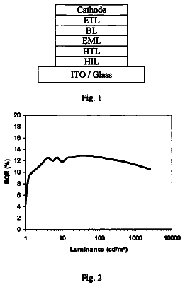
FIG. 1 is a schematic depiction of an embodiment of an organic light-emitting device.
FIG. 2A is a schematic depiction of an embodiment of an organic light-emitting device.
FIG. 2B is a schematic depiction of an embodiment of an organic light-emitting device.
FIG. 3A is a schematic depiction of an embodiment of an organic light-emitting device.
FIG. 3B is a schematic depiction of an embodiment of an organic light-emitting device.
FIG. 4 is a schematic depiction of an embodiment of an organic light-emitting device.
FIG. 5 is a schematic depiction of an embodiment of an organic light-emitting device.
Detailed description
Unless otherwise indicated, when a compound or chemical structural feature such as aryl is referred to as being “optionally substituted,” it includes a feature that has no substituents (i.e. unsubstituted), or a feature that is “substituted,” meaning that the feature has one or more substituents. The term “substituent” has the broadest meaning known to one of ordinary skill in the art, and includes a moiety that replaces one or more hydrogen atoms attached to a parent compound or structural feature. In some embodiments, a substituent may be an ordinary organic moiety known in the art, which may have a molecular weight (e.g. the sum of the atomic masses of the atoms of the substituent) of 15 g/mol to 50 g/mol, 15 g/mol to 100 g/mol, 15 g/mol to 150 g/mol, 15 g/mol to 200 g/mol, 15 g/mol to 300 g/mol, or 15 g/mol to 500 g/mol. In some embodiments, a substituent comprises, or consists of: 0-5 or 0-2 carbon atoms; and 0-5 or 0-3 heteroatoms, wherein each heteroatom may independently be: N, O, S, Si, F, Cl, Br, or I; provided that the substituent includes at least one C, N, O, S, Si, F, Cl, Br, or I atom. Examples of substituents include, but are not limited to, alkyl, alkenyl, alkynyl, heteroalkyl, heteroalkenyl, heteroalkynyl, aryl, heteroaryl, hydroxy, alkoxy, aryloxy, acyl, acyloxy, alkylcarboxylate, thiol, alkylthio, cyano, halo, thiocarbonyl, O-carbamyl, N-carbamyl, O-thiocarbamyl, N-thiocarbamyl, C-amido, N-amido, S-sulfonamido, N-sulfonamido, isocyanato, thiocyanato, isothiocyanato, nitro, silyl, sulfenyl, sulfinyl, sulfonyl, haloalkyl, haloalkoxyl, trihalomethanesulfonyl, trihalomethanesulfonamido, amino, etc.
For convenience, the term “molecular weight” is used with respect to a moiety or part of a molecule to indicate the sum of the atomic masses of the atoms in the moiety or part of a molecule, even though it may not be a complete molecule.
The structures associated with some of the chemical names referred to herein are depicted below. These structures may be unsubstituted, as shown below, or a substituent may independently be in any position normally occupied by a hydrogen atom when the structure is unsubstituted. Unless a point of attachment is indicated by , attachment may occur at any position normally occupied by a hydrogen atom.
##str00002##
Some embodiments include optionally substituted 3,5,3′,5′-tetra(benzoxazol-2-yl)biphenyl; optionally substituted 3,5,3′,5′-tetra(benzothiazol-2-yl)biphenyl; or optionally substituted 3,5,3′,5′-tetra(benzoimidazol-2-yl)biphenyl.
##str00003## ##str00004## ##str00005## ##str00006## ##str00007##
With respect to any relevant formula or structural representation herein, such as Formula 1, R.sup.1 may be optionally substituted benzoxazol-2-yl, optionally substituted benzothiazol-2-yl, or optionally substituted benzimidazol-2-yl. In some embodiments, any substituents of benzoxazol-2-yl, benzothiazol-2-yl, or benzimidazol-2-yl are independently F, Cl, CH.sub.3, CF.sub.3, CN, OCH.sub.3, NH.sub.2, NO.sub.2, CO.sub.2H, CHO, or OH. In some embodiments, any substituents of benzoxazol-2-yl, benzothiazol-2-yl, or benzimidazoly-2-yl are F or Cl. In some embodiments, the benzoxazol-2-yl, the benzothiazol-2-yl, or the benzimidazol-2-yl is unsubstituted.
In some embodiments, R.sup.1 is
##str00008##
With respect to any relevant formula or structural representation herein, such as Formulas 1, 2, 4, 7, 9, 12, and 14, R.sup.2 may be optionally substituted benzoxazol-2-yl, optionally substituted benzothiazol-2-yl, or optionally substituted benzimidazol-2-yl. In some embodiments, any substituents of benzoxazol-2-yl, benzothiazol-2-yl, or benzimidazol-2-yl are independently F, Cl, CH.sub.3, CF.sub.3, CN, OCH.sub.3, NH.sub.2, NO.sub.2, CO.sub.2H, CHO, or OH. In some embodiments, any substituents of benzoxazol-2-yl, benzothiazol-2-yl, or benzimidazoly-2-yl are F or Cl. In some embodiments, the benzoxazol-2-yl, the benzothiazol-2-yl, or the benzimidazol-2-yl is unsubstituted.
In some embodiments, R.sup.2 is
##str00009##
With respect to any relevant formula or structural representation herein, such as Formulas 1, 2, 3, 7, 8, 12, and 13, R.sup.3 may be optionally substituted benzoxazol-2-yl, optionally substituted benzothiazol-2-yl, or optionally substituted benzimidazol-2-yl. In some embodiments, any substituents of benzoxazol-2-yl, benzothiazol-2-yl, or benzimidazol-2-yl are independently F, Cl, CH.sub.3, CF.sub.3, CN, OCH.sub.3, NH.sub.2, NO.sub.2, CO.sub.2H, CHO, or OH. In some embodiments, any substituents of benzoxazol-2-yl, benzothiazol-2-yl, or benzimidazoly-2-yl are F or Cl. In some embodiments, the benzoxazol-2-yl, the benzothiazol-2-yl, or the benzimidazol-2-yl is unsubstituted.
In some embodiments, R.sup.3 is
##str00010##
With respect to any relevant formula or structural representation herein, such as Formulas 1-5, 7-10, and 12-15, R.sup.4 may be optionally substituted benzoxazol-2-yl, optionally substituted benzothiazol-2-yl, or optionally substituted benzimidazol-2-yl. In some embodiments, any substituents of benzoxazol-2-yl, benzothiazol-2-yl, or benzimidazol-2-yl are independently F, Cl, CH.sub.3, CF.sub.3, CN, OCH.sub.3, NH.sub.2, NO.sub.2, CO.sub.2H, CHO, or OH. In some embodiments, any substituents of benzoxazol-2-yl, benzothiazol-2-yl, or benzimidazoly-2-yl are F or Cl. In some embodiments, the benzoxazol-2-yl, the benzothiazol-2-yl, or the benzimidazol-2-yl is unsubstituted.
In some embodiments, R.sup.4 is
##str00011##
With respect to any relevant formula or structural representation herein, such as Formulas 1-16, R.sup.5 may be H, or any substituent, such as F, Cl, CH.sub.3, CF.sub.3, CN, OCH.sub.3, NH.sub.2, NO.sub.2, CO.sub.2H, CHO, or OH. In some embodiments, R.sup.5 is H, F, CF.sub.3, CN, CHO, or OH. In some embodiments, R.sup.5 is H.
With respect to any relevant formula or structural representation herein, such as Formulas 1-16, R.sup.6 may be H, or any substituent, such as F, Cl, CH.sub.3, CF.sub.3, CN, OCH.sub.3, NH.sub.2, NO.sub.2, CO.sub.2H, CHO, or OH. In some embodiments, R.sup.6 is H, F, or CN. In some embodiments, R.sup.6 is H.
With respect to any relevant formula or structural representation herein, such as Formulas 1-16, R.sup.7 may be H, or any substituent, such as F, Cl, CH.sub.3, CF.sub.3, CN, OCH.sub.3, NH.sub.2, NO.sub.2, CO.sub.2H, CHO, or OH. In some embodiments, R.sup.7 is H, F, CF.sub.3, CN, OCH.sub.3, NH.sub.2, CO.sub.2H, CHO, or OH. In some embodiments, R.sup.7 is H.
With respect to any relevant formula or structural representation herein, such as Formulas 1-16, R.sup.8 may be H, or any substituent, such as F, Cl, CH.sub.3, CF.sub.3, CN, OCH.sub.3, NH.sub.2, NO.sub.2, CO.sub.2H, CHO, or OH. In some embodiments, R.sup.8 is H, or F. In some embodiments, R.sup.8 is H.
In some embodiments, R.sup.6 and R.sup.7 are H. In some embodiments, R.sup.6, R.sup.7, and R.sup.8 are H.
With respect to any relevant formula or structural representation herein, such as Formulas 1-16, R.sup.9 may be H, or any substituent, such as F, Cl, CH.sub.3, CF.sub.3, CN, OCH.sub.3, NH.sub.2, NO.sub.2, CO.sub.2H, CHO, or OH. In some embodiments, R.sup.9 is H.
With respect to any relevant formula or structural representation herein, such as Formulas 1-16, R.sup.10 may be H, or any substituent, such as F, Cl, CH.sub.3, CF.sub.3, CN, OCH.sub.3, NH.sub.2, NO.sub.2, CO.sub.2H, CHO, or OH. In some embodiments, R.sup.10 is H, F, CF.sub.3, CN, OCH.sub.3, NH.sub.2, CO.sub.2H, CHO, or OH. In some embodiments, R.sup.10 is H.
In some embodiments, R.sup.5 and R.sup.10 are H. In some embodiments, R.sup.5, R.sup.9, and R.sup.10 are H.
With respect to any relevant formula or structural representation herein, such as Formulas 2-16, R.sup.11 may be H, or any substituent, such as F, Cl, CH.sub.3, CF.sub.3, CN, OCH.sub.3, NH.sub.2, NO.sub.2, CO.sub.2H, CHO, or OH. In some embodiments, R.sup.11 is H, F, CF.sub.3, CN, or CO.sub.2H. In some embodiments, R.sup.11 is H.
With respect to any relevant formula or structural representation herein, such as Formulas 2-16, R.sup.12 may be H, or any substituent, such as F, Cl, CH.sub.3, CF.sub.3, CN, OCH.sub.3, NH.sub.2, NO.sub.2, CO.sub.2H, CHO, or OH. In some embodiments, R.sup.12 is H, F, CF.sub.3, CN, or OH. In some embodiments, R.sup.12 is H.
With respect to any relevant formula or structural representation herein, such as Formulas 2-16, R.sup.13 may be H, or any substituent, such as F, Cl, CH.sub.3, CF.sub.3, CN, OCH.sub.3, NH.sub.2, NO.sub.2, CO.sub.2H, CHO, or OH. In some embodiments, R.sup.13 is H, F, CF.sub.3, OCH.sub.3, NH.sub.2, CO.sub.2H, or OH. In some embodiments, R.sup.13 is H.
With respect to any relevant formula or structural representation herein, such as Formulas 2-16, R.sup.14 may be H, or any substituent, such as F, Cl, CH.sub.3, CF.sub.3, CN, OCH.sub.3, NH.sub.2, NO.sub.2, CO.sub.2H, CHO, or OH. In some embodiments, R.sup.14 is H, F, CF.sub.3, or CN. In some embodiments, R.sup.14 is H.
In some embodiments, R.sup.11 and R.sup.12 are H. In some embodiments, R.sup.11, R.sup.12, R.sup.13 and R.sup.14 are H.
With respect to any relevant formula or structural representation herein, such as Formulas 3, 5, 6, 8, 10, 11, 13, 15, and 16, R.sup.15 may be H, or any substituent, such as F, Cl, CH.sub.3, CF.sub.3, CN, NO.sub.2, CO.sub.2H, or OH. In some embodiments, R.sup.15 is H, F, CF.sub.3, or CN. In some embodiments, R.sup.15 is H or F. In some embodiments, R.sup.15 is H.
With respect to any relevant formula or structural representation herein, such as Formulas 3, 5, 6, 8, 10, 11, 13, 15, and 16, R.sup.16 may be H, or any substituent, such as F, Cl, CH.sub.3, CF.sub.3, CN, NO.sub.2, CO.sub.2H, or OH. In some embodiments, R.sup.16 is H, F, CF.sub.3, or CN. In some embodiments, R.sup.16 is H or CF.sub.3. In some embodiments, R.sup.16 is H.
With respect to any relevant formula or structural representation herein, such as Formulas 3, 5, 6, 8, 10, 11, 13, 15, and 16, R.sup.17 may be H, or any substituent, such as F, Cl, CH.sub.3, CF.sub.3, CN, NO.sub.2, CO.sub.2H, or OH. In some embodiments, R.sup.17 is H, F, CF.sub.3, or CN. In some embodiments, R.sup.17 is H or CH.sub.3. In some embodiments, R.sup.17 is H.
With respect to any relevant formula or structural representation herein, such as Formulas 3, 5, 6, 8, 10, 11, 13, 15, and 16, R.sup.18 may be H, or any substituent, such as F, Cl, CH.sub.3, CF.sub.3, CN, NH.sub.2, NO.sub.2, or OH. In some embodiments, R.sup.18 is H, F, CF.sub.3, or CN. In some embodiments, R.sup.18 is H, F, or CF.sub.3. In some embodiments, R.sup.18 is H.
In some embodiments, R.sup.15 and R.sup.17 are H. In some embodiments, R.sup.15, R.sup.16, R.sup.17 and R.sup.18 are H.
With respect to any relevant formula or structural representation herein, such as Formulas 4-6, 9-11, and 14-16, R.sup.19 may be H, or any substituent, such as F, Cl, CH.sub.3, CF.sub.3, CN, NH.sub.2, NO.sub.2, or OH. In some embodiments, R.sup.19 is H, F, CF.sub.3, CH.sub.3, or CN. In some embodiments, R.sup.19 is H, F, or CH.sub.3. In some embodiments, R.sup.19 is H.
With respect to any relevant formula or structural representation herein, such as Formulas 4-6, 9-11, and 14-16, R.sup.20 may be H, or any substituent, such as F, Cl, CH.sub.3, CF.sub.3, CN, NH.sub.2, NO.sub.2, or OH. In some embodiments, R.sup.20 is H, F, CF.sub.3, CH.sub.3, or CN. In some embodiments, R.sup.20 is H, F, or CF.sub.3. In some embodiments, R.sup.20 is H.
With respect to any relevant formula or structural representation herein, such as Formulas 4-6, 9-11, and 14-16, R.sup.21 may be H, or any substituent, such as F, Cl, CH.sub.3, CF.sub.3, CN, NH.sub.2, NO.sub.2, or OH. In some embodiments, R.sup.21 is H, F, CF.sub.3, CH.sub.3, or CN. In some embodiments, R.sup.21 is H or F. In some embodiments, R.sup.21 is H.
With respect to any relevant formula or structural representation herein, such as Formulas 4-6, 9-11, and 14-16, R.sup.22 may be H, or any substituent, such as F, Cl, CH.sub.3, CF.sub.3, CN, NH.sub.2, NO.sub.2, or OH. In some embodiments, R.sup.22 is H, F, CF.sub.3, CH.sub.3, or CN. In some embodiments, R.sup.22 is H, or CF.sub.3. In some embodiments, R.sup.22 is H.
In some embodiments, R.sup.19 and R.sup.22 are H. In some embodiments, R.sup.19, R.sup.20, R.sup.21 and R.sup.22 are H.
With respect to any relevant formula or structural representation herein, such as Formulas 6, 11, and 16, R.sup.23 may be H, or any substituent, such as F, Cl, CH.sub.3, CF.sub.3, CF.sub.2CF.sub.3, CN, NH.sub.2, NO.sub.2, or OH. In some embodiments, R.sup.23 is H, F, CF.sub.3, CH.sub.3, or CN. In some embodiments, R.sup.23 is H, F, or CH.sub.3. In some embodiments, R.sup.23 is H.
With respect to any relevant formula or structural representation herein, such as Formulas 6, 11, and 16, R.sup.24 may be H, or any substituent, such as F, Cl, CH.sub.3, CF.sub.3, CF.sub.2CF.sub.3, CN, NH.sub.2, NO.sub.2, or OH. In some embodiments, R.sup.24 is H, F, CF.sub.3, CH.sub.3, or CN. In some embodiments, R.sup.24 is H, F, or CF.sub.3. In some embodiments, R.sup.24 is H.
With respect to any relevant formula or structural representation herein, such as Formulas 6, 11, and 16, R.sup.25 may be H, or any substituent, such as F, Cl, CH.sub.3, CF.sub.3, CF.sub.2CF.sub.3, CN, NH.sub.2, NO.sub.2, or OH. In some embodiments, R.sup.25 is H, F, CF.sub.3, CH.sub.3, or CN. In some embodiments, R.sup.25 is H or F. In some embodiments, R.sup.25 is H.
With respect to any relevant formula or structural representation herein, such as Formulas 6, 11, and 16, R.sup.26 may be H, or any substituent, such as F, Cl, CH.sub.3, CF.sub.3, CF.sub.2CF.sub.3, CN, NH.sub.2, NO.sub.2, or OH. In some embodiments, R.sup.26 is H, F, CF.sub.3, CH.sub.3, or CN. In some embodiments, R.sup.26 is H, or CF.sub.3. In some embodiments, R.sup.26 is H.
In some embodiments, R.sup.11, R.sup.18, R.sup.23, and R.sup.28 are H. In some embodiments, R.sup.12, R.sup.17, R.sup.20, and R.sup.24 are H. In some embodiments, R.sup.13, R.sup.16, R.sup.21, and R.sup.25 are H. In some embodiments, R.sup.14, R.sup.15, R.sup.22, and R.sup.26 are H.
With respect to any relevant formula or structural representation herein, such as Formulas 13-16, in some embodiments, R.sup.27 may be H, or any substituent, such as CH.sub.3, CH.sub.2CH.sub.3, or optionally substituted phenyl. In some embodiments, R.sup.27 is H, or phenyl optionally substituted with F, CF.sub.3, CH.sub.3, CN, or a combination thereof. In some embodiments, R.sup.27 is unsubstituted phenyl. In some embodiments, R.sup.27 is H.
With respect to any relevant formula or structural representation herein, such as Formulas 12-16, in some embodiments, R.sup.28 may be H, or any substituent, such as CH.sub.3, CH.sub.2CH.sub.3, or optionally substituted phenyl. In some embodiments, R.sup.28 is H, or phenyl optionally substituted with F, CF.sub.3, CH.sub.3, CN, or a combination thereof. In some embodiments, R.sup.28 is unsubstituted phenyl. In some embodiments, R.sup.28 is H.
With respect to any relevant formula or structural representation herein, such as Formula 16, in some embodiments, R.sup.29 may be H, or any substituent, such as CH.sub.3, CH.sub.2CH.sub.3, or optionally substituted phenyl. In some embodiments, R.sup.29 is H, or phenyl optionally substituted with F, CF.sub.3, CH.sub.3, ON, or a combination thereof. In some embodiments, R.sup.29 is unsubstituted phenyl. In some embodiments, R.sup.29 is H.
With respect to any relevant formula or structural representation herein, such as Formulas 15-16, in some embodiments, R.sup.30 may be H, or any substituent, such as CH.sub.3, CH.sub.2CH.sub.3, or optionally substituted phenyl. In some embodiments, R.sup.30 is H, or phenyl optionally substituted with F, CF.sub.3, CH.sub.3, ON, or a combination thereof. In some embodiments, R.sup.30 is unsubstituted phenyl. In some embodiments, R.sup.30 is H.
In some embodiments, R.sup.27 and R.sup.28 are unsubstituted phenyl. In some embodiments, R.sup.27, R.sup.28, and R.sup.29 are unsubstituted phenyl. In some embodiments, R.sup.27, R.sup.28, R.sup.29, and R.sup.30 are unsubstituted phenyl.
For convenience, a biphenyl that includes four substituents, such as benzoxazolyl, benzothiazolyl, benzimidazolyl, substituents, including a compound of any of Formulas 1-16, is referred to herein as a “subject compound.”
In some embodiments, a subject compound has a highest occupied molecular orbital (HOMO) with an energy of about −6 eV to about −7 eV, about −6 eV to about −6.5 eV, about −6.3 eV to about −6.4 eV, or about −6.35 eV.
In some embodiments, a subject compound has a lowest unoccupied molecular orbital (LUMO) with an energy of about −2 eV to about −3 eV, about −2.5 eV to about −3 eV, about −2.6 eV to about −2.8 eV, or about −2.7 eV.
In some embodiments, a subject compound has an optical band gap of about 3 eV to about 4 eV, about 3.5 eV to about 4 eV, about 3.5 eV to about 3.7 eV, about 3.6 eV to about 3.7 eV, or about 3.65 eV.
In some embodiments, a subject compound has a lowest triplet energy of about 2 eV to about 3 eV, about 2.5 eV to about 3 eV, about 2.5 eV to about 2.7 eV, or about 2.62 eV.
FIG. 1 is a schematic representation of the structure of some embodiments of devices incorporating a subject compound. A light-emitting layer 20 is disposed between a first electrode 2 and a second electrode 4 . A nanostructure material 6 is disposed on light-emitting layer 20 , and a first charge-transport layer 8 is disposed between the nanostructure material 6 and first electrode 2 . An optional second charge-transport layer 9 may be disposed between second electrode 4 and light-emitting layer 20 . Other layers, such as charge injection layers (e.g. electron injection layers or hole injection layers), charge blocking layers (e.g. electron blocking layers or hole blocking layers), hole blocking layers, etc., may also be present in the device.
The character of the electrodes and the charge-transport layers may depend upon the particular device structure. For example, if first electrode 2 is an anode, first charge-transport layer 8 is a hole-transport layer, second electrode 4 is a cathode, and second charge-transport layer 9 , if present, is an electron-transport layer. Conversely, if first electrode 2 is a cathode, first charge-transport layer 8 is an electron-transport layer, second electrode 4 is an anode, and second charge-transport layer 9 , if present, is a hole-transport layer. Thus, a hole-transport layer, if present, may be disposed between a light-emitting layer and an anode, and an electron-transport layer, if present, may be disposed between a light-emitting layer and a cathode.
In addition, the direction of light may depend upon the particular device structure. In some embodiments, the direction of light emitted from the device may depend upon the particular device structure, e.g., top emitting or bottom emitting. In some embodiments, a nanostructure material may be in the path of light emitted from the device. In some embodiments, a nanostructure material may not be in the path of the light emitted from the device. In some embodiments, light 7 can be emitted from the direction of light-emitting layer 20 through the nanostructure material 6 , the first charge-transport layer 8 , and the first electrode 2 . In some embodiments, The path of light emitted by the device may go in the direction away from the nanostructure material 6 .
Nanostructure material, e.g. nanostructure material 6 , may comprise a substituted biphenyl compound, such as a subject compound, and may be in the form of: a plurality of nanostructures disposed on a surface of the light-emitting layer nearest the first charge-transport layer and/or disposed on a surface of the light-emitting layer distal the first charge-transport layer; and/or in a transitional layer comprising a mixture of the first charge-transport material and the nanostructure material, and disposed between the light-emitting layer and the first charge-transport layer.
Nanostructure material, e.g., nanostructure material 6 , may be in the form of a plurality of nanostructures disposed on a surface of or between the light-emitting layer and the hole-transporting layer and/or the electron-transport layer.
Inclusion of nanostructure material may increase luminous efficiency or power efficiency of an OLED by about 10% to about 50% as compared to a similar device without the nanostructure material.
Some embodiments may have a structure represented by FIG. 2A or 2B . A light-emitting layer 20 is disposed between anode 10 and cathode 35 . An optional plurality of nanostructures 50 may be disposed on a surface 21 of light-emitting layer 20 . An optional transitional layer 60 may be disposed between surface 21 of light-emitting layer 20 and hole-transport layer 15 . An optional electron-transport layer 30 may be disposed between light-emitting layer 20 and cathode 35 . An optional light-extracting material 200 may be disposed on anode 10 . In some embodiments, the anode 10 may be disposed on a transparent substrate (not shown). Other layers may also be present.
In some embodiments, light 7 may be emitted from the direction of light-emitting layer 20 through the plurality of nanostructures 50 (if present), transitional layer 60 (if present), hole-transport layer 15 , anode 10 , and light-extracting material 200 (if present) ( FIG. 2A ). In some embodiments, light 7 may be emitted from the direction of the light-emitting layer 20 away from the plurality of nanostructures 50 (if present), through electron-transport of layer 30 (if present) and through cathode 35 ( FIG. 2B ).
Some embodiments may have a structure represented by FIG. 3A or 3B . A light-emitting layer 20 is disposed between an anode 10 and a cathode 35 . An electron-transport layer 30 is disposed between light-emitting layer 20 and cathode 35 . An optional plurality of nanostructures 50 may be disposed on a surface 21 of light-emitting layer 20 . An optional transitional layer 60 may be disposed between surface 21 of light-emitting layer 20 and electron-transport layer 30 . An optional hole-transport layer 15 may be disposed between anode 10 and light-emitting layer 20 . Cathode 35 may be disposed on optional light-extracting material 200 . Light 7 may be emitted from the direction of light-emitting layer 20 through the plurality of nanostructures 50 (if present), transitional layer 60 (if present), electron-transport layer 30 , cathode 35 , and light-extracting material 200 (if present). Other layers may also be present ( FIG. 3A ). In some embodiments, light 7 may be emitted in the direction away from plurality of nanostructures 50 through hole-transport layer 15 (if present), and through anode 10 ( FIG. 3B ).
A plurality of nanostructures, e.g. nanostructures 50 , can comprise a subject compound, and may form a rough interface with the next layer, e.g. a transitional layer or a charge-transport layer. In some embodiments, the plurality of nanostructures 50 have an irregular periodicity within in the matrix material. In some embodiments, the periodicity of the nanostructures in the interface or surface of the nanostructured layer is between about 0.00001 um to about 50 um. In some embodiments, the periodicity may be between about 0.0001 μm and about 1.0 μm. In some embodiments, the periodicity may be between about 0.1 μm and about 10.0 μm.
In some embodiments, the area of the individual nanostructures as projected within the x,y plane or surface 21 can be within about 0.0001 μm.sup.2 to about 1.0 μm.sup.2. In some embodiments the area of the individual nanostructures as projected within the x,y plane can be between about 1 μm.sup.2 to about 3 μm.sup.2. In some embodiments, the area of the individual nanostructures as projected within the x,y plane can be between about 0.04 μm.sup.2 to about 0.150 μm.sup.2.
In some embodiments, a plurality of nanostructures disposed on a surface of a light-emitting layer may have a total mass of about 1 ng to about 500 ng, about 10 ng to about 100 ng, or about 20 ng to about 60 ng for each cm.sup.2 of area of the surface of the light-emitting layer.
In some embodiments, the nominal thickness of a plurality of nanostructures measured by the Quartz Crystal microbalance, which measures the mass deposited onto it, is about 0.0001 nm to about 50 nm or about 0.001 nm to about 10 nm. In some embodiments, the light extraction layer is a discontinuous layer including apertures or voids between islands of light extraction material.
In some embodiments, a plurality of nanostructures thereof may be substantially transparent or substantially translucent.
A plurality of nanostructures may be deposited by vacuum evaporation and can self-assemble into various types of nanostructures described above, depending on the deposition rate. The size and distribution of nanostructures may depend on the deposition rate of the materials. For example, nanostructures may become smaller in all dimensions with increasing deposition rate. In some embodiments, the deposition rate may be about 0.005 nm/s to about 500 nm/s, about 0.005 nm/s, about 0.01 nm/s, about 0.02 nm/s, about 0.03 nm/s, about 0.05 nm/s, about 0.08 nm/s, about 0.1 nm/s, about 0.2 nm/s, about 0.5 nm/s, about 1 nm/s, about 10 nm/s, about 100 nm/s, or any value in a range bounded by, or between, any of these deposition rates. In some embodiments, output enhancement, e.g. the amount of light extracted from the device, may increase with the deposition rate. In some embodiments, output enhancement, e.g. the amount of light extracted from the device, may increase with the deposition rate being between about 0.01 A/s to about 1.5 A/s.
In some embodiments, the area of the nanostructure material disposed within or upon substrate surface, e.g., the light-emitting layer, may vary. In an embodiment, the area of the particles may range between about 0.0001 μm.sup.2 to about 1.0 μm.sup.2. In an embodiment, the area of the particles may range between about 0.001 μm.sup.2 to about 0.5 μm.sup.2.
In some embodiments, the periodicity (separation) of the nanostructure material within or upon the deposed surface, e.g., the light-emitting layer, may vary. In some embodiments, the period of the particles may range between about 0.001 μm to about 20 μm. In some embodiments, the period of the particles may range between about 0.050 μm to about 5 μm.
An anode, e.g. anode 10 , may be a layer comprising a conventional material such as a metal, a mixed metal, an alloy, a metal oxide or a mixed-metal oxide, a conductive polymer, and/or an inorganic material such as a carbon nanotube (CNT). Examples of suitable metals include the Group 1 metals, the metals in Groups 4, 5, 6, and the Group 8-10 transition metals. If the anode layer is to be light-transmitting, metals in Group 10 and 11, such as Au, Pt, and Ag, or alloys thereof; or mixed-metal oxides of Group 12, 13, and 14 metals, such as indium-tin-oxide (ITO), indium-zinc-oxide (IZO), and the like, may be used. If the anode layer is to be light-transmitting, e.g., bottom emitting light-emitting diode construction, the anode layer may include a transparent substrate upon which the light-emitting material is disposed. Suitable transparent materials include, but are not limited to, glass, transparent polymers and transparent plastics. In some embodiments, the anode layer may be an organic material such as polyaniline. The use of polyaniline is described in “Flexible light-emitting diodes made from soluble conducting polymer,” Nature, vol. 357, pp. 477-479 (11 Jun. 1992). In some embodiments, the anode layer can have a thickness in the range of about 1 nm to about 1000 nm.
A cathode, e.g. cathode 35 , may be a layer including a material having a lower work function than the anode layer. Examples of suitable materials for the cathode layer include mixed-metal oxides of Group 12, 13, and 14 metals, such as indium-tin-oxide (ITO), indium-zinc-oxide (IZO), alkali metals of Group 1, Group 2 metals, Group 12 metals, including rare earth elements, lanthanides and actinides, materials such as aluminum, indium, calcium, barium, samarium and magnesium, and combinations thereof. Li-containing organometallic compounds, LiF, and Li.sub.2O may also be deposited between the organic layer and the cathode layer to lower the operating voltage. Suitable low work function metals include but are not limited to Al, Ag, Mg, Ca, Cu, Mg/Ag, LiF/Al, CsF, CsF/Al, ITO, IZO or alloys thereof. In some embodiments, the cathode layer can have a thickness in the range of about 1 nm to about 1000 nm.
A light-emitting layer, e.g. light-emitting layer 20 , may comprise a light-emitting component and a host. Suitable host materials include, but are not limited to those described in co-pending patent applications, U.S. Patent Publication 2011/0140093 (Ser. No. 13/033,473, filed 23 Feb. 2011). In some embodiments, the host may be any of:
##str00012##
The amount of the host in a light-emitting layer may vary. In some embodiments, the amount of a host in a light-emitting layer is in the range of from about 70% to nearly 100% by weight of the light-emitting layer, such as about 90% to about 99%, or about 97% by weight of the light-emitting layer. In some embodiments, the mass of the light-emitting component is about 0.1% to about 10%, about 1% to about 5%, or about 3% of the mass of the light-emitting layer. The light-emitting component may be a fluorescent and/or a phosphorescent compound.
A light-emitting component may comprise an iridium coordination compound such as: bis-{2-[3,5-bis(trifluoromethyl)phenyl]pyridinato-N,C2′}iridium(III)-picolinate; bis(2-[4,6-difluorophenyl]pyridinato-N,C2′)iridium (III) picolinate; bis(2-[4,6-difluorophenyl]pyridinato-N,C2′)iridium(acetylacetonate); Iridium (III) bis(4,6-difluorophenylpyridinato)-3-(trifluoromethyl)-5-(pyridine-2-yl)-1,2,4-triazolate; Iridium (III) bis(4,6-difluorophenylpyridinato)-5-(pyridine-2-yl)-1H-tetrazolate; bis[2-(4,6-difluorophenyl)pyridinato-N,C.sup.2′]iridium(III)tetra(1-pyrazolyl)borate; bis[2-(2′-benzothienyl)-pyridinato-N,C3′]iridium (III)(acetylacetonate); bis[(2-phenylquinolyl)-N,C2′]iridium (III) (acetylacetonate); bis[(1-phenylisoquinolinato-N,C2′)]iridium (III) (acetylacetonate); bisRdibenzo[f,h]quinoxalino-N,C2′)iridium (III)(acetylacetonate); tris(2,5-bis-2′-(9′,9′-dihexylfluorene)pyridine)iridium (III); tris[1-phenylisoquinolinato-N,C2′]iridium (III); tris-[2-(2′-benzothienyl)-pyridinato-N,C3′] iridium (III); tris[1-thiophen-2-ylisoquinolinato-N,C3′]iridium (III); tris[1-(9,9-dimethyl-9H-fluoren-2-yl)isoquinolinato-(N,C3′)iridium (III)); bis(2-phenylpyridinato-N,C2′)iridium(III)(acetylacetonate) [Ir(ppy).sub.2(acac)]; bis(2-(4-tolyl)pyridinato-N,C2′)iridium(III)(acetylacetonate) [Ir(mppy).sub.2(acac)]; bis(2-(4-tert-butyl)pyridinato-N,C2′)iridium (III)(acetylacetonate) [Ir(t-Buppy).sub.2(acac)]; tris(2-phenylpyridinato-N,C2′)iridium (III) [Ir(ppy).sub.3]; bis(2-phenyloxazolinato-N,C2′)iridium (III) (acetylacetonate) [Ir(op).sub.2(acac)]; tris(2-(4-tolyl)pyridinato-N,C2′)iridium(III) [Ir(mppy).sub.3]; bis[2-phenylbenzothiazolato-N,C2′] iridium (III)(acetylacetonate); bis[2-(4-tert-butylphenyl)benzothiazolato-N,C2′]iridium(III)(acetylacetonate); bis[(2-(2′-thienyl)pyridinato-N,C3′)]iridium (III) (acetylacetonate); tris[2-(9.9-dimethylfluoren-2-yl)pyridinato-(N,C3′)]iridium (III); tris[2-(9.9-dimethylfluoren-2-yl)pyridinato-(N,C3′)]iridium (III); bis[5-trifluoromethyl-2-[3-(N-phenylcarbzolyl)pyridinato-N,C2′]iridium(III)(acetylacetonate); (2-PhPyCz).sub.2Ir(III)(acac); etc.
##STR00013## ##STR00014## ##STR00015## ##STR00016## ##STR00017## ##STR00018## ##STR00019##
The thickness of a light-emitting layer may vary. In one embodiment, a light-emitting layer has a thickness in the range of from about 1 nm to about 200 nm, 5 nm to about 150 nm, about 10 nm to about 50 nm, or about 20 nm or about 30 nm.
An optional transitional layer may comprise a mixture of nanostructure material and charge-transport material, such as a hole-transport material or an electron-transport material. Generally, the character of the charge-transport material in the transitional layer depends upon the position of the transitional layer. For example, a transitional layer disposed between a light-emitting layer and a hole-transport layer may comprise a mixture of a hole-transport material and a nanostructure material; and/or a transitional layer disposed between a light-emitting layer and an electron-transport layer may comprise a mixture of an electron-transport material and a nanostructure material. A nanostructure material may have charge-transport properties similar to those of the material with which it is mixed. For example, a nanostructure material with hole-transport properties may be mixed with a hole-transport material in a transitional layer; and/or a nanostructure material with electron-transport properties may be mixed with an electron-transport material in a transitional layer.
The thickness of a transitional layer may vary. In some embodiments, a transitional layer may have a thickness of about 1 nm to about 50 nm, about 5 nm to about 30 nm, or about 8 nm to about 15 nm. In some embodiments, a transition layer is not present.
In a transitional layer, the weight ratio of nanostructure material to charge-transport material may vary, such as about 10:1 to about 1:10, about 1.2:1 to about 1:1.2, or 1:1 to about 1:10, or any ratio in a range bounded by, or between, any of these values.
If present, a hole-transport layer, e.g. hole-transport layer 15 , may be disposed between the anode and the light-emitting layer. A hole-transport layer may comprise at least one hole-transport material. Hole-transport materials may include, but are not limited to, an aromatic-substituted amine, a carbazole, a polyvinylcarbazole (PVK), e.g. poly(9-vinylcarbazole); polyfluorene; a polyfluorene copolymer; poly(9,9-di-n-octylfluorene-alt-benzothiadiazole); poly(paraphenylene); poly[2-(5-cyano-5-methylhexyloxy)-1,4-phenylene]; a benzidine; a phenylenediamine; a phthalocyanine metal complex; a polyacetylene; a polythiophene; a triphenylamine; an oxadiazole; copper phthalocyanine; 1,1-bis(4-bis(4-methylphenyl)aminophenyl)cyclohexane; 2,9-dimethyl-4,7-diphenyl-1,10-phenanthroline; 3,5-bis(4-tert-butyl-phenyl)-4-phenyl[1,2,4]triazole; 3,4,5-triphenyl-1,2,3-triazole; 4,4′,4′-tris(3-methylphenylphenylamino)triphenylamine (MTDATA); N,N′-bis(3-methylphenyl)N,N′-diphenyl-[1,1′-biphenyl]-4,4′-diamine (TPD); 4,4′-bis[N-(naphthyl)-N-phenyl-amino]biphenyl (α-NPD); 4,4′,4″-tris(carbazol-9-yl)-triphenylamine (TCTA); 4,4′-bis[N,N′-(3-tolyl)amino]-3,3′-dimethylbiphenyl (HMTPD); 4,4′-N,N′-dicarbazole-biphenyl (CBP); 1,3-N,N-dicarbazole-benzene (mCP); bis[4-(p,p′-ditolyl-amino)phenyl]diphenylsilane (DTASi); 2,2′-bis(4-carbazolylphenyl)-1,1′-biphenyl (4CzPBP); N,N′N″-1,3,5-tricarbazoloylbenzene (tCP); N,N′-bis(4-butylphenyl)-N,N′-bis(phenyl)benzidine; N,N′-Di(naphthalene-1-yl)-N,N′-diphenyl-benzidine (NPB) or the like.
If present, an electron-transport layer, e.g. electron-transport layer 30 , may be disposed between the cathode and the light-emitting layer. Examples of electron-transport materials may include, but are not limited to, 2-(4-biphenylyl)-5-(4-tert-butylphenyl)-1,3,4-oxadiazole (PBD); 1,3-bis(N,N-t-butyl-phenyl)-1,3,4-oxadiazole (OXD-7), 1,3-bis[2-(2,2′-bipyridine-6-yl)-1,3,4-oxadiazo-5-yl]benzene; 3-phenyl-4-(1′-naphthyl)-5-phenyl-1,2,4-triazole (TAZ); 2,9-dimethyl-4,7-diphenyl-phenanthroline (bathocuproine or BCP); aluminum tris(8-hydroxyquinolate) (Alq3); and 1,3,5-tris(2-N-phenylbenzimidazolyl)benzene; 1,3-bis[2-(2,2′-bipyridine-6-yl)-1,3,4-oxadiazo-5-yl]benzene (BPY-OXD); 3-phenyl-4-(1′-naphthyl)-5-phenyl-1,2,4-triazole (TAZ), 2,9-dimethyl-4,7-diphenyl-phenanthroline (bathocuproine or BCP); and 1,3,5-tris[2-N-phenylbenzimidazol-z-yl]benzene (TPBI). In one embodiment, the electron-transport layer is aluminum quinolate (Alq.sub.3), 2-(4-biphenylyl)-5-(4-tert-butylphenyl)-1,3,4-oxadiazole (PBD), phenanthroline, quinoxaline, 1,3,5-tris[N-phenylbenzimidazol-z-yl] benzene (TPBI), or a derivative or a combination thereof.
The thickness of an electron-transport layer may vary. For example, some electron-transport layers may have a thickness of about 5 nm to about 200 nm, about 10 nm to about 80 nm, or about 20 nm to about 40 nm.
If desired, additional layers may be included in a light-emitting device, such as an electron injecting layer (EIL), a hole-blocking layer (HBL), an exciton-blocking layer (EBL), a hole-injecting layer (HIL), etc. In addition to separate layers, some of these materials may be combined into a single layer.
The description continues in the full USPTO document.
 Lapsed, fee not paid2 drawings

