BACKGROUND OF THE INVENTION Technical Field
The present invention relates to a silicon carbide semiconductor device. Background Art
Silicon carbide (SiC) has attracted attention as a next-generation semiconductor material. Silicon carbide semiconductor devices make it possible to reduce the resistance of the device in the ON state (the on-resistance) to several hundredths of that of conventional silicon (Si) semiconductor devices, can be used in high temperature environments of greater than or equal to 200° C., and offer various other advantages. This is a result of the advantageous properties of the silicon carbide material itself, which in the four-layer hexagonal (4H-SiC) form has a 3.25 eV bandgap that is approximately three times greater than the bandgap of silicon (1.12 eV) as well as a breakdown field strength of nearly an order of magnitude greater than the breakdown field strength of silicon (2 mV/cm to 4 mV/cm).
Various silicon carbide semiconductor devices have previously been prototyped, including rectifying devices such as diodes and switching devices such as transistors and thyristors, for example. However, silicon carbide semiconductor substrates (hereinafter “silicon carbide substrates”) tend to have dislocations in various internal portions. It is known that when a device is formed (manufactured) on a silicon carbide substrate, the recombination of electron-hole pairs during operation of the device induces movement of the dislocations within the silicon carbide substrate and thereby results in growth of stacking faults (see Non-Patent Document 1, for example). These stacking faults negatively affect device performance and increase conduction loss in power modules. Therefore, it is desirable to prevent formation of stacking faults.
One proposed method of preventing formation of stacking faults within silicon carbide substrates involves producing a silicon carbide epitaxial wafer that includes an epitaxial growth layer having low basal plane dislocation density and low stacking fault density in order to improve the quality of the silicon carbide substrate (see Patent Document 1, for example). However, this method cannot yet completely eliminate dislocations and stacking faults within the silicon carbide substrate. Therefore, when a device is formed on the silicon carbide substrate, the stacking faults still expand as described above.
One proposed device for preventing expansion of stacking faults includes stripe-shaped current-limiting regions formed extending parallel to the principal surface of the silicon carbide substrate between the base regions of adjacent cells (the functional unit for elements) in the active region (see Patent Document 2 (paragraphs
to
and FIGS. 1 and 2), for example). In Patent Document 2, forming these current-limiting regions parallel to the step-flow growth direction of the epitaxial growth layer of the silicon carbide substrate prevents expansion of stacking faults.
In another proposed device for preventing expansion of stacking faults, fault stop regions that include a trench-shaped groove going through the epitaxial growth layer of the silicon carbide substrate in the depth direction thereof as well as an insulator filled into that groove are formed in the active region (see Patent Document 3 (paragraph
and FIGS. 1 and 2), for example). In Patent Document 3, these fault stop regions are formed dividing the epitaxial growth layer of the silicon carbide substrate into a matrix pattern in order to prevent expansion of stacking faults.
In yet another proposed device for preventing expansion of stacking faults, current-limiting regions are selectively buried in the epitaxial growth layer (which functions as a drift layer) within the active region (see Patent Document 4 (paragraph
and FIG. 2), for example). In Patent Document 4, when stacking faults that expand from the silicon carbide starting substrate to within the drift layer grown on that starting substrate reach these current-limiting regions, the supply of recombination energy to the stacking faults is stopped, thereby stopping expansion of the stacking faults.
In another proposed device, the gaps between cathode layers arranged in a dotted layout within a collector layer are set to a small value near the center of the semiconductor substrate and set to increasingly large values moving outwards towards the periphery of the semiconductor substrate (see Patent Document 5 (paragraph
and FIGS. 1 and 2), for example). In Patent Document 5, the ratio of the collector layers (which tend to generate heat) per unit area is decreased near the periphery of the semiconductor substrate (which is prone to temperature increases). RELATED ART DOCUMENTS Patent Documents
Patent Document 1: Japanese Patent Application Laid-Open Publication No. 2015-2207 Patent Document 2: Japanese Patent Application Laid-Open Publication No. 2013-232574 Patent Document 3: Japanese Patent Application Laid-Open Publication No. 2004-335720 Patent Document 4: Japanese Patent Application Laid-Open Publication No. 2015-2277 Patent Document 5: Japanese Patent No. 5680299 Non-Patent Document
Non-Patent Document 1: M. Skowronski et al, Degradation of hexagonal silicon-carbide-based bipolar devices, Journal of Applied Physics, (USA), American Institute of Physics, 2006, Vol. 99, 011101-1 to 24 SUMMARY OF THE INVENTION
However, in Patent Documents 2 to 4, forming regions that do not conduct current when the MOSFET is ON (the current-limiting regions or the fault stop regions) within the active region reduces the drift current and thereby reduces the current carrying capability of the device. Moreover, forming trench-shaped grooves in the silicon carbide substrate or selectively forming current-limiting regions or fault stop regions within the silicon carbide substrate increases process complexity. These approaches also increase production costs. In Patent Document 5, the area of the collector layers is adjusted to control temperature increases, which means that this solution cannot be applied to MOSFETs.
The present invention was made to solve the problems in the conventional technologies described above and aims to provide a silicon carbide semiconductor device that makes it possible to maintain current carrying capability as well as inhibit the formation of stacking faults. Accordingly, the present invention is directed to a scheme that substantially obviates one or more of the problems due to limitations and disadvantages of the related art.
Additional or separate features and advantages of the invention will be set forth in the descriptions that follow and in part will be apparent from the description, or may be learned by practice of the invention. The objectives and other advantages of the invention will be realized and attained by the structure particularly pointed out in the written description and claims thereof as well as the appended drawings.
To achieve these and other advantages and in accordance with the purpose of the present invention, as embodied and broadly described, in one aspect, the present disclosure provides a silicon carbide semiconductor device, including: a semiconductor substrate made of silicon carbide, the semiconductor substrate having one or more of first cells and one or more of second cells defined therein; wherein each of the first cells includes: a first semiconductor region of a first conductivity type formed in a surface layer of a first principal surface of the semiconductor substrate; a second semiconductor region of a second conductivity type selectively formed in a surface layer of a second principal surface of the semiconductor substrate; a third semiconductor region of the first conductivity type that is formed between the first semiconductor region and the second semiconductor region, contacts the first semiconductor region and the second semiconductor region, and has a lower impurity concentration than the first semiconductor region; a fourth semiconductor region of the first conductivity type selectively formed within the second semiconductor region; a fifth semiconductor region of the second conductivity type that is selectively formed within the second semiconductor region and has a higher impurity concentration than the second semiconductor region; a gate insulating film formed contacting a region of the second semiconductor region between the third semiconductor region and the fourth semiconductor region; and a gate electrode formed on a side opposite to the second semiconductor region with the gate insulating film between the gate electrode and the second semiconductor region, wherein each of the second cells has the same constructions as the first cell with respect to the first to fifth semiconductor regions except that the fourth semiconductor region of the first conductivity type is absent and that the respective fifth semiconductor regions in the first and second cells may or may not be different in property or dimension, wherein the silicon carbide semiconductor device further includes: a first electrode that contacts the fourth semiconductor region and the fifth semiconductor region of each of the first cells and the fifth semiconductor region of each of the second cells; and a second electrode that contacts the first semiconductor region of each of the first cells and each of the second cells, and wherein a unit total resistance of the fifth semiconductor regions of the second cells, as measured in a depth direction of the semiconductor substrate with respect to a unit area in a surface of the semiconductor substrate, is greater than a unit total resistance of the fifth semiconductor regions of the first cells, as measured in the depth direction of the semiconductor substrate with respect to the unit area in the surface of the semiconductor substrate.
Moreover, in the silicon carbide semiconductor device according to one aspect of the present invention as described above, the first cells are arranged in a plurality in a matrix-shaped layout in an active region, the second cells are arranged in a plurality in a layout that runs along an outer periphery of the active region and surrounds a periphery of the active region, and a surface area of the fifth semiconductor region of each of the second cells is less than a surface area of the fifth semiconductor region of each of the first cells.
Furthermore, in the silicon carbide semiconductor device according to one aspect of the present invention as described above, the first cells are arranged in a plurality in a matrix-shaped layout in an active region, the second cells are arranged in a plurality in a layout that runs along an outer periphery of the active region and surrounds a periphery of the active region, and a number of the second cells per unit area is less than a number of the first cells per unit area.
In addition, in the silicon carbide semiconductor device according to one aspect of the present invention as described above, the second cells are provided in a plurality, and the fifth semiconductor regions of the plurality of second cells are arranged separated from one another at equally spaced intervals.
Moreover, in the silicon carbide semiconductor device according to one aspect of the present invention as described above, the first cells are arranged in a plurality in a matrix-shaped layout in an active region, the second cells are arranged in a plurality in a layout that runs along an outer periphery of the active region and surrounds a periphery of the active region, and an impurity concentration of the fifth semiconductor regions of each of the second cells is less than an impurity concentration of the fifth semiconductor regions of each of the first cells.
Furthermore, in the silicon carbide semiconductor device according to one aspect of the present invention as described above, the first cells are arranged in a plurality in a stripe-shaped layout in an active region, the second cell is provided singly and has a rectangular frame shape that runs along an outer periphery of the active region and surrounds a periphery of the active region, and a width of the fifth semiconductor region of the second cell is less than a width of the fifth semiconductor region of each of the first cells.
In addition, in the silicon carbide semiconductor device according to one aspect of the present invention as described above, the first cells are arranged in a plurality in a stripe-shaped layout in an active region; the second cell is provided singly and has a rectangular frame shape that runs along an outer periphery of the active region and surrounds a periphery of the active region; the fifth semiconductor region of the second cell is arranged in a plurality in a layout that runs along the outer periphery of the active region and surrounds the periphery of the active region; and, among the plurality of fifth semiconductor regions of the second cell, a total surface area of the fifth semiconductor regions that are arranged running in a first direction in which the first cell extends in the stripe shape is less than a surface area of the fifth semiconductor region of each of the first cells.
Moreover, in the silicon carbide semiconductor device according to one aspect of the present invention as described above, the first cells are arranged in a plurality in a stripe-shaped layout in an active region, the second cell is provided singly and has a rectangular planar shape that runs along an outer periphery of the active region and surrounds a periphery of the active region, and an impurity concentration of the fifth semiconductor region of the second cell is less than an impurity concentration of the fifth semiconductor region of each of the first cells.
Furthermore, the semiconductor device according to one aspect of the present invention as described above is mounted in a power module.
The invention as described above makes it possible to reduce current concentration in portions directly beneath the fifth semiconductor regions of the second cells when parasitic diodes in which the fifth semiconductor regions and the second semiconductor regions are the anodes and the third semiconductor region is the cathode turn on. This makes it possible to reduce the incidence of recombination of electron-hole pairs in the portions directly beneath the fifth semiconductor regions of the second cells. In this way, the cell structure of the first cells (which occupy a large area on the chip) can be used to control how easily stacking faults form. Moreover, in the invention as described above, no regions that do not conduct current when the silicon carbide semiconductor device is ON (such as the current-limiting regions or the fault stop regions in the patent documents described above) are formed within the active region, and therefore the current carrying capability of the silicon carbide semiconductor device is not reduced.
The silicon carbide semiconductor device according to the present invention makes it possible to maintain current carrying capability as well as inhibit the formation of stacking faults. It is to be understood that both the foregoing general description and the following detailed description are exemplary and explanatory, and are intended to provide further explanation of the invention as claimed.
Brief description of the drawings
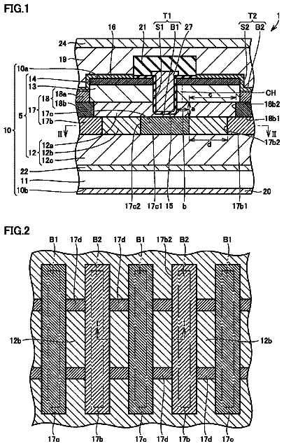
FIG. 1 is a cross-sectional view illustrating the structure of a silicon carbide semiconductor device according to Embodiment 1.
FIG. 2 is a plan view illustrating the planar layout of the primary components in FIG. 1 .
FIG. 3 is a plan view illustrating the planar layout of a silicon carbide semiconductor device according to Comparison Example 1.
FIG. 4 is a characteristic diagram showing the incidence of recombination in a conventional MOSFET.
FIG. 5 is a plan view illustrating the planar layout of the primary components of a silicon carbide semiconductor device according to Embodiment 2.
FIG. 6 is a plan view illustrating the planar layout of the primary components of a silicon carbide semiconductor device according to Embodiment 3.
FIG. 7 is a plan view illustrating the planar layout of a silicon carbide semiconductor device according to Comparison Example 2.
FIG. 8 is a plan view illustrating the planar layout of the primary components of a silicon carbide semiconductor device according to Embodiment 4.
FIG. 9 is a cross-sectional view illustrating the structure of a silicon carbide semiconductor device according to Embodiment 5.
Detailed description of embodiments
Preferred embodiments of a silicon carbide semiconductor device according to the present invention will be described in detail below with reference to the attached drawings. In the present specification and the attached drawings, the letters “n” and “p” are used to indicate whether the majority carriers in a layer or region are electrons or holes, respectively. Moreover, the symbols + and − are appended to the letters n and p to indicate layers or regions having a higher or lower impurity concentration, respectively, than layers or regions in which the + and − symbols are not appended. In the descriptions of the embodiments and the attached drawings, the same reference characters are used to indicate components that are the same, and redundant descriptions of the same components are omitted. Furthermore, the following notation is used for Miller indices in the present specification: the symbol − indicates a bar to be applied to the immediately following index that follows the − symbol; that is, the symbol − is inserted before an index to indicate that that index is negative. Embodiment 1
Next, the structure of a silicon carbide (SiC) semiconductor device according to Embodiment 1 will be described using a MOSFET as an example. FIG. 1 is a cross-sectional view illustrating the structure of the silicon carbide semiconductor device according to Embodiment 1. FIG. 1 illustrates a cross section taken along line A-A′ in FIG. 2 . FIG. 2 is a plan view illustrating the planar layout of the primary components in FIG. 1 . Here, “planar layout” refers to the planar shape and arrangement of the components as viewed from the front surface side of a silicon carbide substrate 10 . FIG. 3 is a plan view illustrating the planar layout of a silicon carbide semiconductor device according to Comparison Example 1. FIG. 4 is a characteristic diagram showing the incidence of recombination in a conventional MOSFET. In FIG. 4 , the horizontal axis represents the depth in a direction going towards the drain electrode side from a boundary (of depth 0 μm) between the semiconductor substrate and the source electrode, and the vertical axis represents the incidence of recombination within the semiconductor substrate.
As illustrated in FIG. 1 , the silicon carbide semiconductor device according to Embodiment 1 includes an active region 21 formed in a center portion of a silicon carbide substrate (semiconductor chip) 10 as well as an edge termination region 22 that surrounds the periphery of the active region 21 . The active region 21 is the region through which current flows when the device is in the ON state. The edge termination region 22 is a region within an n.sup.− drift region 2 that maintains the withstand voltage by reducing the strength of the electric field on the front surface (hereinafter, “substrate front surface”) side of the silicon carbide substrate 10 . In the silicon carbide substrate 10 , a plurality of unit cells (the functional unit for elements) are arranged in a prescribed layout. FIG. 1 illustrates a unit cell (hereinafter, “inner peripheral cell”) 24 a arranged on the outermost side (chip edge side) of the active region 21 , approximately half of another inner peripheral cell 24 a that is adjacent to the inner side (chip center side) of this inner peripheral cell 24 a , and a unit cell (hereinafter, “outermost peripheral cell”) 24 b in a boundary region 23 (described below) (this also applies to FIGS. 6 to 9 ).
The silicon carbide substrate 10 is an epitaxial substrate in which silicon carbide layers 31 and 32 (which will respectively become the n.sup.− drift region 2 and second p-type base regions 4 a and 4 b ) are epitaxially grown in order on the front surface of an n.sup.+ starting substrate 1 made of silicon carbide. The n.sup.+ starting substrate 1 functions as an n.sup.+ drain region. In the active region 21 , a MOS gate structure for the inner peripheral cell 24 a is formed on the front surface side of the silicon carbide substrate 10 (that is, on the surface on the n silicon carbide layer 31 side). More specifically, the MOS gate structure for the inner peripheral cell 24 a includes first and second p-type base regions 3 a and 4 a , an n.sup.+ source region 5 , a p.sup.+ contact region 6 a , an n-type junction FET (JFET) region 7 , a gate insulating film 8 , and a gate electrode 9 .
The first p-type base region 3 a is selectively formed in the surface layer of the n.sup.− silicon carbide layer 31 on the p-type silicon carbide layer 32 side (that is, on the substrate front surface side). Forming the first p-type base region 3 a in an epitaxial growth layer (the n.sup.− silicon carbide layer 31 ) produces a channel with desirable crystalline properties, and the high resulting carrier mobility makes it possible to achieve low on-resistance. The impurity concentration of the first p-type base region 3 a may be 3×10.sup.17/cm.sup.3 to 3×10.sup.18/cm.sup.3, for example. The portion of the n.sup.− silicon carbide layer 31 other than the first p-type base region 3 a is the n.sup.− drift region 2 . The n.sup.+ source region 5 , the p.sup.+ contact region 6 a , and the n-type JFET region 7 are respectively formed selectively within the p-type silicon carbide layer 32 . The n.sup.+ source region 5 and the p.sup.+ contact region 6 a face the first p-type base region 3 a in the depth direction (the vertical direction).
The n.sup.+ source region 5 and the p.sup.+ contact region 6 a contact one another. The p.sup.+ contact region 6 a may go through the p-type silicon carbide layer 32 in the depth direction and reach the first p-type base region 3 a . The impurity concentration of the p.sup.+ contact region 6 a should be set to a value that makes it possible to form ohmic contact (an electrical junction) with a source electrode 12 , such as approximately 1×10.sup.20/cm.sup.3. The n-type JFET region 7 is arranged separated from the n.sup.+ source region 5 on the side of the p.sup.+ contact region 6 a opposite to the n.sup.+ source region 5 . The n-type JFET region 7 is formed by inverting a portion of the p-type silicon carbide layer 32 to n-type using an ion implantation process and goes through the p-type silicon carbide layer 32 in the depth direction to reach the n.sup.− drift region 2 . The n-type JFET region 7 functions as a drift region.
The portion of the p-type silicon carbide layer 32 other than the n.sup.+ source region 5 , the p.sup.+ contact region 6 a , and the n-type JFET region 7 is the second p-type base region 4 a . The impurity concentration of the second p-type base region 4 a may be set to any value lower than the impurity concentration of the first p-type base region 3 a and may thus be set to approximately 3×10.sup.15/cm.sup.3 to approximately 3×10.sup.16/cm.sup.3, for example. The planar layout of the first and second p-type base regions 3 a and 4 a , the n.sup.+ source region 5 , the p.sup.+ contact region 6 a , and the n-type JFET region 7 will be described later. The gate insulating film 8 is formed, spanning from the n.sup.+ source region 5 to the surface of the n-type JFET region 7 , on the surface of the portion of the second p-type base region 4 a that is sandwiched between the n.sup.+ source region 5 and the n-type JFET region 7 . The gate electrode 9 is formed on the gate insulating film 8 .
The region from the widthwise center of one n-type JFET region 7 to the widthwise center of another n-type JFET region 7 that is adjacent to that one n-type JFET region 7 corresponds to one inner peripheral cell 24 a . Here, the width of each n-type JFET region 7 is equal to the distance between adjacent second p-type base regions 4 a . An interlayer insulating film 11 is formed spanning over the entire substrate front surface from the active region 21 to the edge termination region 22 and covering the gate electrode 9 . The source electrode 12 contacts the n.sup.+ source region 5 and the p.sup.+ contact region 6 a via a contact hole formed in the interlayer insulating film 11 and is electrically insulated from the gate electrode 9 by the interlayer insulating film 11 . A drain electrode 13 is formed spanning over the entire rear surface of the silicon carbide substrate 10 (that is, the rear surface of the n.sup.+ starting substrate 1 ).
First and second p-type base regions 3 b and 4 b that have the same configuration as the first and second p-type base regions 3 a and 4 a in the active region 21 are arranged on the front surface side of the silicon carbide substrate 10 in a region (hereinafter, “boundary region”) 23 between the active region 21 and the edge termination region 22 . The first and second p-type base regions 3 b and 4 b face the first and second p-type base regions 3 a and 4 a in the active region 21 with the outermost n-type JFET region 7 sandwiched therebetween. The first and second p-type base regions 3 b and 4 b in the boundary region 23 extend into the edge termination region 22 . A p.sup.+ contact region 6 b is selectively formed, separated from the n-type JFET region 7 , within the second p-type base region 4 b in the boundary region 23 . The impurity concentration of the p.sup.+ contact region 6 b is substantially equal to the impurity concentration of the p.sup.+ contact region 6 a of the inner peripheral cell 24 a.
The p.sup.+ contact region 6 b in the boundary region 23 extracts, to the source electrode 12 , holes that accumulate near the boundary between the n.sup.− drift region 2 and the first p-type base region 3 b while the MOSFET is OFF. Therefore, forming the p.sup.+ contact region 6 b in the boundary region 23 makes it possible to, while the MOSFET is OFF, reduce the current that flows from the substrate rear surface in the edge termination region 22 to the first p-type base region 3 b as well as prevent current that flows inwards from the substrate rear surface in the edge termination region 22 from flowing into the active region 21 . No n.sup.+ source region is formed within the second p-type base region 4 b in the boundary region 23 . The outermost gate insulating film 8 and gate electrode 9 extend onto the surface of the second p-type base region 4 b in the boundary region 23 .
The portion from the widthwise center of the outermost JFET region 7 to a prescribed distance on the outer side (a length d 2 (described later)) corresponds to one unit cell (outermost peripheral cell) 24 b in the boundary region 23 . The outermost peripheral cell 24 b includes the first and second p-type base regions 3 b and 4 b and the p.sup.+ contact region 6 b in the boundary region 23 . The planar layout of the first and second p-type base regions 3 b and 4 b and the p.sup.+ contact region 6 b in the boundary region 23 will be described later. The outermost gate insulating film 8 and gate electrode 9 may extend from the active region 21 into the boundary region 23 . The source electrode 12 extends from the active region 21 into the boundary region 23 and contacts the second p-type base region 4 b and the p.sup.+ contact region 6 b in the boundary region 23 . The end of the source electrode 12 is terminated on the interlayer insulating film 11 at a position further outwards than the p.sup.+ contact region 6 b in the boundary region 23 .
The p-type silicon carbide layer 32 is removed across the entire edge termination region 22 to form a level difference 41 that is lower than the active region 21 and the boundary region 23 (thus receding towards the drain side) in the front surface of the silicon carbide substrate 10 in the edge termination region 22 . In other words, the n.sup.− silicon carbide layer 31 is exposed on the substrate front surface in the edge termination region 22 . A prescribed thickness may be removed from the surface layer of the n.sup.− silicon carbide layer 31 that is exposed on the substrate front surface by the level difference 41 relative to the boundary region 23 . The connecting portion (hereinafter, the “stair in the level difference 41 ”) 41 a between (the upper level and lower level of) the substrate front surface in the boundary region 23 and the edge termination region 22 may be slanted or substantially orthogonal relative to the substrate front surface.
The first p-type base region 3 b in the boundary region 23 (or the first and second p-type base regions 3 b and 4 b in the boundary region 23 ) is exposed along the stair 41 a in the level difference 41 . The second p-type base region 4 b in the boundary region 23 is exposed along the surface layer of the n.sup.− silicon carbide layer 31 that is exposed on the substrate front surface by the level difference 41 relative to the boundary region 23 . Here, “exposed” means arranged contacting the interlayer insulating film 11 on the substrate front surface. Moreover, a voltage withstand structure such as a junction termination extension (JTE) structure is formed in the n.sup.− silicon carbide layer 31 that is exposed on the substrate front surface by the level difference 41 relative to the boundary region 23 , for example.
The JTE structure includes a plurality of p-type regions (here, two regions: first and second JTE regions 42 and 43 ) arranged adjacent to one another in a concentric circle pattern surrounding the periphery of the active region 21 , with the regions arranged further outwards having increasingly lower impurity concentrations. The first JTE region (a p.sup.− region) 42 is formed on the innermost side of the edge termination region 22 and contacts the first p-type base region 3 b in the boundary region 23 . The second JTE region (a p.sup.− region) 43 is formed further outwards than the first JTE region 42 and contacts the first JTE region 42 . The voltage withstand structure is not limited to this example and may be modified in various ways. For example, instead of a JTE structure, a voltage withstand structure that includes a combination of components such as a guard ring, a field plate, and a RESURF portion may be arranged.
Next, the planar layout of the components in the inner peripheral cell 24 a and the outermost peripheral cell 24 b will be described. As illustrated in FIG. 2 , a plurality of the inner peripheral cells 24 a are arranged in a matrix-like planar layout. A plurality of the outermost peripheral cells 24 b are arranged contacting one another in a planar layout that runs along the outer periphery of the active region 21 and surrounds the periphery of the active region 21 . FIG. 2 only illustrates three of the inner peripheral cells 24 a among the inner peripheral cells 24 a arranged on the outermost side and does not show the inner peripheral cells 24 a arranged further inwards than those inner peripheral cells 24 a nor the other inner peripheral cells 24 a arranged on the outermost side (this also applies to FIGS. 3 and 5 ). The inner peripheral cells 24 a have a planar shape such as a substantially equilateral hexagon shape, a substantially rectangular shape, or a substantially circular shape, for example. In FIG. 2 , the inner peripheral cells 24 a and the outermost peripheral cells 24 b have a substantially equilateral hexagon-shaped planar shape, with the external shapes thereof illustrated by dashed lines (this also applies to FIGS. 3 and 5 ).
More specifically, the inner peripheral cells 24 a are arranged adjacent to one another with no gaps therebetween in the active region 21 (that is, in a honeycomb pattern). Each p.sup.+ contact region 6 a has a substantially equilateral hexagon-shaped planar shape and is arranged at the substantially center portion of the respective inner peripheral cell 24 a . Each n.sup.+ source region 5 , second p-type base region 4 a , and n-type JFET region 7 are arranged in that order in the direction going from the p.sup.+ contact region 6 a side away from the p.sup.+ contact region 6 a and have a substantially equilateral hexagon shape that surrounds the periphery of the respective p.sup.+ contact region 6 a . Adjacent inner peripheral cells 24 a contact one another along one side on which the respective n-type JFET regions 7 are adjacent to one another. The first p-type base regions 3 a (not illustrated in the figure) have substantially equilateral hexagon-shaped planar shapes of substantially the same size as the second p-type base regions 4 a and are arranged on the drain side of the second p-type base regions 4 a (that is, on the side going into the page in the figure).
The outermost peripheral cells 24 b have the same planar shape as the inner peripheral cells 24 a . The diagonal length (or diameter if the outermost peripheral cells 24 b have a circular planar shape) d 2 of the outermost peripheral cells 24 b is the same as the diagonal length d 1 of the inner peripheral cells 24 a . In other words, the area parallel to the substrate front surface (that is, the area when viewed in a plan view; hereinafter, the “surface area”) of each outermost peripheral cell 24 b is equal to the surface area of each inner peripheral cell 24 a . The outermost peripheral cells 24 b are arranged in a line with no gaps therebetween in the boundary region 23 and in a continuous manner with the outermost inner peripheral cells 24 a . In other words, base contacts (the p.sup.+ contact regions 6 a and 6 b ) spanning from the active region 21 to the boundary region 23 are arranged separated from one another at equal intervals.
More specifically, each p.sup.+ contact region 6 b has a substantially equilateral hexagon-shaped planar shape and is arranged at the substantially center portion of the respective outermost peripheral cell 24 b . The diagonal length d 4 of the p.sup.+ contact regions 6 b is less than the diagonal length d 3 of the p.sup.+ contact regions 6 a of the inner peripheral cells 24 a . In other words, the resistance of the p.sup.+ contact regions 6 b of the outermost peripheral cells 24 b is greater than the resistance of the p.sup.+ contact regions 6 a of the inner peripheral cells 24 a . Here, the surface area S 2 of the p.sup.+ contact regions 6 b is less than the surface area S 1 of the p.sup.+ contact regions 6 a of the inner peripheral cells 24 a , and it is preferable that these surface areas satisfy formula
below. The reasons for this are as follows.
As described above, the p.sup.+ contact regions 6 b of the outermost peripheral cells 24 b extract holes to the source electrode 12 while the MOSFET is OFF. Therefore, the smaller the surface area of the p.sup.+ contact regions 6 b is relative to the surface area of the outermost peripheral cells 24 b , the weaker the hole extraction effect of the p.sup.+ contact regions 6 b . If S 2 <0.5.Math.S 1 , the weakness of the resulting hole extraction effect of the p.sup.+ contact regions 6 b increases the reverse recovery time of parasitic diodes in which the p.sup.+ contact regions 6 b and the first p-type base regions 3 b of the outermost peripheral cells 24 b are the anodes and the n.sup.− drift region 2 is the cathode (hereinafter, simply “parasitic diodes”). This causes various problems such as reduced switching speed and increased switching loss. Meanwhile, if 0.9.Math.S 1 <S 2 , the resulting reduction in the incidence of recombination of electron-hole pairs (described below) in the portions directly beneath the p.sup.+ contact regions 6 b of the outermost peripheral cells 24 b is too low. 0.5.Math. S 1≤ S 2≤0.9.Math. S 1
The second p-type base regions 4 b each have a substantially equilateral hexagon shape that surrounds the periphery of the respective p.sup.+ contact region 6 b . The first p-type base regions 3 b (not illustrated in the figure) have substantially equilateral hexagon-shaped planar shapes of substantially the same size as the second p-type base regions 4 b and are arranged on the drain side of the second p-type base regions 4 b (that is, on the side going into the page in the figure). The n-type JFET regions 7 are arranged along the two sides of each outermost peripheral cell 24 b that contact the adjacent inner peripheral cells 24 a , thus surrounding the inner sides of the second p-type base regions 4 b . In other words, each outermost peripheral cell 24 b contacts each of the adjacent inner peripheral cells 24 a along one side on which the respective n-type JFET regions 7 are adjacent to one another. Moreover, adjacent outermost peripheral cells 24 b contact one another along one side on which the respective second p-type base regions 4 b are adjacent to one another.
Next, the operation of the silicon carbide semiconductor device according to Embodiment 1 and illustrated in FIGS. 1 and 2 will be described using a conventional MOSFET as well as the MOSFET according to Comparison Example 1 and illustrated in FIG. 3 . The MOSFET according to Comparison Example 1 and illustrated in FIG. 3 is different from the silicon carbide semiconductor device according to Embodiment 1 in that the diagonal length d 5 of the outermost peripheral cells 24 b is greater than the diagonal length d 3 of the p.sup.+ contact regions 6 a of the inner peripheral cells 24 a . In other words, in the MOSFET according to Comparison Example 1, the surface area of p.sup.+ contact regions 6 c of the outermost peripheral cells 24 b is greater than the surface area of the p.sup.+ contact regions 6 a of the inner peripheral cells 24 a . Moreover, the conventional MOSFET is an n-channel MOSFET that has the same configuration as one of the inner peripheral cells 24 a of the silicon carbide semiconductor device according to Embodiment 1.
In the conventional MOSFET, a positive voltage relative to the source electrode is applied to the drain electrode. In this state, when a voltage of greater than or equal to the threshold voltage is applied to the gate electrode, an n-type inversion layer (channel) is formed in the surface region of the p-type base region that is directly beneath the gate electrode (that is, in the portion that faces the gate electrode with the gate insulating film sandwiched therebetween). This allows a primary current to flow along a path formed by the n.sup.+ semiconductor substrate, the n-type drift region, the inversion layer in the surface of the p-type base region, and the n.sup.+ source region. This state is the ON state of the MOSFET. Meanwhile, when a voltage of less than the threshold voltage is applied to the gate electrode, the p-n junction between the p-type base region and the n-type drift region becomes reverse-biased, and therefore the primary current does not flow. In other words, the MOSFET remains in the OFF state.
The description continues in the full USPTO document.
 Lapsed, fee not paid15 drawings