 Lapsed, fee not paid9 drawings
Cameras, Displays & Optics · US 9,952,468 B2
Display panel and method for manufacturing the same
One inventive aspect is a liquid crystal display panel.
US 9,952,477 B2 · Assignee: SHENZHEN CHINA STAR OPTOELECTRONICS TECHNOLOGY CO., LTD. · Inventors: Chen; Caiqin et al.
Sheet 1 of 10 from the published document. All sheets in the USPTO PDF
A liquid crystal display panel is disclosed. Said liquid crystal display panel comprises a plurality of sub pixels that are configured in a pixel array, said pixel array being formed by a plurality of data lines and a plurality of scanning lines that are configured orthogonally to each other, and said plurality of scanning lines comprising: a first scanning line, which is turned on during a first time period after a polarity of a voltage of a driving signal of a data line is reversed, wherein the first sub pixel is charged through said data line; and at least one second scanning line, which are turned on during a second time period, wherein the second sub pixel is charged through said data line. A value of an equivalent capacitor of the first sub pixel is larger than that of the second sub pixel, so that the sustaining voltage of the first sub pixel is equal to that of the second sub pixel.
With the development of liquid crystal display technology, most of the liquid crystal displays of various kinds available nowadays have the advantages of low cost, low power consumption, and high performance. The various kinds of components of the liquid crystal display panel can be integrated through precise design, so that a best display effect can be ensured while the cost and power consumption thereof can be reduced. In the field of Thin Film Transistor Liquid Crystal Display (TFT-LCD), the liquid crystal display panel needs to be provided with a large amount of source driving circuits and gate driving circuits to perform pixel driving in vertical direction and horizontal direction respectively. Compared with source driving chips, the cost and power consumption of gate driving chips are relatively low. Therefore, the number of data lines can be reduced through a reasonable design of
1 of 10 drawing sheets so far from the published document, cropped to the drawing. Every sheet is in the USPTO PDF.
What the patent claimed, word for word. All of it is now free to use.
The present application claims benefit of Chinese patent application CN 201410650152.6, entitled “Liquid Crystal Display Panel” and filed on Nov. 14, 2014, which is incorporated herein by reference.
The present disclosure relates to the technical field of display, and particularly to a liquid crystal display panel.
With the development of liquid crystal display technology, most of the liquid crystal displays of various kinds available nowadays have the advantages of low cost, low power consumption, and high performance. The various kinds of components of the liquid crystal display panel can be integrated through precise design, so that a best display effect can be ensured while the cost and power consumption thereof can be reduced.
In the field of Thin Film Transistor Liquid Crystal Display (TFT-LCD), the liquid crystal display panel needs to be provided with a large amount of source driving circuits and gate driving circuits to perform pixel driving in vertical direction and horizontal direction respectively. Compared with source driving chips, the cost and power consumption of gate driving chips are relatively low. Therefore, the number of data lines can be reduced through a reasonable design of the structure of the pixel array, so that the number of source driving chips used therein can be reduced, and the manufacturing cost and power consumption of the liquid crystal display can be both reduced accordingly.
For example, in the prior art, the sub pixels adjacent to each other along a horizontal direction of Half Source Driving (HSD) pixel array share the same data line, so that the number of data lines is half of the number of data lines of traditional liquid crystal driving pixel array. The adjacent sub pixels in the same row are connected with different scanning lines, while sub pixels spaced from each other by one sub pixel in the same row are connected with the same scanning line. Therefore, the number of scanning lines is twice as the number of scanning lines of traditional liquid crystal driving pixel array.
In general, in a HSD pixel array, a two-horizontal line reversion driving mode, i.e., a two-row reversion driving mode can be used. The polarity of the voltage of the data driving signal is reversed once during two scanning cycles. Since the number of scanning lines is doubled, the scanning time allocated to each scanning line reduces, and thus the charge time of the sub pixel reduces accordingly. In addition, due to the impedance of data lines, a delay distortion of waveform of the voltage signal would be generated during the transmission of the voltage signal. Such distortion would become more serious near the ends of data lines. Consequently, a difference between a charge rate of sub pixels in odd-numbered columns and that of sub pixels in even-numbered columns at the ends of data lines would be generated. For example, sub pixels in odd-numbered columns driven at first are undercharged, and their brightness is relatively low. In contrast, sub pixels in even-numbered columns driven later are charged better, and their brightness is relatively high.
In this case, the sub pixels of the liquid crystal display panel would present different degrees of brightness in space during the same frame cycle, and bright-dark lines would occur in the LCD with a HSD pixel array.
The technical problem to be solved by the present disclosure is to eliminate the defects of uneven brightness in space presented by a liquid crystal display panel.
In order to solve the aforesaid technical problem, an embodiment of the present disclosure provides a liquid crystal display panel, comprising:
a plurality of sub pixels that are configured in a pixel array, said pixel array being formed by a plurality of data lines and a plurality of scanning lines that are configured orthogonally to each other, and said plurality of scanning lines comprising: a first scanning line, which is connected with a first sub pixel, and turned on during a first time period after a polarity of a voltage of a driving signal of a data line is reversed, the first sub pixel being charged through said data line; and at least one second scanning line, which are connected with at least one second sub pixel respectively, and turned on during a second time period after said first time period, the second sub pixel being charged through said data line,
wherein a value of an equivalent capacitor of the first sub pixel is larger than that of the second sub pixel, so that a sustaining voltage of the first sub pixel is equal to that of the second sub pixel.
Preferably, a value of a storage capacitor of said first sub pixel is larger than that of said second sub pixel, and/or a value of a liquid crystal capacitor of said first sub pixel is larger than that of said second sub pixel.
Preferably, a voltage of a driving signal of said second scanning line is equal to that of said first scanning line, so that a feedthrough voltage of said first sub pixel is less than that of the second sub pixel.
Preferably, said data line is used for driving said first sub pixel and said at least one second sub pixel, and the polarity of the voltage of the driving signal of said data line is reversed periodically.
Preferably, one single second scanning line is provided, and a reversing cycle of the polarity of the voltage of the driving signal of said data line is equal to two scanning cycles.
Preferably, two second scanning lines are provided, and a reversing cycle of the polarity of the voltage of the driving signal of said data line is equal to three scanning cycles.
Preferably, the first time period after the polarity of the voltage of the driving signal of said data line is reversed is equal to the second time period in duration, and a turn-on time of said first scanning line is equal to a turn-on time of said at least one second scanning line in duration.
Preferably, the polarity of the voltage of the driving signal of said data line in the first time period is the same as that in the second time period.
Preferably, the polarity of the voltage of the driving signal of said data line is reversed through row reversion mode.
Preferably, said pixel array is a half source driving pixel array or a tri-gate pixel array.
According to the embodiments of the present disclosure, the sub pixels are configured with different equivalent capacitances, so that the difference among charge rates of sub pixels charged by the data lines can be compensated. In this case, the sub pixels, after being charged by the data lines, can obtain a stable pixel voltage with a same value through the effect of the feedthrough voltage. The sub pixels can present a uniform degree of brightness in space, and thus the bright-dark lines in the liquid crystal display panel can be eliminated.
Other features and advantages of the present disclosure will be further explained in the following description, and partially become self-evident therefrom, or be understood through the embodiments of the present disclosure. The objectives and advantages of the present disclosure will be achieved through the structure specifically pointed out in the description, claims, and the accompanying drawings.
The accompanying drawings provide further understandings of the technical solution of the present disclosure or the prior art, and constitute one part of the description, but not limit the technical solution of the present disclosure.
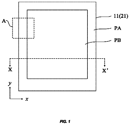
FIG. 1 is a structural diagram of a HSD liquid crystal display panel according to Embodiment 1 of the present disclosure;
FIG. 2 schematically shows waveforms of voltages of driving signals of a data line and several scanning lines of a HSD panel in the prior art;
FIG. 3 schematically shows an equivalent circuit diagram of a sub pixel according to Embodiment 1;
FIG. 4 schematically shows waveforms of voltages of pixel electrodes of sub pixels of a HSD panel in the prior art;
20
FIG. 5 schematically shows waveforms of voltages of pixel electrodes of sub pixels of a HSD panel after being compensated by equivalent capacitances according to Embodiment 1;
FIG. 6 is a structural diagram of a tri-gate liquid crystal display panel according to Embodiment 2 of the present disclosure;
FIG. 7 schematically shows waveforms of voltages of driving signals of a data line and several scanning lines of a tri-gate display panel in the prior art;
30
FIG. 8 schematically shows an equivalent circuit diagram of a sub pixel according to Embodiment 2;
FIG. 9 schematically shows waveforms of voltages of pixel electrodes of sub pixels of a tri-gate display panel in the prior art; and
FIG. 10 schematically shows waveforms of voltages of pixel electrodes of sub pixels of a tri-gate display panel after being compensated by equivalent capacitances according to Embodiment 2.
The present disclosure will be illustrated in more detail hereinafter with reference to the drawings to further clarify the objectives, technical solutions and advantages of the present disclosure. As long as there is no structural conflict, all the technical features mentioned in all the embodiments may be combined together in any manner, and the technical solutions obtained in this manner all fall within the scope of the present disclosure.
Embodiment 1
FIG. 1 is a structural diagram of a HSD liquid crystal display panel according to the present embodiment. As shown in FIG. 1 , the display panel comprises a pixel array formed by a plurality of data lines (such as data lines D 1 , D 2 , D 3 , and D 4 as shown in FIG. 1 ) and a plurality of scanning lines (such as scanning lines G 1 , G 2 , G 3 , and G 4 as shown in FIG. 1 ) that are configured orthogonally to each other, and a plurality of sub pixels P 11 to P 36 that are configured in the array. For the sake of conciseness, it is defined here that a sub pixel Pxy is arranged in row x, and column y. For example, the sub pixel P 12 is arranged in row 1 , and column 2 , and other sub pixels are arranged in the same manner.
The sub pixel P 12 is connected with the scanning line G 1 and the data line D 2 , and a sub pixel P 13 is connected with the scanning line G 2 and the data line D 2 . P 12 and P 13 are arranged at the two sides of the data line D 2 respectively. Similarly, a sub pixel P 22 is connected with the scanning line G 3 and the data line D 2 , and a sub pixel P 23 is connected with the scanning line G 4 and the data line D 2 . Sub pixels P 22 and P 23 are arranged at the two sides of the data line D 2 respectively. Other sub pixels are arranged in a similar manner.
In the prior art, the sub pixels of a HSD liquid crystal display panel would present different degrees of brightness in space during the same frame cycle, and thus bright-dark lines along the vertical direction would occur in the LCD with a HSD pixel array. There are mainly two reasons for this phenomenon.
First, the RC delay of the data line would lead to differences among charge rates of the sub pixels. The waveforms of voltages of driving signals of a data line and several scanning lines during one frame cycle are shown in FIG. 2 . According to the present embodiment, the polarity of the voltage of the driving signal provided by the data line D 2 is reversed periodically. A first time period after polarity reversion is a scanning cycle T 3 , and a second time period is a scanning cycle T 4 . The data line D 2 is used for driving the first sub pixel P 22 and the second sub pixel P 23 . During the scanning cycle T 3 , the first scanning line G 3 is turned on, and the data line D 2 charges the first sub pixel P 22 with a data signal voltage of a positive polarity. Similarly, during the scanning cycle T 4 , the second scanning line G 4 is turned on, and the data line D 2 charges the second sub pixel P 23 with a data signal voltage of a positive polarity. As shown by the dotted line in FIG. 2 , due to the RC delay of the data line D 2 , during a certain time period from the beginning of the scanning cycle T 3 , the driving signal of the data line D 2 cannot reach a preset charge level, which renders that the first sub pixel P 22 is undercharged, and the brightness thereof is relatively low. By contrast, during the scanning cycle T 4 , the driving signal of the data line D 2 has stably reached the preset charge level, so that the second sub pixel P 23 can be charged completely, and the brightness thereof is relatively high.
Second, the reversion driving mode would lead to differences among charge rates of the sub pixels. In general, in a HSD pixel array, a two-horizontal line reversion driving mode, i.e., a two-row reversion driving mode can be used. During two scanning cycles, the polarity of the voltage of the data driving signal is reversed once. That is to say, a reversing cycle of the polarity of the voltage of the driving signal of the data line is equal to two scanning cycles. As shown in FIG. 2 , at an initial moment of the scanning cycle T 3 , the polarity of the voltage of the driving signal of the data line D 2 is reversed, i.e., the driving signal jumps from a low-level signal in the scanning cycle T 2 to a high-level signal in the scanning cycle T 3 . At this time, since the voltage of the driving signal of the data line D 2 should be changed to a rather large extent, the driving signal of the data line D 2 cannot reach the preset charge level during a certain time period from the beginning of the scanning cycle T 3 , which renders that the sub pixel P 22 is undercharged. By contrast, at an initial moment of the scanning cycle T 4 , the polarity of the voltage of the driving signal of the data line D 2 is not reversed. During the scanning cycle T 4 , the driving signal of the data line D 2 can be maintained at the stable preset charge level, and thus the sub pixel P 23 can be charged completely.
On the other hand, since there are parasite capacitors among the sub pixels, a feedthrough voltage would be generated in a pixel electrode of a sub pixel at the moment when the scanning line is turned off, and thus the voltage of the pixel electrode would be reduced. The feedthrough voltage ΔVp can be expressed as: Δ Vp =( Vgh−Vgl )× Cgs /( Cst+Clc+Cgs ), wherein Vgh is a high-level signal of a driving voltage of the scanning line, i.e., a turn-on voltage; Vgl is a low-level signal of the driving voltage of the scanning line, i.e., a turn-off voltage; Cgs is the parasite capacitor; Cst is a storage capacitor; and Clc is a liquid crystal capacitor.
As shown in the equivalent circuit diagram shown of FIG. 3 , an equivalent capacitor is formed by the storage capacitor Cst and the liquid crystal capacitor Clc in parallel connection with each other. In the prior art, an equivalent capacitor C 22 of the sub pixel P 22 is equal to an equivalent capacitor C 23 of the sub pixel P 23 , so that a feedthrough voltage ΔVp 22 of the sub pixel P 22 is equal to a feedthrough voltage ΔVp 23 of the sub pixel P 23 .
Specifically, the waveforms of voltages of pixel electrodes of sub pixels P 22 and P 23 vary as shown in FIG. 4 .
At the initial moment of the scanning cycle T 3 , the scanning line G 3 is turned on, and the driving signal of the data line D 2 cannot reach the preset charge level, which would render that the charge rate of the sub pixel P 22 charged by the data line D 2 is relatively low. At a moment when the scanning cycle T 3 comes to an end, a pixel voltage Vp 22 of the sub pixel P 22 reaches its highest value. After the scanning line G 3 is turned off, a feedthrough voltage ΔVp 22 gradually reduces the pixel voltage Vp 22 to a stable sustaining voltage.
At the initial moment of the scanning cycle T 4 , the scanning line G 4 is turned on, and the driving signal of the data line D 2 can be maintained at the stable preset charge level, so that the charge rate of the sub pixel P 23 charged by the data line D 2 is relatively high. At a moment when the scanning cycle T 4 comes to an end, a pixel voltage Vp 23 of the sub pixel P 23 reaches its highest value, which is higher than the highest value of the pixel voltage Vp 22 of the sub pixel P 22 . After the scanning line G 4 is turned off, a feedthrough voltage ΔVp 23 gradually reduces the pixel voltage Vp 23 to a stable sustaining voltage. Since the voltage of the driving signal of the scanning line G 3 is completely the same as that of the scanning line G 4 , and the equivalent capacitor C 22 of the sub pixel P 22 is equal to the equivalent capacitor C 23 of the sub pixel P 23 , i.e., the feedthrough voltage ΔVp 23 is equal to the feedthrough voltage ΔVp 22 , the stable sustaining voltage Vp 22 of the sub pixel P 22 obtained in the same frame period is lower than the stable sustaining voltage Vp 23 of the sub pixel P 23 , which would result in the brightness presented by the sub pixel P 22 being lower than that of the sub pixel P 23 .
Based on the above analysis, in the present embodiment, the sub pixels are configured with different values of equivalent capacitor, so that different feedthrough voltages can be generated. In this case, the sub pixels, after being charged by the data lines, can obtain the sustaining voltage with the same value. The sub pixels can present a uniform degree of brightness in space, and thus the bright-dark lines along the vertical direction of the HSD liquid crystal display panel can be eliminated.
As shown in FIG. 3 again, the equivalent capacitor C 22 of the sub pixel P 22 can be configured to be larger than the equivalent capacitor C 23 of the sub pixel P 23 , so that the feedthrough voltage ΔVp 22 of the sub pixel P 22 can be less than the feedthrough voltage ΔVp 23 of the sub pixel P 23 . Specifically, it is possible to configure a storage capacitor Cst 22 larger than a storage capacitor Cst 23 , or a liquid crystal capacitor Clc 22 larger than a liquid crystal capacitor Clc 23 . Since the equivalent capacitor is formed by the storage capacitor Cst and the liquid crystal capacitor Clc in parallel connection with each other, it can be readily understood that, it is possible to configure the storage capacitor Cst 22 larger than the storage capacitor Cst 23 , and the liquid crystal capacitor Clc 22 larger than the liquid crystal capacitor Clc 23 at the same time.
In this case, the waveforms of voltages of pixel electrodes of sub pixels P 22 and P 23 vary as shown in FIG. 5 .
At an initial moment of a scanning cycle T 3 , the first scanning line G 3 is turned on, and a driving signal of the data line D 2 cannot reach a preset charge level. In this case, the charge rate of the sub pixel P 22 charged by the data line D 2 is relatively low. At an end of the scanning cycle T 3 , a pixel voltage Vp 22 of the sub pixel P 22 reaches its highest value. After the scanning line G 3 is turned off, a feedthrough voltage ΔVp 22 gradually reduces the pixel voltage Vp 22 to a stable sustaining voltage.
As shown in FIG. 5 , a polarity of the driving signal of the data line D 2 in the scanning cycle T 3 is the same as that in a scanning cycle T 4 . At an initial moment of the scanning cycle T 4 , the second scanning line G 4 is turned on, and the driving signal of the data line D 2 can be maintained at the stable preset charge level. At an end of the scanning cycle T 4 , a pixel voltage Vp 23 of the sub pixel P 23 reaches its highest value, which is higher than the highest value of Vp 22 of the sub pixel P 22 . After the scanning line G 4 is turned off, a feedthrough voltage ΔVp 23 gradually reduces the pixel voltage Vp 23 to a stable sustaining voltage.
Since the voltage of the driving signal provided by the scanning line G 3 is the same as that provided by the scanning line G 4 , and at the moment when the scanning line G 4 is turned off, the voltage of the driving signal thereof can reach the preset level, which is completely the same as that when the scanning line G 3 is turned off, a difference between a turn-on voltage and a turn-off voltage, i.e., (Vgh−Vgl) of the sub pixel P 22 is the same as that of the sub pixel P 23 . As shown in FIG. 5 , according to the present embodiment, the equivalent capacitor C 22 can be configured to be larger than the equivalent capacitor C 23 , so that the feedthrough voltage ΔVp 22 can be less than the feedthrough voltage ΔVp 23 . In this case, the sustaining voltage of the sub pixel P 22 is the same as that of the sub pixel P 23 , and thus the brightness presented by the sub pixel P 22 is the same as that of the sub pixel P 23 .
It should be noted that, the first time period T 3 is equal to the second time period T 4 in duration. That is, the time period during which the scanning line G 3 is turned on is equal to the time period during which the scanning line G 4 is turned on. Moreover, the voltage of the driving signal provided by the scanning line G 3 is the same as that provided by the scanning line G 4 . Therefore, according to the present embodiment, the driving modes of the gate driving chip and the source driving chip as used in the prior art need not to be changed. Hence, the liquid crystal display panel of the present embodiment is compatible with the driving chips in the prior art.
In addition, as mentioned in the above context, at the initial moment of the scanning cycle T 3 , the driving signal of the data line D 2 cannot reach the preset charge level. In this case, the charge rate of the sub pixel P 22 charged by the data line D 2 is relatively low. In fact, compared with the sub pixel P 23 , the equivalent capacitor of the sub pixel P 22 is relatively larger. That is, during the scanning cycle T 3 , the charge load of the sub pixel P 22 charged by the data line D 2 is relatively high, and thus the charge rate thereof is further reduced. For the aforesaid two reasons, the difference between the peak value of the pixel voltage Vp 22 reached therein when the scanning line G 3 is turned off and the peak value of the pixel voltage Vp 23 when the scanning line G 4 is turned off would become larger.
According to the present embodiment, the equivalent capacitor C 22 can be configured to be larger than the equivalent capacitor C 23 , and the difference between the equivalent capacitors C 22 and C 23 can be set to a reasonable value, so that the difference between the peak value of Vp 22 and the peak value of Vp 23 can be compensated. In this manner, the sustaining voltage of the sub pixel P 22 obtained in the same frame period is the same as that of the sub pixel P 23 through the effects of the feedthrough voltages thereof.
It can be readily understood by a person skilled in the art that, the two-row reversion driving mode is applicable for the HSD liquid crystal display panels and traditional liquid crystal display panels. The sub pixels in odd-numbered columns and the sub pixels in even-numbered columns can be configured with different equivalent capacitors, so that different feedthrough voltages can be generated, and thus the different degrees of brightness resulted from the differences among charge rates of sub pixels charged by the data lines can be compensated. In this case, the final charge voltage of the sub pixels in odd-numbered columns is consistent with that of the sub pixels in even-numbered columns, and thus the bright-dark lines along vertical direction can be eliminated.
Embodiment 2
FIG. 6 is a structural diagram of a tri-gate liquid crystal display panel according to the present embodiment. As shown in FIG. 6 , the display panel comprises a pixel array formed by a plurality of data lines (such as data lines D 1 to D 6 as shown in FIG. 6 ) and a plurality of scanning lines (such as scanning lines G 1 to G 6 as shown in FIG. 6 ) that are configured orthogonally to each other, and a plurality of sub pixels P 11 to P 66 that are configured in the array, wherein a red sub pixel (R) P 11 , a green sub pixel (G) P 21 , and a blue sub pixel (B) P 31 form a pixel unit.
In the case that a resolution of the display panel is n×m, a number of scanning lines of the tri-gate liquid crystal display panel is 3m, and a number of data lines thereof is n. By contrast, the number of scanning lines of a traditional display panel is m, and the number of data lines thereof is 3n. In other words, under the same resolution, the number of scanning lines of the tri-gate liquid crystal display panel is increased to three times as that of the traditional display panel, and the number of data lines thereof is reduced to one third of that of the traditional display panel. That is to say, in the tri-gate liquid crystal display panel, relatively more gate driving chips and relatively less source driving chips are used, and thus the manufacturing cost and power consumption thereof can be reduced.
In the prior art, the sub pixels of the tri-gate liquid crystal display panel would present different degrees of brightness in space during the same frame cycle, and thus bright-dark lines along the horizontal direction would occur in the tri-gate pixel array. The reasons for this display defect are stated below.
The waveforms of voltages of driving signals of a data line and several scanning lines in one frame cycle are shown in FIG. 7 . A polarity of a driving signal provided by a data line D 1 is reversed periodically. According to the present embodiment, a first time period after polarity reversion is a scanning cycle T 4 , a second time period is a scanning cycle T 5 , and another second time period is a scanning cycle T 6 . In the present embodiment, the data line D 1 is used for driving a first sub pixel P 41 , a second sub pixel P 51 , and another second sub pixel P 61 . During the scanning cycle T 4 , a first scanning line G 4 is turned on, and the data line D 1 charges the sub pixel P 41 with a data signal voltage of a positive polarity. During the scanning cycle T 5 , a second scanning line G 5 is turned on, and the data line D 1 charges the sub pixel P 51 with a data signal voltage of a positive polarity. Similarly, during the scanning cycle T 6 , another second scanning line G 6 is turned on, and the data line D 1 charges the sub pixel P 61 . The charge time of the sub pixels of the tri-gate display panel reduces two thirds compared with that of the traditional display panel, which would result in the problem of insufficient charge of the sub pixels.
As shown by the dotted line in FIG. 7 , due to the RC delay of the data line D 1 , during a certain time period from the beginning of the scanning cycle T 4 , the driving signal of the data line D 1 cannot reach a preset charge level, which renders that the sub pixel P 41 is undercharged, and the brightness thereof is relatively low. By contrast, during the scanning cycles T 5 and T 6 , the driving signal of the data line D 1 has stably reached the preset charge level, so that the sub pixels P 51 and P 61 can be charged completely, and the brightness thereof is relatively high.
In addition, in the tri-gate pixel array, a three-horizontal line reversion driving mode, i.e., a three-row reversion driving mode can be used. During three scanning cycles, the polarity of the voltage of the data driving signal is reversed once. That is to say, a reversing cycle of the polarity of the voltage of the driving signal of the data line is equal to three scanning cycles. As shown in FIG. 7 , at an initial moment of the scanning cycle T 4 , the polarity of the voltage of the driving signal of the data line D 1 is reversed, i.e., the driving signal jumps from a low-level signal in the scanning cycle T 3 to a high-level signal in the scanning cycle T 4 . At this time, since the voltage of the driving signal of the data line D 1 should be changed to a rather large extent, the driving signal of the data line D 1 cannot reach the preset charge level during a certain time period from the beginning of the scanning cycle T 4 , which renders that the sub pixel P 41 is undercharged. By contrast, at an initial moment of each of the scanning cycles T 5 and T 6 , the polarity of the voltage of the driving signal of the data line D 1 is not reversed. During the scanning cycles T 5 and T 6 , the driving signal of the data line D 1 can be maintained at the stable preset charge level, and thus the sub pixels P 51 and P 61 can be charged completely.
As shown in the equivalent circuit diagram of FIG. 8 , an equivalent capacitor is formed by the storage capacitor Cst and the liquid crystal capacitor Clc in parallel connection with each other. In the prior art, an equivalent capacitor of the sub pixel P 41 is equal to that of the sub pixel P 51 and that of the sub pixel P 61 , so that the feedthrough voltage ΔVp 41 of the sub pixel P 41 is equal to the feedthrough voltage ΔVp 51 of the sub pixel P 51 , and also equal to the feedthrough voltage ΔVp 61 of the sub pixel P 61 .
Similar to embodiment 1, affected by the feedthrough voltages caused by the parasite capacitors thereof, the waveforms of voltages of pixel electrodes of the sub pixels P 41 , P 51 and P 61 vary as shown in FIG. 9 .
At the initial moment of the scanning cycle T 4 , the scanning line G 4 is turned on, and the driving signal of the data line D 1 cannot reach the preset charge level, which would render that the charge rate of the sub pixel P 41 charged by the data line D 1 is relatively low. At a moment when the scanning cycle T 4 comes to an end, a pixel voltage Vp 41 of the sub pixel P 41 reaches its highest value. After the scanning line G 4 is turned off, a feedthrough voltage ΔVp 41 gradually reduces the pixel voltage Vp 41 to a stable sustaining voltage.
At the initial moment of the scanning cycle T 5 , the scanning line G 5 is turned on, and the driving signal of the data line D 1 can be maintained at the stable preset charge level, so that the charge rate of the sub pixel P 51 charged by the data line D 1 is relatively high. At a moment when the scanning cycle T 5 comes to an end, a pixel voltage Vp 51 of the sub pixel P 51 reaches its highest value, which is higher than the highest value of the pixel voltage Vp 41 of the sub pixel P 41 . After the scanning line G 5 is turned off, a feedthrough voltage ΔVp 51 gradually reduces the pixel voltage Vp 51 to a stable sustaining voltage.
Similarly, at the initial moment of the scanning cycle T 6 , the scanning line G 6 is turned on, and the charge rate of the sub pixel P 61 charged by the data line D 1 is relatively high. After the scanning line G 6 is turned off, a feedthrough voltage ΔVp 61 gradually reduces the pixel voltage Vp 61 to a stable sustaining voltage.
Since the voltage of the driving signal of the scanning line G 4 is completely the same as those of the scanning lines G 5 and G 6 , and the equivalent capacitor C 41 is equal to the equivalent capacitor C 51 and the equivalent capacitor C 61 , i.e., the feedthrough voltages ΔVp 41 , ΔVp 51 and ΔVp 61 are equal to one another, the stable pixel voltage Vp 41 of the sub pixel P 41 obtained in the same frame period is lower than those of the sub pixels P 51 and P 61 , which would result in that the brightness presented by the sub pixel P 41 is relatively low while the brightness presented by the sub pixels P 51 and P 61 is relatively high.
Based on the above analysis, in the present embodiment, the sub pixels are configured with different values of equivalent capacitor, so that different feedthrough voltages can be generated. In this case, the sub pixels, after being charged by the data line, can obtain the sustaining voltage with the same value.
As shown in FIG. 8 again, the equivalent capacitor C 41 of the sub pixel P 41 can be configured to be larger than that of the second sub pixel P 51 and another second sub pixel P 61 , i.e., C 41 >C 51 =C 61 , so that the feedthrough voltages ΔVp 41 <ΔVp 51 =A Vp 61 can be generated. Specifically, it is possible to configure the storage capacitors thereof Cst 41 >Cst 51 =Cst 61 , or the liquid crystal capacitors thereof Clc 41 >Clc 51 =Clc 61 . Since the equivalent capacitor is formed by the storage capacitor Cst and the liquid crystal capacitor Clc in parallel connection with each other, it can be readily understood that, it is possible to configure the storage capacitors thereof Cst 41 >Cst 51 =Cst 61 , and the liquid crystal capacitors thereof Clc 41 >Clc 51 =Clc 61 at the same time.
In this case, the waveforms of voltages of pixel electrodes of the sub pixels P 41 , P 51 , and P 61 vary as shown in FIG. 10 .
At an initial moment of a scanning cycle T 4 , a driving signal of the data line D 1 cannot reach a preset charge level. In this case, the charge rate of the sub pixel P 41 charged by the data line D 1 is relatively low. At an end of the scanning cycle T 4 , a pixel voltage Vp 41 of the sub pixel P 41 reaches its highest value. After the scanning line G 4 is turned off, a feedthrough voltage ΔVp 41 gradually reduces the pixel voltage Vp 41 to a stable sustaining voltage.
As shown in FIG. 10 , a polarity of the driving signal of the data line D 1 in the scanning cycle T 4 is the same as that in a scanning cycle T 5 . At an initial moment of the scanning cycle T 5 , the driving signal of the data line D 1 can be maintained at the stable preset charge level. At an end of the scanning cycle T 5 , a pixel voltage Vp 51 of the sub pixel P 51 reaches its highest value, which is higher than the highest value of Vp 41 of the sub pixel P 41 . After the scanning line G 5 is turned off, a feedthrough voltage ΔVp 51 gradually reduces the pixel voltage Vp 51 to a stable sustaining voltage.
Since the voltage of the driving signal provided by the scanning line G 4 is the same as those provided by the scanning lines G 5 and G 6 , and at the moment when the scanning lines G 5 and G 6 are turned off, the voltage of the driving signal thereof can reach the preset level, which is completely the same as that when the scanning line G 4 is turned off, a difference between a turn-on voltage and a turn-off voltage, i.e., (Vgh−Vgl) of the sub pixel P 41 is the same as those of the sub pixels P 51 and P 61 . As shown in FIG. 8 , according to the present embodiment, the equivalent capacitors thereof C 41 >C 51 =C 61 can be configured, so that the feedthrough voltages thereof ΔVp 41 <ΔVp 51 =ΔVp 61 can be generated. In this case, the sustaining voltage of the sub pixel P 41 is the same as those of the sub pixels P 51 and P 61 , and thus the brightness presented by the sub pixel P 41 is the same as those of the sub pixels P 51 and P 61 .
It should be noted that, the scanning cycles T 4 , T 5 , and T 6 are equal to one another in duration. That is, the time period during which the scanning line G 4 is turned on is equal to the time period during which the scanning line G 5 is turned on, and also equal to the time period during which the scanning line G 6 is turned on. Moreover, the voltage of the driving signal provided by the scanning line G 4 is the same as those provided by the scanning lines G 5 and G 6 . Therefore, according to the present embodiment, the driving modes of the gate driving chip and the source driving chip of a tri-gate liquid crystal display panel as used in the prior art need not to be changed. Hence, the liquid crystal display panel of the present embodiment is compatible with the driving chips in the prior art.
Similar to embodiment 1, since the value of the equivalent capacitor C 41 is increased, the charge load of the sub pixel P 41 charged by the data line D 1 is relatively high, and thus the charge rate thereof is further reduced. Consequently, the differences among the peak values of the pixel voltages Vp 41 , Vp 51 , and Vp 61 reached therein when the corresponding scanning line is turned off would become larger. The equivalent capacitors C 41 , C 51 , and C 61 can be configured with different values, so that the sustaining voltage of the sub pixel P 41 is equal to those of the sub pixels P 51 and P 61 through the effects of the feedthrough voltages.
In addition, during the driving procedure of the tri-gate liquid crystal display panel, the RC delay effect of the data line would become more serious. Different from the driving signal of the data line D 1 as shown in FIG. 9 , the voltage of the driving signal of the data line D 1 cannot reach the preset charge level during both the scanning cycles T 4 and T 5 . In this case, the sub pixels P 41 and P 51 are both undercharged, which would result in the peak values of the pixel voltages Vp 41 and Vp 51 being lower than that of the pixel voltage Vp 61 . Consequently, the brightness presented by the sub pixels P 41 and P 51 is relatively low, while the brightness presented by the sub pixel P 61 is relatively high. Similarly, the equivalent capacitors C 41 , C 51 , and C 61 can be configured with different values, so that the sustaining voltage of the sub pixels P 41 and P 51 can be equal to that of the sub pixel P 61 through the effects of the feedthrough voltages.
It can be readily understood by a person skilled in the art that, as to the tri-gate liquid crystal display panel, the equivalent capacitor of the sub pixels in the 3k+1 and 3k+2 rows can be configured to be different from that of the sub pixels in the 3k rows (k is an integer and equal to or larger than 0), so that different feedthrough voltages can be generated. In this case, the sub pixels in different rows can obtain the same sustaining voltage after being charged by respective data lines, and the bright-dark lines along the horizontal direction can be eliminated.
In addition, the three-row reversion driving mode is applicable for the HSD liquid crystal display panels of embodiment 1 and traditional liquid crystal display panels. Under the reversion driving mode, the equivalent capacitor of the sub pixels in the 3k+1 and 3k+2 rows can be configured to be different from that of the sub pixels in the 3k rows, so that the difference among charge rates of the sub pixels charged by the data line can be compensated, and the display defect of uneven brightness can be eliminated.
The above embodiments are described only for better understanding, rather than restricting, the present disclosure. Any person skilled in the art can make amendments to the implementing forms or details without departing from the spirit and scope of the present disclosure. The protection scope of the present disclosure shall be determined by the scope as defined in the claims.
About 7,282 words. The USPTO PDF has it with every drawing.
Fees are due 3.5, 7.5 and 11.5 years after grant. This patent expired on April 24, 2026, so the fee marked "not paid" was the one that went unpaid.
LIQUID CRYSTAL DISPLAY PANEL
Filed Dec 2014 · published Dec 2016Liquid crystal display panel
Filed Dec 2014 · granted Apr 2018Earlier publications, parents and continuations. None of them can still be enforced, or this patent would not be listed.
Prior art cited by the examiner or applicant. Useful when you check your own idea for novelty.
Everything on this page comes from the documents linked above.