Background of the invention
1. Field of the invention
The present invention relates to a semiconductor light-emitting element such as a light-emitting diode (LED) and a semiconductor light-emitting device including a plurality of semiconductor light-emitting elements.
2. Description of the related art
Semiconductor light-emitting elements are generally fabricated by growing a semiconductor structure layer having an n-type semiconductor layer, a light-emitting layer and a p-type semiconductor layer on a growth substrate, and forming an n-electrode and a p-electrode that apply voltage to the n-type semiconductor layer and the p-type semiconductor layer, respectively. Furthermore, semiconductor light-emitting elements with improved heat dissipation performance are known. The semiconductor light-emitting elements are formed by joining a semiconductor structure layer formed on a growth substrate to a support substrate other than the growth substrate, and then removing the growth substrate. Semiconductor light-emitting devices are fabricated by fixing a plurality of semiconductor light-emitting elements on a mounting substrate, further forming a phosphor layer for wavelength conversion, and then packaging an entire body by a resin and the like. Japanese Patent Application Laid-Open No. 2014-195123 discloses an AC semiconductor light-emitting element having an array of light-emitting cells connected in series.
Summary of the invention
For example, in the field of lighting apparatuses such as vehicle lamps, it is sometimes required to arrange light distribution so that some irradiated area is brighter than other areas. To meet such a requirement, a light source is configured so that the irradiated area includes a high-luminance region and a low-luminance region for example. In this case, in consideration of providing a vehicle driver with comfortable visibility, it is preferable to gradually vary the luminance on a boundary between the high-luminance region and the low-luminance region. That is, it is preferable to form a luminance gradation region (inclination region) between the high-luminance region and the low-luminance region. On the other hand, in view of ensuring visibility of the entire irradiated area, it is preferable to impart a high luminance to the entire irradiation area.
The present invention has been made in view of the above-described points, and it is therefore an object of the present invention to provide a semiconductor light-emitting element and a semiconductor light-emitting device having high light-extraction efficiency and capable of forming a luminance gradation.
A semiconductor light-emitting element according to the present invention includes: a semiconductor structure layer including a first semiconductor layer having a first conductivity type, a light-emitting layer and a second semiconductor layer having a second conductivity type opposite to the first conductivity type being laminated in sequence; a first electrode including a first electrode layer formed on the first semiconductor layer and a first contact electrode connected to the first electrode layer at a position displaced from a center of the first electrode layer in an intra-layer direction of the first electrode layer; and a second electrode extending through the first electrode layer, the first semiconductor layer, and the light-emitting layer and being connected to the second semiconductor layer.
A semiconductor light-emitting device according to the present invention includes: a substrate; and a plurality of semiconductor light-emitting elements arrayed in a matrix form on the substrate, the semiconductor light-emitting elements each having a semiconductor structure layer configured to include a first semiconductor layer having a first conductivity type, a light-emitting layer and a second semiconductor layer having a second conductivity type opposite to the first conductivity type being laminated in sequence, and first and second electrodes connected to the first and second semiconductor layers, wherein among the plurality of semiconductor light-emitting elements, the first electrode in at least one semiconductor light-emitting element at an end portion includes: a first electrode layer formed on the first semiconductor layer; and a first contact electrode connected to the first electrode layer at a position displaced from a center of the first electrode layer in an intra-layer direction of the first electrode layer, and the second electrode in the at least one semiconductor light-emitting element includes: a second electrode layer provided between the substrate and the first electrode layer; and a plurality of via-electrodes extending from the second electrode layer and through the first electrode layer, the first semiconductor layer, and the light-emitting layer and being connected to the second semiconductor layer.
Brief description of the drawings
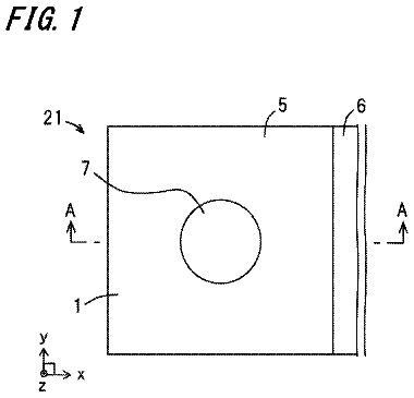
FIG. 1A is a cross-sectional view of a semiconductor light-emitting element according to a first embodiment, and FIGS. 1B and 1C are schematic views illustrating an upper surface of the semiconductor light-emitting element of the first embodiment;
FIG. 2A is a cross-sectional view illustrating a semiconductor light-emitting element according to a second embodiment, and FIG. 2B is a schematic top view illustrating the semiconductor light-emitting element according to the second embodiment;
FIG. 3A is a schematic view illustrating an upper surface of a semiconductor light-emitting device according to a third embodiment, and FIG. 3B is a fragmentary cross-sectional view illustrating the semiconductor light-emitting device according to the third embodiment;
FIG. 4A is a schematic view illustrating an upper surface of a semiconductor light-emitting device according to a first modification of the third embodiment, and FIG. 4B is a fragmentary cross-sectional view illustrating the semiconductor light-emitting device according to the first modification of the third embodiment;
FIG. 5A is a schematic view illustrating an upper surface of a semiconductor light-emitting device according to a second modification of the third embodiment, and FIG. 5B is a schematic view illustrating an upper surface of a semiconductor light-emitting device according to a third modification of the third embodiment; and
FIGS. 6A and 6B are schematic views illustrating an upper surface of a semiconductor light-emitting device according to a fourth embodiment.
Detailed description of the invention
Hereinbelow, embodiments of the present invention will be described in detail.
[First Embodiment]
FIG. 1A is a cross-sectional view of a semiconductor light-emitting element (hereinafter simply referred to as a light-emitting element) 10 according to a first embodiment. The light-emitting element 10 includes a semiconductor structure layer SCL, a p-electrode (first electrode) PE, and an n-electrode (second electrode) NE. The semiconductor structure layer SCL includes a p-type semiconductor layer (first semiconductor layer having a first conductivity type) 11 , a light-emitting layer 12 , and an n-type semiconductor layer (second semiconductor layer having a second conductivity type opposite to the first conductivity type) 13 . For example, the semiconductor structure layer SCL is configured to include the p-type semiconductor layer 11 having a composition of Al.sub.xIn.sub.yGa.sub.1−x−yN (0≤x≤1, 0≤y≤1), the light-emitting layer 12 , and the n-type semiconductor layer 13 laminated in sequence on the mounting substrate SB (hereinafter simply referred to as a substrate). The surface of the n-type semiconductor layer 13 functions as a light extraction surface.
The light-emitting element 10 also includes a p-side pad terminal (first terminal) PP and an n-side pad terminal (second terminal) NP provided on the substrate SB to supply electric power to the p-electrode PE and the n-electrode NE, respectively. The p-side pad terminal PP and the n-side pad terminal NP are connected to an external power supply (not illustrated) through a bonding wire (not illustrated), for example. The p-electrode PE and the n-electrode NE are connected to the p-type and n-type semiconductor layers 11 and 13 , respectively.
The p-electrode PE includes a p-electrode layer (first electrode layer) PEL formed on the p-type semiconductor layer 11 so as to coat the surface of the p-type semiconductor layer 11 . The p-electrode PE includes a p-side contact electrode (first contact electrode) PCE connected to the p-electrode layer PEL between the substrate SB and the semiconductor structure layer SCL. On the substrate SB, a p-side wiring PW wired from the p-side pad terminal PP to the p-electrode layer PEL is provided. The p-side wiring PW is wired from the p-side pad terminal PP to the p-electrode layer PEL through the p-side contact electrode PCE.
The n-electrode NE includes a plurality of via-electrodes VE extending through the p-type semiconductor layer 11 and the light-emitting layer 12 between the substrate SB and the semiconductor structure layer SCL and being connected to the n-type semiconductor layer 13 . The n-electrode NE also includes an n-electrode layer (second electrode layer) NEL formed between the substrate SB and the p-electrode layer PEL and connected to the plurality of via-electrodes VE. That is, the n-electrode NE extends through the p-electrode layer PEL, the p-type semiconductor layer 11 , and the light-emitting layer 12 and is connected to the n-type semiconductor layer 13 . The n-electrode layer NEL is connected to the n-side pad terminal NP.
In the present embodiment, the p-side wiring PW is formed on the substrate SB, and an insulating layer ISL is formed on the p-side wiring PW. On the insulating layer ISL, the n-electrode layer NEL is formed. On the n-electrode layer NEL, an insulating film ISF is formed. On the insulating film ISF, the p-electrode layer PEL is formed. The p-side contact electrode PCE extends from the p-electrode layer PEL and through the insulating film ISF, the n-electrode layer NEL, and the insulating layer ISL, and is connected to the p-side wiring PW.
The p-side wiring PW and the n-electrode layer NEL are three-dimensionally formed so as to be in different hierarchies across the insulating layer ISL between the substrate SB and the semiconductor structure layer SCL. The n-electrode layer NEL and the p-electrode layer PEL are three-dimensionally formed so as to be in different hierarchies across the insulating film ISF between the substrate SB and the semiconductor structure layer SCL. That is, the n-electrode layer NEL is formed on the p-electrode layer PEL through the insulating film ISF. The insulating layer ISL and the insulating film ISF are comprised of an insulating material such as SiO.sub.2, for example.
The p-electrode layer PEL is formed of a multilayered metal layer including a reflective metal layer (not illustrated) and a cap layer (not illustrated) laminated on the p-type semiconductor layer 11 , for example. The reflective metal layer is comprised of, for example, a metal material such as Ag, Pt, Ni, Al, or Pd, or an alloy containing the same. The cap layer is formed by using a metal material less likely to cause migration, such as Ti, W, Pt, Pd, Mo, Ru, Ir, or Au, for example. A metal oxide film, such as ITO or IZO, may be formed between the p-type semiconductor layer 11 and the reflective metal layer to enhance optical reflexibility. The via-electrodes VE are formed by using a metal material such as Ti, Al, Pt, or Au. For example, the n-electrode layer NEL is formed by using a metal material such as Ti, Pt, or Au.
As illustrated in FIG. 1A , the p-side contact electrode PCE is connected to the p-electrode layer PEL at a position displaced (biased) from a center (central point) CP of the p-electrode layer PEL in an intra-layer direction of the p-electrode layer PEL. Therefore, the p-side contact electrode PCE is formed at a displaced position on the semiconductor structure layer SCL. The p-side wiring PW is connected to the p-electrode layer PEL at a displaced position in the intra-layer direction of the semiconductor structure layer SCL. For example, the p-side contact electrode PCE is preferably formed at a position within a distance of ⅓, preferably within a distance of ¼, of the length of the semiconductor structure layer SCL in a displacement direction from an end portion of the semiconductor structure layer SCL in the displacement direction.
In the present embodiment, the p-side contact electrode PCE is formed at a position displaced in a direction away from the p-side pad terminal PP in the intra-layer direction of the p-electrode layer PEL. The n-side pad terminal NP is formed at a position facing the p-side pad terminal PP across the semiconductor structure layer SCL. Therefore, the p-side contact electrode PCE is formed at a displaced position in a direction approaching the n-side pad terminal NP in the intra-layer direction of the semiconductor structure layer SCL.
FIGS. 1B and 1C are schematic views illustrating the upper surface of the light-emitting element 10 . FIG. 1A is a cross-sectional view taken along V-V line in FIGS. 1B and 1C . FIG. 1B schematically illustrates not only the upper surface of the light-emitting element 10 , but also formation regions of the p-electrode layer PEL, the p-side contact electrode PCE, the p-side wiring PW, and the via-electrodes VE. For the clarity of the drawing, hatching is applied to the formation regions of the p-electrode layer PEL and the p-side contact electrode PCE, and the formation regions of the p-side wiring PW and the via-electrodes VE in the lower layer of the semiconductor structure layer SCL are illustrated with broken lines.
First, in the present embodiment, the semiconductor structure layer SCL has a rectangular shape as viewed from a direction perpendicular to the semiconductor structure layer SCL. The p-side pad terminal PP and the n-side pad terminal NP face each other across the semiconductor structure layer SCL in a longitudinal direction of the semiconductor structure layer SCL. Four via-electrodes VE are formed at regular intervals along the longitudinal direction of the semiconductor structure layer SCL. The p-side contact electrode PCE is formed between two via-electrodes VE on the n-side pad terminal NP side, among the four via-electrodes VE.
As illustrated in FIG. 1B , the p-electrode layer PEL is formed so as to cover almost the entire p-type semiconductor layer 11 except the formation region of the via-electrodes VE. Therefore, a current supplied from the p-side pad terminal PP and through the p-side wiring PW and the p-side contact electrode PCE to the p-electrode layer PEL diffuses to the entire p-electrode layer PEL, and is then injected into the p-type semiconductor layer 11 . That is, the p-electrode layer PEL functions as a current diffusion layer (first current diffusion layer).
Next, the n-electrode layer NEL and the via-electrodes VE will be described with reference to FIG. 1C . In FIG. 1C , for clarity of the drawings, hatching is applied to the formation regions of the n-electrode layer NEL and the via-electrodes VE, and the formation region of the p-side contact electrode PCE is illustrated with a broken line. First, the n-electrode layer NEL is formed on almost an entire region between the semiconductor structure layer SCL and the substrate SB except the formation region of the p-side contact electrode PCE. In the present embodiment, four via-electrodes VE are uniformly distributed in the intra-layer direction of the semiconductor structure layer SCL. Therefore, a current passing through the n-type semiconductor layer 13 diffuses in the n-electrode layer NEL through all the via-electrodes VE and then flows toward the n-side pad terminal NP. That is, the n-electrode layer NEL functions as a current diffusion layer (second current diffusion layer).
Next, the p-side contact electrode PCE will be described with reference to FIG. 1B again. The p-side contact electrode PCE is formed at a position displaced from the center CP of the p-electrode layer PEL in the intra-layer direction of the p-electrode layer PEL. Therefore, a point of injecting the current into the p-electrode layer PEL is formed at a displaced position in the intra-layer direction of the semiconductor structure layer SCL (p-type semiconductor layer 11 ). This hinders uniform injection of the current into the intra-layer direction of the light-emitting layer 12 . Therefore, the light emitted from the light-emitting layer 12 is different in amount in the surface of the light-emitting layer 12 .
Specifically, light with relatively high luminance is emitted from a region of the light-emitting layer 12 in the vicinity of the p-side contact electrode PCE (on the left side of the center CP in the drawing) in the intra-layer direction of the semiconductor structure layer SCL. Meanwhile, light with relatively low luminance is emitted from a region of the light-emitting layer 12 away from the p-side contact electrode PCE (on the right side of the center CP in the drawing). Therefore, a relatively bright region (high-luminance region) H 1 and a relatively dark region (low-luminance region) L 0 are formed in the light-emitting element 10 . Since the light is uninterruptedly emitted from the light-emitting layer 12 , the luminance of the light emitted from the light-emitting layer 12 continuously changes. This makes it possible to intentionally form a luminance inclination (gradation) on the light extraction surface (the surface of the n-type semiconductor layer 13 in the present embodiment).
Since both the p-electrode PE and the n-electrode NE are formed between the substrate SB and the semiconductor structure layer SCL (on the p-type semiconductor layer 11 side in the semiconductor structure layer SCL), a metal material which can intercept passage of light is not formed on the surface of the n-type semiconductor layer 13 . Therefore, light can be extracted from the entire surface of the n-type semiconductor layer 13 that serves as a light extraction surface. This makes it possible to suppress formation of a dark part in an irradiation image.
In the present embodiment, the semiconductor structure layer SCL has a rectangular shape as viewed from the direction perpendicular to the semiconductor structure layer SCL. As illustrated in FIGS. 1B and 1C , the p-side contact electrode PCE is formed at a position displaced from the center of the p-electrode layer PEL along the longitudinal direction of the semiconductor structure layer SCL. Therefore, a large luminance inclination is formed in the longitudinal direction of the semiconductor structure layer SCL.
Moreover, in the present embodiment, the n-electrode NE is comprised of an n-electrode layer NEL and via-electrodes VE. The n-electrode NE is pulled out from a position (vicinity of high-luminance region HI) of the semiconductor structure layer SCL (n-type semiconductor layer 13 ) displaced in a direction identical to the displacement direction of the p-side contact electrode PCE. That is, the n-electrode layer NEL is pulled out so as to form a current path in a direction toward the p-side contact electrode PCE from the center CP of the n-electrode layer NEL in the intra-layer direction of the n-electrode layer NEL. Therefore, the current tends to concentrate in the region of the light-emitting layer 12 in the vicinity of the p-side contact electrode PCE. As a result, a larger luminance gradation is formed.
In the present embodiment, it has been described that the p-side and n-side pad terminals PP and NP are formed on the substrate SB so that they face each other across the semiconductor structure layer SCL. However, the p-side and n-side pad terminals PP and NP may be formed at other positions.
Although it has been described that the n-electrode NE includes the n-electrode layer NEL and the via-electrodes VE, the n-electrode NE is not limited to the configuration of including the n-electrode layer NEL and the via-electrodes VE so long as the n-electrode NE extends through the p-electrode layer PEL, the p-type semiconductor layer 11 , and the light-emitting layer 12 between the substrate SB and the semiconductor structure layer SCL, and is connected to the n-type semiconductor layer 13 . This makes it possible to supply the amount of current injected into the light-emitting layer 12 in a biased manner, so that a fixed luminance inclination can be formed.
Although it has been described that the semiconductor structure layer SCL has a rectangular plane shape, the plane shape of the semiconductor structure layer SCL is not limited to the rectangular plane shape. Although it has been described that the p-side pad terminal PP and the p-side contact electrode PCE (p-electrode PE) are connected through the p-side wiring PW, the p-electrode PE and the p-side pad terminal PP may be connected in other forms. Although it has been described that the n-side pad terminal NP is directly connected to the n-electrode layer NEL (n-electrode NE), the n-side pad terminal NP and the n-electrode NE may be connected in other forms.
As illustrated in FIG. 1A , forming an uneven structure on the surface (light extraction surface) of the n-type semiconductor layer 13 enables larger amount of light to pass through the uneven structure. As a result, the light extraction efficiency can be improved. Although it has been described that the first and second semiconductor layers are a p-type semiconductor layer and an n-type semiconductor layer, respectively, in the present embodiment, the conductivity type of the first and second semiconductor layers may be reversed. That is, the first semiconductor layer may have an n-type conductivity type, and the second semiconductor layer may have a p-type conductivity type.
In the present embodiment, the p-electrode PE includes a p-electrode layer PEL and a p-side contact electrode PCE connected to a displaced position of the p-electrode layer PEL. The n-electrode NE extends through the p-electrode layer PEL, the p-type semiconductor layer 11 , and the light-emitting layer 12 between the substrate SB and the semiconductor structure layer SCL, and is connected to the n-type semiconductor layer 13 . This makes it possible to secure current injection into the entire light-emitting layer 12 , while intentionally supplying the current injection into the light-emitting layer 12 in a biased manner. Therefore, the light-emitting element 10 having a luminance distribution (gradation) can be obtained. As a result, irradiation light with a large luminance gradation can be obtained.
[Second Embodiment]
FIG. 2A is a cross-sectional view illustrating a configuration of a semiconductor light-emitting element (hereinafter simply referred to as a light-emitting element) 20 according to a second embodiment. FIG. 2B is a schematic view illustrating an upper surface of the light-emitting element 20 . FIG. 2A is a cross-sectional view taken along W-W line of FIG. 2B . The light-emitting element 20 has the same configuration as the light-emitting element 10 except for the configuration of the n-electrode NE and the presence of a back surface terminal BT.
In the present embodiment, an n-electrode NE includes not only via-electrodes VE and an n-electrode layer (second electrode layer) NEL, but also an n-side contact electrode (second contact electrode) NCE connected to the n-electrode layer NEL at a position displaced to a p-side contact electrode PCE of the n-electrode layer NEL. More specifically, the n-electrode NE includes: the n-electrode NEL formed on the p-electrode layer PEL through an insulating film ISF; a plurality of via-electrodes VE extending from the n-electrode layer NEL and through the p-electrode layer PEL, a p-type semiconductor layer 11 , and a light-emitting layer 12 and being connected to an n-type semiconductor layer 13 ; and the n-side contact electrode NCE connected to the n-electrode layer NEL at a position displaced (biased) in a direction toward the p-side contact electrode PCE from the center CP of the n-electrode layer NEL in the intra-layer direction of the n-electrode layer NEL. In the description of the present embodiment, the center CP of the p-electrode layer PEL is identical to the center CP of the n-electrode layer NEL as viewed from a direction perpendicular to the semiconductor structure layer SCL.
In the present embodiment, the n-side contact electrode NCE extends from the n-electrode layer NEL and through the insulating layer ISL and is connected to the substrate SB. On the back surface (surface without the insulating layer ISL formed thereon) of the substrate SB, a back surface terminal BT is formed. In the present embodiment, the substrate SB is formed from a conductive substrate such as Si. That is, the n-electrode NE is electrically connected to the back surface terminal BT through the substrate SB. Although the n-side pad terminal NP is used as a feed terminal to the n-type semiconductor layer 13 in the first embodiment, the back surface terminal BT functions as a feed terminal to the n-type semiconductor layer 13 in the present embodiment.
As illustrated in FIG. 2B , the light-emitting element 20 includes p-side and n-side contact electrodes PCE and NCE which are displaced in an identical direction from the center CP of the semiconductor structure layer SCL in the intra-layer direction of the semiconductor structure layer SCL. The p-electrode layer PEL and n-electrode layer NEL which function as current diffusion layers are connected to the p-side and n-side contact electrodes PCE and NCE, respectively. This makes it possible to secure current injection into the entire light-emitting layer 12 , while forming a large luminance gradation in the irradiation area.
The semiconductor structure layer SCL has a rectangular shape as viewed in the direction perpendicular to the semiconductor structure layer SCL. The p-side and n-side contact electrodes PCE and NCE are each formed at positions displaced from the centers CP of the p-electrode layer PEL and the n-electrode layer NEL along the long-side direction of the semiconductor structure layer SCL. Therefore, a large luminance gradation can be formed.
[Third Embodiment]
FIG. 3A is a schematic view illustrating an upper surface of a semiconductor light-emitting device (hereinafter simply referred to as a light-emitting device) 30 according to a third embodiment. The light-emitting device 30 includes a plurality of semiconductor light-emitting elements (hereinafter simply referred to as light-emitting elements) 40 arrayed in a matrix form (in n rows and m columns, 1≤n, 1≤m) on the substrate SB. In the present embodiment, four light-emitting elements 40 are arranged in a row between the p-side and n-side pad terminals PP and NP. In the following description, among the four light-emitting elements 40 , a light-emitting element 40 closest to the p-side pad terminal PP (end portion) is referred to as a light-emitting element 40 A, and a light-emitting element 40 adjacent to the light-emitting element 40 A is referred to as a light-emitting element 40 B.
FIG. 3B is a cross-sectional view of the light-emitting device 30 . FIG. 3B is a cross-sectional view taken along X-X line of FIG. 3A . As illustrated in FIG. 3B , like the light-emitting element 10 , the light-emitting element 40 A in an end portion includes: a p-electrode (first electrode) PE comprised of a p-electrode layer (first electrode layer) PEL and a p-side contact electrode (first contact electrode) PCE; and an n-electrode (second electrode) NE comprised of an n-electrode layer (second electrode layer) NEL and via-electrodes VE. Like the light-emitting element 10 , the p-electrode PE of the light-emitting element 40 A is connected to the p-side pad terminal PP through a p-side wiring PW provided on the substrate SB.
The n-electrode NE of the light-emitting element 40 A is connected to a p-electrode PE of the adjacent light-emitting element 40 B. Specifically, the n-electrode layer NEL of the light-emitting element 40 A extends between the light-emitting element 40 B and the substrate SB. The p-electrode PE of the light-emitting element 40 B includes a p-electrode layer PEL similar to that of the light-emitting element 10 , and a p-side contact electrode PCE connected from the p-electrode layer PEL to the n-electrode layer NEL of the light-emitting element 40 A. More specifically, the adjacent light-emitting elements 40 A and 40 B are connected in series. The light-emitting elements 40 other than the light-emitting elements 40 A and 40 B have the same configuration as that of the light-emitting element 40 B.
Similarly, four light-emitting elements 40 are connected to adjacent light-emitting elements 40 as in the case of the light-emitting elements 40 A and 40 B. As illustrated in FIG. 3A , the n-electrode layer NEL in the light-emitting element 40 closest to the n-side pad terminal NP is connected to the n-side pad terminal NP. That is, the light-emitting device 30 is configured so that the plurality of light-emitting elements 40 are connected in series. Therefore, when voltage is applied between the p-side pad terminal PP and the n-side pad terminal NP, all the light-emitting elements 40 perform lighting operation at the same time.
In the present embodiment, the light-emitting element 40 A in the end portion has the p-side contact electrode PCE. Therefore, a luminance gradation can be formed in an end area of the light-emitting region (element region). For example, when the light-emitting device 30 is used as lighting, a gentle luminance gradation is formed at an outer edge of the irradiation area.
Moreover, in the present embodiment, the p-side contact electrode PCE of the light-emitting element 40 A is formed at a position displaced toward the adjacent light-emitting element 40 B from the center of the p-electrode layer PEL. Therefore, it becomes possible to form a luminance gradation with the luminance gradually decreasing toward the outer edge of the light-emitting region. For example, when the light-emitting device 30 is used as a vehicle headlight, the center of an irradiation area (for example, a portion of illuminating the front side of the vehicle within a present lane) is required to be high in luminance, while the luminance requirements are less severe (low luminance is acceptable) with respect to the outer edge of the irradiation area (for example, a portion of illumination side roads and road signs). In such an application, the light-emitting device 30 is preferable.
The light-emitting element 40 A has a rectangular shape as viewed from a direction perpendicular to the semiconductor structure layer SCL, with the long-side of the rectangular shape being in the direction toward the adjacent light-emitting element 40 B. In the light-emitting element 40 A, the p-side contact electrode PCE is formed at a position displaced from the center of the p-electrode layer PEL along the long-side direction of the semiconductor structure layer SCL. Therefore, a large luminance gradation is formed in the light-emitting element 40 A. As a result, it becomes possible to form extraction light with the luminance decreasing largely and smoothly toward the outer edge.
Since the p-side contact electrode PCE of the light-emitting element 40 A is formed at a position displaced toward the adjacent light-emitting element 40 B, a high-luminance region H 1 (see FIG. 1B ) is formed on the light-emitting element 40 B side of the light-emitting element 40 A. In this case, light tends to pass through a region between the light-emitting elements 40 A and 40 B. Specifically, while light is not emitted from the region between the element 40 A and 40 B, most of the light emitted from the light-emitting element 40 A tends to pass through the inter-element region in the present embodiment. Therefore, when all the light-emitting elements 40 are lit, formation of a dark part (dark line) corresponding to an inter-element region is suppressed. In the present embodiment, since the n-electrode layer NEL is pulled out toward the light-emitting element 40 B which is adjacent in a direction displaced from the central point CP of the p-side contact electrode PCE, formation of the dark part is further suppressed.
In the present embodiment, it has been described that four light-emitting elements 40 are arrayed in a row. However, the number of the light-emitting elements in a row, and the number of rows and columns are not limited thereto. For example, the light-emitting elements may be arrayed in two or more rows. In that case, the light-emitting elements in the end portions may each include a p-side contact electrode PCE placed at a displaced position, or one of the light-emitting elements in the end portions may include the p-side contact electrode PCE. More specifically, among the plurality of light-emitting elements arrayed in a matrix form, at least one light-emitting element in the end portion may include the p-electrode PE and the n-electrode NE similar to those of the light-emitting element 10 .
In the present embodiment, it has been described that the light-emitting element 40 A has a rectangular plane shape, and the light-emitting elements 40 A and 40 B are arrayed in a long-side direction of the rectangular plane shape. However, the shape of the light-emitting element 40 A is not limited thereto. Although it has been described that the plurality of light-emitting elements 40 are connected in series, the light-emitting elements 40 may be connected to each other in other forms. Although it has been described that the p-side contact electrode PCE is displaced toward the adjacent light-emitting element 40 B, the formation position (the displacement direction) of the p-side contact electrode PCE is not limited thereto.
In the present embodiment, the light-emitting device 30 includes the plurality of light-emitting elements 40 arrayed in a matrix form on the substrate SB. Among the plurality of light-emitting elements 40 , the light-emitting element 40 A in the end portion includes the p-electrode PE (p-electrode layer PEL and p-side contact electrode PCE) similar to that of the light-emitting element 10 . The n-electrode NE includes the n-electrode layer NEL and the via-electrodes VE. This makes it possible to provide the light-emitting device 30 with high luminous efficiency which can form a luminance gradation in the outer edge of the light-emitting region.
In the present embodiment, the light-emitting device 30 is configured to form a luminance gradation decreasing toward the p-side pad terminal PP. However, the direction of the gradation is not limited thereto. For example, a luminance gradation decreasing toward the n-side pad terminal NP may be formed by reversing the positions of the p-side pad terminal PP and the n-side pad terminal NP. FIG. 4A is a schematic view illustrating an upper surface of a light-emitting device 31 according to a first modification of the third embodiment. FIG. 4B is a cross-sectional view of the light-emitting device 31 taken along X 1 -X 1 line in FIG. 4A .
The light-emitting device 31 is configured to have four light-emitting elements 41 aligned in a row between the n-side pad terminal NP and the p-side pad terminal PP. Among the light-emitting elements 41 , a light-emitting element 41 A closest to the n-side pad terminal NP (end portion) has the same configuration as the light-emitting element 20 in the second embodiment. An n-electrode layer NEL of a light-emitting element 41 B adjacent to the light-emitting element 41 A extends to the formation region of the light-emitting element 41 A and is connected to a p-side contact electrode PCE of the light-emitting element 41 A. Other light-emitting elements 41 have the same configuration as that of the light-emitting element 41 B. The n-side contact electrode NCE of the light-emitting element 41 A is connected to the n-side pad terminal NP through an n-side wiring NW.
In the present modification, the light-emitting element 41 A in an end portion on the n-side pad terminal NP side includes p-side and n-side contact electrodes PCE and NCE displaced in a direction adjacent to the light-emitting element 41 B. Therefore, a luminance gradation decreasing toward the n-side pad terminal NP can be formed.
The light-emitting elements 40 (for example, the light-emitting element 40 B) other than the light-emitting element 40 A can form a luminance gradation by adjusting the formation position of the p-side contact electrode PCE (the position of connection to the p-electrode layer PEL). For example, a luminance gradation can also be formed in the light-emitting element 40 B by forming the p-side contact electrode PCE of the light-emitting element 40 B at a displaced position in the intra-layer direction of the p-electrode layer PEL.
FIG. 5A is a schematic view illustrating an upper surface of a light-emitting device 30 A according to a second modification of the third embodiment. The light-emitting device 30 A has the same configuration as that of the light-emitting device 30 except for the configuration of light-emitting element 40 A 1 to 40 D 1 . The light-emitting element 40 A 1 has the same configuration as that of the light-emitting element 40 A. The light-emitting element 40 B 1 has the same configuration as that of the light-emitting element 40 B except for the formation position of the p-side contact electrode PCE. As illustrated in FIG. 5A , the light-emitting element 40 B 1 includes a p-side contact electrode PCE displaced in a direction similar to a displacement direction of the p-side contact electrode PCE of the light-emitting element 40 A 1 .
In the present modification, the two light-emitting elements 40 A 1 and 40 B 1 on the p-side pad terminal PP side each have a p-side contact electrode PCE at a displaced position. The n-electrode layer NEL in the light-emitting elements 40 A 1 and 40 B 1 is pulled in a direction similar to the displacement direction of each of the p-side contact electrodes PCE (on the n-side pad terminal NP side). Therefore, when the p-side contact electrodes PCE of other light-emitting elements 40 C 1 and 40 D 1 are formed at a central portion of the element region for example, a gradation is formed in the light-emitting elements 40 A 1 and 40 B 1 , while a gradation is not formed in the light-emitting elements 40 C 1 and 40 D 1 .
In the present modification, a gradation level is different between the light-emitting elements 40 A 1 and 40 B 1 . Specifically, when a length of the light-emitting element 40 A 1 in a displacement direction of the p-side contact electrode PCE is defined as a length L 1 in the light-emitting element 40 A 1 , a length L 2 from the end portion to the formation position of the p-side contact electrode PCE in the displacement direction of the light-emitting element 40 A 1 is configured to be ¼ of the length L 1 . When a length of the light-emitting element 40 B 1 in the displacement direction of the p-side contact electrode PCE is defined as a length L 3 in the light-emitting element 40 B 1 , a length L 4 from the end portion to the formation position of the p-side contact electrode PCE in the displacement direction of the light-emitting element 40 B 1 is configured to be ⅓ of the length L 3 .
The description continues in the full USPTO document.
 Lapsed, fee not paid10 drawings