Lapsed, fee not paid10 drawings
Chips & Semiconductors · US 9,947,675 B1
Mask-programmable ROM using a vertical FET integration process
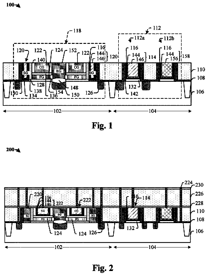
A mask programmable read-only memory (PROM) cell is provided utilizing a vertical transistor processing flow.
US 9,947,679 B2 · Assignee: RENESAS ELECTRONICS CORPORATION · Inventors: Owada; Fukuo et al.
Sheet 1 of 61 from the published document. All sheets in the USPTO PDF
An improvement is achieved in the performance of a semiconductor device. Over a first insulating film formed over a main surface of a semiconductor substrate located in a memory formation region and having an internal charge storage portion and over a second insulating film formed over the main surface of the semiconductor substrate located in a main circuit formation region, a conductive film is formed. Then, in the memory formation region, the conductive film and the first insulating film are patterned to form a first gate electrode and a first gate insulating film while, in the main circuit formation region, the conductive film and the second insulating film are left. Then, in the main circuit formation region, the conductive film and the second insulating film are patterned to form a second gate electrode and a second gate insulating film.
The present invention relates to a manufacturing technique for a semiconductor device and to, e.g., a technique which is effective when applied to a manufacturing technique for a semiconductor device in which a nonvolatile memory is embedded as an add-on circuit which is added to a main circuit including a field effect transistor. In a semiconductor device formed with a main circuit including a MISFET (Metal Insulator Semiconductor Field Effect Transistor) as a field effect transistor, an additional circuit (add-on circuit) which is added to the main circuit may be formed separately from the main circuit which provides the main function of the semiconductor device. Examples of the additional circuit include an electronic fuse used for the trimming or relief of the main circuit and a memory which stores trimming information. In recent years, there has been a growing need for an MTP (Multi
1 of 61 drawing sheets so far from the published document, cropped to the drawing. Every sheet is in the USPTO PDF.
What the patent claimed, word for word. All of it is now free to use.
The disclosure of Japanese Patent Application No. 2014-193860 filed on Sep. 24, 2014 including the specification, drawings and abstract is incorporated herein by reference in its entirety.
The present invention relates to a manufacturing technique for a semiconductor device and to, e.g., a technique which is effective when applied to a manufacturing technique for a semiconductor device in which a nonvolatile memory is embedded as an add-on circuit which is added to a main circuit including a field effect transistor.
In a semiconductor device formed with a main circuit including a MISFET (Metal Insulator Semiconductor Field Effect Transistor) as a field effect transistor, an additional circuit (add-on circuit) which is added to the main circuit may be formed separately from the main circuit which provides the main function of the semiconductor device. Examples of the additional circuit include an electronic fuse used for the trimming or relief of the main circuit and a memory which stores trimming information.
In recent years, there has been a growing need for an MTP (Multi Time Programmable) electronic fuse which uses a rewritable nonvolatile memory and can be adjusted many times. At present, as a memory which stores trimming information, a nonvolatile memory (NV memory) having a floating gate structure, which is appropriate for being embedded together with the field effect transistor included in a main circuit, is used. However, this increases the size of a memory cell and therefore a change to a nonvolatile memory which allows a reduction in the size of a memory cell is under consideration. In view of such a situation, in recent years, it has been considered to use a nonvolatile memory having a MONOS (Metal Oxide Nitride Oxide Semiconductor) structure as an additional circuit.
Each of US Patent Application Publication No. 2007/0102754 (Patent Document 1) and Japanese Unexamined Patent Publication No. 2002-324860 (Patent Document 2) discloses a technique which forms a nonvolatile memory element in a cell array region and forms a MISFET in a peripheral circuit region.
US Patent Application Publication No. 2008/0296664 (Patent Document 3) discloses a technique which forms a nonvolatile charge-trapping memory element in a first region and forms a logic element in a second region. US Patent Application Publication No. 2008/0150002 (Patent Document 4) discloses a technique which forms a SONOS (Silicon Oxide Nitride Oxide Semiconductor) transistor and a MISFET. International Publication No. WO 2013/149669 (Patent Document 5) discloses a technique which produces a tunnel oxide layer for a semiconductor storage device. RELATED ART DOCUMENTS Patent Documents
[Patent Document 1]
US Patent Application Publication No. 2007/0102754
[Patent Document 2]
Japanese Unexamined Patent Publication No. 2002-324860
[Patent Document 3]
US Patent Application Publication No. 2008/0296664
[Patent Document 4]
US Patent Application Publication No. 2008/0150002
[Patent Document 5]
International Publication No.
In the manufacturing process of such a semiconductor device in which a nonvolatile memory is embedded as an add-on circuit, when a conductive film and an insulating film are patterned in a memory formation region, the conductive film and the insulating film in a main circuit formation region may be patterned.
However, when the thickness of the insulating film is larger in the memory formation region than in the main circuit formation region, before the insulating film is etched and completely removed from the memory formation region, the insulating film is etched and removed from the main circuit formation region to expose the main surface of a semiconductor substrate. In addition, during the period when the insulating film is etched before completely removed from the memory formation region, the exposed upper surface of the semiconductor substrate is etched. In such a case, the upper surface of the semiconductor substrate may be damaged in the main circuit formation region. This causes the deterioration of the transistor properties of the MISFET formed in the main circuit formation region or the like to result in the deterioration of the performance of the semiconductor device.
Other problems and novel features of the present invention will become apparent from a statement in the present specification and the accompanying drawings.
According to an embodiment, in a method of manufacturing a semiconductor device, a conductive film is formed over a first insulating film formed over a main surface of a semiconductor substrate located in a first region and having an internal charge storage portion and over a second insulating film formed over the main surface of the semiconductor substrate located in a second region. Then, in the first region, the conductive film and the first insulating film are patterned to form a first gate electrode and a first gate insulating film, while the conductive film and the second insulating film are left in the second region. Then, in the second region, the conductive film and the second insulating film are patterned to form a second gate electrode and a second gate insulating film.
According to the embodiment, the performance of the semiconductor device can be improved.
FIG. 1 is a view showing an example of a layout configuration of a semiconductor chip in Embodiment 1;
FIG. 2 is a view showing an example of a circuit block configuration of a nonvolatile memory;
FIG. 3 is a main-portion cross-sectional view of a semiconductor device in Embodiment 1;
FIG. 4 is an illustrative view showing a memory array structure of the nonvolatile memory and an example of operating conditions;
FIG. 5 is a process flow chart showing a part of the manufacturing process of the semiconductor device in Embodiment 1;
FIG. 6 is a process flow chart showing a part of the manufacturing process of the semiconductor device in Embodiment 1;
FIG. 7 is a main-portion cross-sectional view of the semiconductor device in Embodiment 1 during the manufacturing process thereof;
FIG. 8 is a main-portion cross-sectional view of the semiconductor device in Embodiment 1 during the manufacturing process thereof;
FIG. 9 is a main-portion cross-sectional view of the semiconductor device in Embodiment 1 during the manufacturing process thereof;
FIG. 10 is a main-portion cross-sectional view of the semiconductor device in Embodiment 1 during the manufacturing process thereof;
FIG. 11 is a main-portion cross-sectional view of the semiconductor device in Embodiment 1 during the manufacturing process thereof;
FIG. 12 is a main-portion cross-sectional view of the semiconductor device in Embodiment 1 during the manufacturing process thereof;
FIG. 13 is a main-portion cross-sectional view of the semiconductor device in Embodiment 1 during the manufacturing process thereof;
FIG. 14 is a main-portion cross-sectional view of the semiconductor device in Embodiment 1 during the manufacturing process thereof;
FIG. 15 is a main-portion cross-sectional view of the semiconductor device in Embodiment 1 during the manufacturing process thereof;
FIG. 16 is a main-portion cross-sectional view of the semiconductor device in Embodiment 1 during the manufacturing process thereof;
FIG. 17 is a main-portion cross-sectional view of the semiconductor device in Embodiment 1 during the manufacturing process thereof;
FIG. 18 is a main-portion cross-sectional view of the semiconductor device in Embodiment 1 during the manufacturing process thereof;
FIG. 19 is a main-portion cross-sectional view of the semiconductor device in Embodiment 1 during the manufacturing process thereof;
FIG. 20 is a main-portion cross-sectional view of the semiconductor device in Embodiment 1 during the manufacturing process thereof;
FIG. 21 is a main-portion cross-sectional view of the semiconductor device in Embodiment 1 during the manufacturing process thereof;
FIG. 22 is a main-portion cross-sectional view of the semiconductor device in Embodiment 1 during the manufacturing process thereof;
FIG. 23 is a main-portion cross-sectional view of the semiconductor device in Embodiment 1 during the manufacturing process thereof;
FIG. 24 is a main-portion cross-sectional view of the semiconductor device in Embodiment 1 during the manufacturing process thereof;
FIG. 25 is a main-portion cross-sectional view of the semiconductor device in Embodiment 1 during the manufacturing process thereof;
FIG. 26 is a main-portion cross-sectional view of the semiconductor device in Embodiment 1 during the manufacturing process thereof;
FIG. 27 is a main-portion cross-sectional view of the semiconductor device in Embodiment 1 during the manufacturing process thereof;
FIG. 28 is a main-portion cross-sectional view of the semiconductor device in Embodiment 1 during the manufacturing process thereof;
FIG. 29 is a main-portion cross-sectional view of the semiconductor device in Embodiment 1 during the manufacturing process thereof;
FIG. 30 is a main-portion cross-sectional view of the semiconductor device in Embodiment 1 during the manufacturing process thereof;
FIG. 31 is a main-portion cross-sectional view of the semiconductor device in Embodiment 1 during the manufacturing process thereof;
FIG. 32 is a main-portion cross-sectional view of the semiconductor device in Embodiment 1 during the manufacturing process thereof;
FIG. 33 is a main-portion cross-sectional view of the semiconductor device in Embodiment 1 during the manufacturing process thereof;
FIG. 34 is a main-portion cross-sectional view of the semiconductor device in Embodiment 1 during the manufacturing process thereof;
FIG. 35 is a main-portion cross-sectional view of the semiconductor device in Embodiment 1 during the manufacturing process thereof;
FIG. 36 is a main-portion cross-sectional view of the semiconductor device in Embodiment 11 during the manufacturing process thereof;
FIG. 37 is a main-portion cross-sectional view of the semiconductor device in Embodiment 1 during the manufacturing process thereof;
FIG. 38 is a main-portion cross-sectional view of the semiconductor device in Embodiment 1 during the manufacturing process thereof;
FIG. 39 is a main-portion cross-sectional view of the semiconductor device in Embodiment 1 during the manufacturing process thereof;
FIG. 40 is a main-portion cross-sectional view of a semiconductor device in a comparative example during the manufacturing process thereof;
FIG. 41 is a graph showing the relationships between the gate length of a gate electrode and threshold voltages in a write operation and an erase operation in a MONOS transistor;
FIG. 42 is a main-portion cross-sectional view of a semiconductor device in Embodiment 2;
FIG. 43 is a process flow chart showing a part of the manufacturing process of the semiconductor device in Embodiment 2;
FIG. 44 is a main-portion cross-sectional view of the semiconductor device in Embodiment 2 during the manufacturing process thereof;
FIG. 45 is a main-portion cross-sectional view of the semiconductor device in Embodiment 2 during the manufacturing process thereof;
FIG. 46 is a main-portion cross-sectional view of the semiconductor device in Embodiment 2 during the manufacturing process thereof;
FIG. 47 is a main-portion cross-sectional view of the semiconductor device in Embodiment 2 during the manufacturing process thereof;
FIG. 48 is a main-portion cross-sectional view of the semiconductor device in Embodiment 2 during the manufacturing process thereof;
FIG. 49 is a main-portion cross-sectional view of the semiconductor device in Embodiment 2 during the manufacturing process thereof;
FIG. 50 is a main-portion cross-sectional view of the semiconductor device in Embodiment 2 during the manufacturing process thereof;
FIG. 51 is a main-portion cross-sectional view of the semiconductor device in Embodiment 2 during the manufacturing process thereof;
FIG. 52 is a main-portion cross-sectional view of the semiconductor device in Embodiment 2 during the manufacturing process thereof;
FIG. 53 is a main-portion cross-sectional view of the semiconductor device in Embodiment 2 during the manufacturing process thereof;
FIG. 54 is a main-portion cross-sectional view of the semiconductor device in Embodiment 2 during the manufacturing process thereof;
FIG. 55 is a main-portion cross-sectional view of the semiconductor device in Embodiment 2 during the manufacturing process thereof;
FIG. 56 is a main-portion cross-sectional view of the semiconductor device in Embodiment 2 during the manufacturing process thereof;
FIG. 57 is a process flow chart showing a part of the manufacturing process of a semiconductor device in Embodiment 3;
FIG. 58 is a main-portion cross-sectional view of the semiconductor device in Embodiment 3 during the manufacturing process thereof;
FIG. 59 is a main-portion cross-sectional view of the semiconductor device in Embodiment 3 during the manufacturing process thereof;
FIG. 60 is a main-portion cross-sectional view of the semiconductor device in Embodiment 3 during the manufacturing process thereof; and
FIG. 61 is a main-portion cross-sectional view of the semiconductor device in Embodiment 3 during the manufacturing process thereof.
In the following embodiments, if necessary for the sake of convenience, the embodiments will be each described by being divided into a plurality of sections or embodiments. However, they are by no means irrelevant to each other unless particularly explicitly described otherwise, but are in relations such that one of the sections or embodiments is a modification, details, supplementary explanation, and so forth of part or the whole of the others.
Also, in the following embodiments, when the number and the like (including the number, numerical value, amount, range, and the like) of elements are referred to, they are not limited to specific numbers unless particularly explicitly described otherwise or unless they are obviously limited to specific numbers in principle. The number and the like of the elements may be not less than or not more than specific numbers.
Also, in the following embodiments, it goes without saying that the components thereof (including also elements, steps, and the like) are not necessarily indispensable unless particularly explicitly described otherwise or unless the components are considered to be obviously indispensable in principle.
Likewise, if the shapes, positional relationships, and the like of the components and the like are referred to in the following embodiments, the shapes and the like are assumed to include those substantially proximate or similar thereto and the like unless particularly explicitly described otherwise or unless it can be considered that they obviously do not in principle. The same shall apply in regard to the foregoing numerical value and range.
Also, throughout all the drawings for illustrating the embodiments, the same members are designated by the same reference numerals, and a repeated description thereof is omitted. Note that, for improved clarity of illustration, even a plan view may be hatched. Embodiment 1
A technical idea in Embodiment 1 relates to a semiconductor device including, in the same semiconductor chip, a main circuit which provides the main function of a semiconductor chip and an additional circuit which is added to the main circuit and referred to as an add-on circuit. In the semiconductor device, the add-on circuit is formed of a MONOS rewritable nonvolatile memory.
For example, a SOC (System On Chip) includes a main circuit as shown below. That is, examples of the main circuit include a memory circuit such as a DRAM (Dynamic Random Access Memory) or an SRAM (Static Random Access Memory), a logic circuit such as a CPU (Central Processing Unit) or an MPU (Micro Processing Unit), and a mixed-signal circuit including a memory circuit and a logic circuit.
On the other hand, examples of the add-on circuit include a storage circuit which stores relatively low capacity information associated with the main circuit and an electronic fuse used to relieve a circuit. Examples of the relatively low capacity information include the location address information of elements used upon trimming in the semiconductor chip, the location address information of memory cells used in relieving the memory circuit, and the manufacturing number of the semiconductor device. When the semiconductor chip is an LCD (Liquid Crystal Display) driver, as the relatively low capacity information, trimming tap information for an adjustment voltage used in adjusting an LCD image can be listed.
<Example of Layout Configuration of Semiconductor Chip>
In Embodiment 1 shown below, a semiconductor chip formed with a system which provides a main function will be described as an example. The semiconductor chip in Embodiment 1 includes a lower-breakdown-voltage MISFET which is driven with a relatively low voltage, a higher-breakdown-voltage MISFET which is driven with a relatively high voltage to be capable of high-voltage driving, and a rewritable nonvolatile memory cell.
In a MISFET, a breakdown voltage refers to a pn-junction breakdown voltage which appears at the boundary between each of source/drain regions and a semiconductor substrate (well) which are included in the MISFET or the dielectric breakdown voltage of a gate insulating film. At this time, in Embodiment 1, a higher-breakdown-voltage MISFET having a relatively high breakdown voltage and a lower-breakdown-voltage MISFET having a relatively low breakdown voltage are formed in the semiconductor substrate.
FIG. 1 is a view showing an example of a layout configuration of a semiconductor chip in Embodiment 1. In FIG. 1 , a semiconductor chip CHP 1 includes a CPU 1 , a ROM (Read Only Memory) 2 , a RAM 3 , an analog circuit 4 , a nonvolatile memory 5 , and an I/O (Input/Output) circuit 6 .
The CPU 1 is referred to also as a central processing unit and corresponds to the heart of a computer or the like. The CPU 1 reads an instruction from a storage device, decodes the instruction, and performs various arithmetic and control operations on the basis of the decoded instruction and is required to perform high-speed processing. Accordingly, among the elements formed in the semiconductor chip CHP 1 , the MISFETs included in the CPU 1 need relatively large current driving forces. That is, the CPU 1 is formed of lower-breakdown-voltage MISFETs.
The ROM 2 is a memory in which stored information is fixed and cannot be changed and which is referred to as a read only memory. A configuration of the ROM 2 is subdivided into a NAND type in which MISFETs are coupled in series and a NOR type in which MISFETs are coupled in parallel. In most cases, the NAND type is used for an integration-density-oriented purpose, while the NOR type is used for an operation-speed-oriented purpose. The ROM 2 is also required to perform a high-speed operation so that the MISFETs included in the ROM 2 need relatively large current driving forces. That is, the ROM 2 is formed of lower-breakdown-voltage MISFETs.
The RAM 3 is a memory from which information stored therein can be read randomly, i.e., as necessary or information to be stored therein can newly be written. The RAM 3 is referred to also as a randomly writable/readable memory. The RAM 3 as an IC memory is subdivided into two types which are a DRAM (Dynamic RAM) using a dynamic circuit and an SRAM (Static RAM) using a static circuit. The DRAM is a randomly writable/readable memory which needs a memory retention operation, while the SRAM is a randomly writable/readable memory which does not need a memory retention operation. The RAM 3 is also required to perform a high-speed operation so that the MISFETs included in the RAM 3 need relatively large current driving forces. That is, the RAM 3 is formed of lower-breakdown-voltage MISFETs.
The analog circuit 4 handles voltage/current signals which continuously change with time, i.e., analog signals and includes, e.g., an amplification circuit, a conversion circuit, a modulation circuit, an oscillation circuit, a power supply circuit, and the like. For the analog circuit 4 , among the elements formed in the semiconductor chip CHP 1 , higher-breakdown-voltage MISFETs having relatively high breakdown voltages are used.
The nonvolatile memory 5 is a type of a nonvolatile memory which is electrically rewritable in each of a write operation and an erase operation and is referred to also as an electrically erasable programmable read only memory. In Embodiment 1, the nonvolatile memory 5 is formed of MONOS transistors. For a write operation and an erase operation to a MONOS transistor, e.g., a Fowler-Nordheim (FN) tunneling phenomenon is used. Note that it is also possible to allow a write operation or an erase operation to be performed using hot electrons or hot holes.
During a write operation to the nonvolatile memory 5 or the like, a large potential difference (of about 12 V) is applied to the MONOS transistors. Accordingly, as the MONOS transistors, relatively-high-breakdown-voltage transistors are needed.
The I/O circuit 6 is an input/output circuit for outputting data from within the semiconductor chip CHP 1 to an external device coupled to the semiconductor chip CHP 1 and inputting data from the external device coupled to the semiconductor chip CHP 1 into the semiconductor chip CHP 1 . The I/O circuit 6 is formed of relatively-high-breakdown-voltage MISFETs.
Here, the CPU 1 , the ROM 2 , the RAM 3 , and the analog circuit 4 form a main circuit, while the nonvolatile memory 5 forms an add-on circuit. That is, in the semiconductor chip CHP 1 in Embodiment 1, the main circuit which provides the main function and the add-on circuit which is added to the main circuit are formed. In Embodiment 1, by applying MONOS transistors to the add-on circuit, advantages shown below can be obtained.
For example, the add-on circuit includes an electronic fuse, and the electronic fuse is formed of MONOS transistors as a rewritable nonvolatile memory. This offers the advantage of allowing an MTP (Multi Time Programmable) electronic fuse to be implemented. The MTP electronic fuse can be adjusted many times in a wafer state or in a package state.
Also, for example, as a memory which stores trimming information, a nonvolatile memory (NV memory) having a floating gate structure which is appropriate for being embedded together with the field effect transistor included in the main circuit is used. However, the use of the nonvolatile memory having the floating gate structure increases the size of a memory cell. In view of this, MONOS transistors are used appropriately instead of the nonvolatile memory (NV memory) having the floating gate structure to offer the advantage of allowing a reduction in the size of the memory cell. In addition, since the MONOS transistors use an FN tunneling current for rewriting data, low-current data rewriting can be performed to achieve a reduction in power consumption.
The semiconductor device in Embodiment 1 includes the main circuit and the add-on circuit. In implementing the semiconductor device in which the MONOS transistors are used appropriately as the add-on circuit, the semiconductor device in Embodiment 1 is characterized by a manufacturing technique therefor. That is, the semiconductor device in Embodiment 1 is characterized by the manufacturing technique therefor which embeds the MONOS transistors as the components of the add-on circuit together with lower-breakdown-voltage MISFETs and higher-breakdown-voltage MISFETs as the components of the main circuit.
<Circuit Block Configuration of Nonvolatile Memory>
FIG. 2 is a view showing an example of a circuit block configuration of the nonvolatile memory. In FIG. 2 , the nonvolatile memory 5 includes a memory array 10 , a direct peripheral circuit portion 11 , and an indirect peripheral circuit portion 12 .
The memory array 10 corresponds to the storage portion of the nonvolatile memory 5 . The large number of memory cells are arranged vertically and laterally in a two-dimensional configuration (array configuration). Each of the memory cells is a circuit for storing 1-bit unit information and is formed of the MONOS transistor as the storage portion.
The direct peripheral circuit portion 11 is a circuit for driving the memory cell array 10 , i.e., a drive circuit and includes, e.g., a boosting circuit which generates, from a power supply voltage, a voltage several times higher than the power supply voltage, a boosting clock generation circuit, a voltage clamp circuit, a column decoder and a row address decoder each for selecting a row and a column, a column latch circuit, a WELL control circuit, and the like. The MISFETs included in the direct peripheral circuit portion 11 are formed of higher-breakdown-voltage MISFETs which need relatively high breakdown voltages among the elements formed in the semiconductor chip CHP 1 .
The indirect peripheral circuit portion 12 is a circuit which controls rewriting to the memory array and includes a setting circuit, a normal-rewrite clock generator, a high-speed-rewrite clock generator, a rewrite timing controller, and the like. The MISFETs included in the indirect peripheral circuit portion 12 are formed of the lower-breakdown-voltage MISFETs which are driven with relatively low voltages and capable of high-speed operations among the elements formed in the semiconductor chip CHP 1 .
<Structure of Semiconductor Device>
Next, a structure of the semiconductor chip CHP 1 as the semiconductor device in Embodiment 1 will be described with reference to the drawings. FIG. 3 is a main-portion cross-sectional view of the semiconductor device in Embodiment 1.
As shown in FIG. 3 , the semiconductor chip CHP 1 as the semiconductor device in Embodiment 1 includes a memory formation region MR and a main circuit formation region AR. The main circuit formation region AR includes a lower-breakdown-voltage MISFET formation region LR and a higher-breakdown-voltage MISFET formation region HR.
In the memory formation region MR, the memory cells of the nonvolatile memory 5 shown in FIG. 1 are formed. The memory cells are formed of MONOS transistors MC.
In the lower-breakdown-voltage MISFET formation region LR, a lower-breakdown-voltage MISFET QL which needs a large current driving force to be capable of a high-speed operation is formed. As examples of a region where the lower-breakdown-voltage MISFET QL is formed, regions where the CPU 1 , the ROM 2 , and the RAM 3 are formed can be considered. The lower-breakdown-voltage MISFET QL operates with a power supply voltage of, e.g., about 1.5 V.
On the other hand, in the higher-breakdown-voltage MISFET formation region HR, a higher-breakdown-voltage MISFET QH is formed. As examples of a region where the higher-breakdown-voltage MISFET QH is formed, a region where the analog circuit 4 is formed and a region where the I/O circuit 6 is formed can be considered. The higher-breakdown-voltage MISFET QH operates with a power supply voltage of, e.g., about 5 V.
As shown in FIG. 3 , the semiconductor chip CHP 1 includes a semiconductor substrate SB. In an upper surface PS as the main surface of the semiconductor substrate SB, isolation regions STI which isolate elements from each other are formed. The active regions isolated by the isolation regions STI are the memory formation region MR, the lower-breakdown-voltage MISFET formation region LR, and the higher-breakdown-voltage MISFET formation region HR. That is, the memory formation region MR, the lower-breakdown-voltage MISFET formation region LR, and the higher-breakdown-voltage MISFET formation region HR are local regions of the upper-surface PS of the semiconductor substrate SB. In the memory formation region MR, on the upper surface PS side of the semiconductor substrate SB, a p-type well PWM is formed. Likewise, in the lower-breakdown-voltage MISFET formation region LR, on the upper surface PS side of the semiconductor substrate SB, a p-type well PWL is formed while, in the higher-breakdown-voltage MISFET formation region HR, on the upper surface PS side of the semiconductor substrate SB, a P-type well PWH is formed. Note that “p-type” means a conductivity type using a hole as a main charge carrier.
In Embodiment 1, n-channel MISFETs are described as an example of the MISFETs formed in the lower-breakdown-voltage MISFET formation region LR and the higher-breakdown-voltage MISFET formation region HR. However, p-channel MISFETs may also be formed in each of the regions.
Next, a description will be given of the MONOS transistor MC shown in FIG. 3 . The MONOS transistor MC includes the p-type well PWM, a gate insulating film GIM, a gate electrode CG, sidewall spacers SW, n.sup.−-type semiconductor regions LDM, and n.sup.+-type semiconductor regions NDM. That is, the nonvolatile memory is formed of the gate electrode CG and the gate insulating film GIM. The gate insulating film GIM includes an insulating film IF 1 made of, e.g., silicon dioxide, a charge storage film EC as an insulating film made of, e.g., silicon nitride, and an insulating film IF 2 made of, e.g., silicon dioxide and is referred to also as an ONO (Oxide-Nitride-Oxide) film. Note that each of “n.sup.−-type” and “n.sup.+-type” means an conductivity type opposite to the p-type conductivity type and using an electron as a main charge carrier.
Over the p-type well PWM formed on the upper surface PS side of the semiconductor substrate SB, the insulating film IF 1 is formed and, over the insulating film IF 1 , the charge storage film EC is formed. Over the charge storage film EC, the insulating film IF 2 is formed and, over the insulating film IF 2 , the gate electrode CG made of a conductive film is formed. The gate electrode CG is made of, e.g., a polysilicon film.
Over the both side surfaces of the gate electrode CG, the sidewall spacers SW as side-wall portions each made of, e.g., an insulating film are formed to form LDD (lightly Doped Drain) structures. In the upper-layer portions of the parts of the p-type well PWM which are located under the sidewall spacers SW, the n.sup.−-type semiconductor regions LDM are formed. In the upper-layer portions of the parts of the p-type well PWM which are located outside the n.sup.−-type semiconductor regions LDM in plan view, the n.sup.+-type semiconductor regions NDM are formed. The n.sup.+-type semiconductor regions NDM are in contact with the n.sup.−-type semiconductor regions LDM. An impurity concentration in each of the n.sup.+-type semiconductor regions NDM is higher than an impurity concentration in each of the n.sup.−-type semiconductor regions LDM. In the upper-layer portion of the part of the p-type well PWM which is located immediately under the insulating film IF 1 , a channel region is formed. Over the respective upper surfaces of the gate electrode CG and the n.sup.−-type semiconductor regions NDM, silicide films CS are formed to reduce resistances.
The insulating film IF 1 is made of, e.g., silicon dioxide. When electrons are injected from the semiconductor substrate SB into the charge storage film EC via the insulating film IF 1 or the electrons stored in the charge storage film EC are released into the semiconductor substrate SB to store or erase data, the insulating film IF 1 functions as a tunnel insulating film.
The charge storage film EC is an insulating film provided as a charge storage portion where charges contributing to data storage are stored and made of, e.g., silicon nitride. Accordingly, the gate insulating film GIM includes the charge storage film EC as the charge storage portion.
Conventionally, as the charge storage film EC, a polysilicon film has mainly been used. However, in the case of using a polysilicon film as the charge storage film EC, when there is a defect in any part of an oxide film surrounding the charge storage film EC, all the charges stored in the charge storage film EC, which is a conductor, may leak away as a result of abnormal leakage.
Accordingly, as described above, an insulating film made of silicon nitride has been used as the charge storage film EC. In this case, the charges contributing to data storage are stored at discrete trap levels (capture levels) present in the charge storage film EC. As a result, even when a defect occurs in a part of the oxide film surrounding the charge storage film EC, since the charges are stored at the discrete trap levels in the charge storage film EC, there is no situation where all the charges leak away from the charge storage film EC. This allows an improvement in the reliability of data retention.
For a reason as stated above, by using not only an insulating film made of silicon nitride, but also a film containing discrete trap levels as the charge storage film EC, it is possible to achieve an improvement in the reliability of data retention.
The insulating film IF 2 is made of, e.g., silicon dioxide. When data is stored or erased by injecting electrons from the gate electrode CG into the charge storage film EC via the insulating film IF 2 or releasing the electrons stored in the charge storage film EC into the gate electrode CG, the insulating film IF 2 functions as a tunnel insulating film.
The sidewall spacers SW are formed to provide each of the source region and the drain region as the semiconductor regions of the MONOS transistor MC with an LDD structure. That is, each of the source region and the drain region of the MONOS transistor MC is formed of the n.sup.−-type semiconductor region LDM and the n.sup.+-type semiconductor region NDM. At this time, by forming each of the source region under the gate electrode CG and the drain region under the gate electrode CG of the n.sup.−-type semiconductor region LDM, it is possible to suppress the concentration of an electric field under each of the end portions of the gate electrode CG.
Next, a description will be given of a lower-breakdown-voltage MISFET QL. The lower-breakdown-voltage MISFET QL includes the p-type well PWL, a gate insulating film GIL, a gate electrode GEL, the sidewall spacers SW, n.sup.−-type semiconductor regions LDL, and n.sup.+-type semiconductor regions NDL.
Over the p-type well PWL formed on the upper surface PS side as the main surface of the semiconductor substrate SB, the gate insulating film GIL is formed and, over the gate insulating film GIL, the gate electrode GEL is formed. The gate insulating film GIL is made of, e.g., silicon dioxide. The gate electrode GEL is made of, e.g., a polysilicon film.
Over the both side surfaces of the gate electrode GEL, the sidewall spacers SW as side-wall portions each made of, e.g., an insulating film are formed. In the upper-layer portions of the parts of the p-type well PWL which are located under the sidewall spacers SW, the n.sup.−-type semiconductor regions LDL are formed. In the upper-layer portions of the parts of the p-type well PWL which are located outside the n.sup.−-type semiconductor regions LDL in plan view, the n.sup.+-type semiconductor regions NDL are formed. The n.sup.+-type semiconductor regions NDL are in contact with the n.sup.−-type semiconductor regions LDL. An impurity concentration in each of the n.sup.+-type semiconductor regions NDL is higher than an impurity concentration in each of the n.sup.−-type semiconductor regions LDL. In the upper-layer portion of the part of the p-type well PWL which is located immediately under the gate insulating film GIL, a channel region is formed. Over the respective upper surfaces of the gate electrode GEL and the n.sup.+-type semiconductor regions NDL, the silicide layers CS are formed to reduce resistances.
Subsequently, a description will be given of the higher-breakdown-voltage MISFET QH. The higher-breakdown-voltage MISFET QH includes a p-type well PWH, a gate insulating film GIH, a gate electrode GEH, the sidewall spacers SW, n.sup.−-type semiconductor regions LDH, and n.sup.+-type semiconductor regions NDH.
Over the p-type well PWH formed on the upper surface PS side as the main surface of the semiconductor substrate SB, the gate insulating film GIH is formed and, over the gate insulating film GIH, the gate electrode GEH is formed. The gate insulating film GIH is made of, e.g., silicon dioxide. The gate electrode GEH is made of, e.g., a polysilicon film.
Over the both side surfaces of the gate electrode GEH, the sidewall spacers SW as side-wall portions each made of, e.g., an insulating film are formed. In the upper-layer portions of the parts of the p-type well PWH which are located under the sidewall spacers SW, the n.sup.−-type semiconductor regions LDH are formed. In the upper-layer portions of the parts of the p-type well PWH which are located outside the n.sup.−-type semiconductor regions LDH in plan view, the n.sup.+-type semiconductor regions NDH are formed. The n.sup.+-type semiconductor regions NDH are in contact with the n.sup.−-type semiconductor regions LDH. An impurity concentration in each of the n.sup.+-type semiconductor regions NDH is higher than an impurity concentration in each of the n.sup.−-type semiconductor regions LDH. In the upper-layer portion of the part of the p-type well PWH which is located immediately under the gate insulating film GIH, a channel region is formed. Over the respective upper surfaces of the gate electrode GEH and the n.sup.+-type semiconductor regions NDH, the silicide layers CS are formed to reduce resistances.
To the higher-breakdown-voltage MISFET QH, a voltage higher than that applied to the lower-breakdown-voltage MISFET QL is applied. Accordingly, the thickness of the gate insulating film GIH of the higher-breakdown-voltage MISFET QH is larger than the thickness of the gate insulating film GIL of the lower-breakdown-voltage MISFET QL. This can improve the dielectric strength of the gate insulating film GI of the higher-breakdown-voltage MISFET QH. That is, it is possible to increase the breakdown voltage of the higher-breakdown-voltage MISFET QH.
Note that, in FIG. 3 , the difference between the respective gate lengths of the gate electrodes GEH and GEL is not shown, but the gate length of the gate electrode GEH may also be longer than the gate length of the gate electrode GEL. By reducing the gate length of the gate electrode GEL in the lower-breakdown-voltage MISFET QL, it is possible to reduce the resistance between the source region and the drain region and improve a current driving force. On the other hand, by increasing the gate length of the gate electrode GEH in the higher-breakdown-voltage MISFET QH, even when a relatively high potential is applied, it is possible to prevent a punch-through from occurring between the source region and the drain region.
Note that the thickness of the gate insulating film GIM of the MONOS transistor MC is larger than the thickness of the gate insulating film GIL of the lower-breakdown-voltage MISFET QL. In such a case, the effect of forming the gate insulating film GIL in a step subsequent to the step of forming the gate insulating film GIM becomes prominent.
Over the semiconductor substrate SB, an insulating film SNF has been formed so as to cover the MONOS transistor MC, the lower-breakdown-voltage MISFET QL, and the higher-breakdown-voltage MISFET QH. For example, the insulating film SNF is made of, e.g., silicon nitride or the like.
Over the insulating film SNF, an interlayer insulating film IL 1 is formed. The interlayer insulating film IL is made of an insulating film made of silicon dioxide, a laminated film including an insulating film made of silicon nitride and an insulating film made of silicon dioxide, or the like. The upper surface of the interlayer insulating film IL 1 has been planarized.
The description continues in the full USPTO document.
About 6,305 words. The USPTO PDF has it with every drawing.
Fees are due 3.5, 7.5 and 11.5 years after grant. This patent expired on April 17, 2026, so the fee marked "not paid" was the one that went unpaid.
METHOD OF MANUFACTURING A SEMICONDUCTOR DEVICE
Filed Sep 2015 · published Mar 2016Method of manufacturing semiconductor device with separately formed insulating films in main circuit and memory regions
Filed Sep 2015 · granted Apr 2018Earlier publications, parents and continuations. None of them can still be enforced, or this patent would not be listed.
Prior art cited by the examiner or applicant. Useful when you check your own idea for novelty.
Everything on this page comes from the documents linked above.