Background
Field of the Disclosure
The present disclosure relates to an image pickup apparatus having a global electronic shutter, an image pickup system, and a control method for the image pickup apparatus.
Description of the Related Art
In recent years, a global electronic shutter has been proposed for a complementary metal-oxide semiconductor (CMOS) image sensor. For example, image pickup apparatuses described in Japanese Patent Laid-Open No. 2004-111590 and Japanese Patent Laid-Open No. 2011-188410 use the global electronic shutter to avoid distortion of a fast-moving object image.
In the image pickup apparatus described in Japanese Patent Laid-Open No. 2004-111590, all charges generated by photoelectric conversion are accumulated in a charge generation unit, and thereafter, the charges are transferred at the same time from a photoelectric conversion unit to a charge accumulation unit in all pixels. As a result, the global electronic shutter is realized.
In the image pickup apparatus described in Japanese Patent Laid-Open No. 2011-188410, to correct a pseudo signal that may be generated in a first charge accumulation unit, a configuration is adopted in which a signal equivalent to the pseudo signal can be obtained from a second charge accumulation unit. During a period in which the first charge accumulation unit holds the charges, the signal equivalent to the pseudo signal is read out by driving the second charge accumulation unit. Japanese Patent Laid-Open No. 2011-188410 describes that it is possible to correct the signal held in the first charge accumulation unit by using the thus obtained signal indicating the pseudo signal component.
However, according to the technique described in Japanese Patent Laid-Open No. 2011-188410, an accuracy of the signal for the correction is not sufficient in some cases.
Summary
The present disclosure has been made in view of the above-described circumstances, and the present disclosure provides an image pickup apparatus that may obtain the signal for the correction at a still higher accuracy.
An image pickup apparatus according to an aspect of the present disclosure includes a plurality of pixels, each of the plurality of pixels including a photoelectric conversion unit configured to perform accumulation of charges generated by incident light, a holding unit configured to hold the charges, an amplification unit configured to output a signal based on the charges, a first transfer switch configured to transfer the charges from the photoelectric conversion unit to the holding unit, and a second transfer switch configured to transfer the charges from the holding unit to the amplification unit, in which the photoelectric conversion unit in each of the plurality of pixels starts the accumulation of the charges at a first time, the first transfer switch in each of the plurality of pixels is controlled to be turned on after the first time and to be thereafter turned off at a second time to transfer the charges accumulated in the photoelectric conversion unit to the holding unit, the second transfer switch in at least one pixel among the plurality of pixels is controlled to be turned on at a third time after the second time to transfer the charges held in the holding unit to the amplification unit, the second transfer switch in the at least one pixel is controlled to be turned on at a fourth time after the third time to transfer the charges held in the holding unit to the amplification unit, and the first transfer switch in the at least one pixel is maintained to be in an off state during a period from the third time to the fourth time.
Further features of the present disclosure will become apparent from the following description of exemplary embodiments with reference to the attached drawings.
Brief description of the drawings
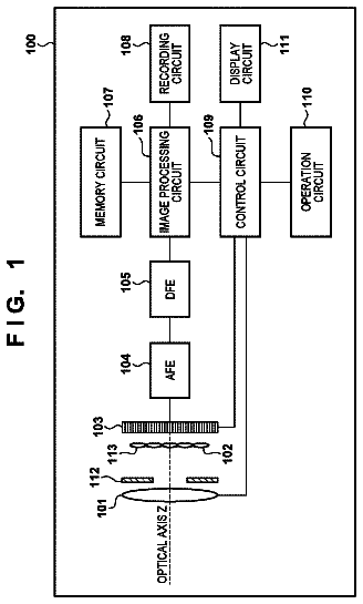
FIG. 1 is a block diagram illustrating a schematic configuration of an image pickup apparatus according to one or more aspects of the present disclosure.
FIG. 2 illustrates an equivalent circuit of a pixel in the image pickup apparatus according to one or more aspects of the present disclosure.
FIG. 3 schematically illustrates a section structure of the pixel in the image pickup apparatus according to one or more aspects of the present disclosure.
FIG. 4 schematically illustrates an operation of the image pickup apparatus according to one or more aspects of the present disclosure.
FIG. 5 is a timing chart for control signals of the image pickup apparatus according to one or more aspects of the present disclosure.
FIG. 6 is a timing chart for the pixel in the image pickup apparatus according to one or more aspects of the present disclosure.
FIG. 7 schematically illustrates the operation of the image pickup apparatus according to one or more aspects of the present disclosure.
FIG. 8 is a timing chart for the control signals of the image pickup apparatus according to one or more aspects of the present disclosure.
FIG. 9 schematically illustrates the operation of the image pickup apparatus according to one or more aspects of the present disclosure.
FIG. 10 is a timing chart for the control signals of the image pickup apparatus according to one or more aspects of the present disclosure.
FIG. 11 schematically illustrates the operation of the image pickup apparatus according to one or more aspects of the present disclosure.
FIG. 12 is a timing chart for the control signals of the image pickup apparatus according to one or more aspects of the present disclosure.
FIG. 13 schematically illustrates the operation of the image pickup apparatus according to one or more aspects of the present disclosure.
FIG. 14 is a timing chart for the control signals of the image pickup apparatus according to one or more aspects of the present disclosure.
FIG. 15 is a block diagram of an image pickup system according to one or more aspects of the present disclosure.
Description of the embodiments
An image pickup apparatus according to some exemplary embodiments of the present disclosure is provided with a plurality of pixels, and each of the pixels includes a photoelectric conversion unit, a holding unit configured to hold signal charges, and an amplification unit configured to output a signal based on the charges. The pixel is further provided with a first transfer transistor configured to transfer real signal charges from the photoelectric conversion unit to the holding unit, a second transfer transistor configured to transfer the charges from the holding unit to the amplification unit, and an overflow transistor configured to discharge the charges of the photoelectric conversion unit. According to the above-described configuration, it is possible to perform an image pickup operation that is so-called a global electronic shutter in which periods for photoelectric conversion are matched with one another among the plurality of pixels. An electronic shutter refers to an image pickup operation of electrically controlling accumulation of the real signal charges generated by incident light.
During a first reading period in each of frames, a plurality of second transfer transistors are sequentially turned on, so that the real signal charges in the previous frame are sequentially transferred from the holding unit to the amplification unit (first read). It should be noted that a signal obtained by this first read includes second pseudo signal charges generated in the holding unit in the previous frame in addition to the real signal charges in the previous frame. This accumulation of the second pseudo signal charges will be described below. After the transfer of the real signal charges is ended, the accumulation of first pseudo signal charges is started in the holding unit.
During a second reading period after the end of the first reading period, the plurality of second transfer transistors are sequentially turned on, so that the accumulation of the first pseudo signal charges is ended, and the first pseudo signal charges are sequentially transferred from the holding unit to the amplification unit (second read). The holding unit that has ended the transfer of the first pseudo signal charges starts the accumulation of the second pseudo signal charges and also is put into a state to stand by for the transfer of the real signal charges from the first transfer transistor. Thereafter, the first read is similarly performed in the above-described manner, and the real signal charges and the second pseudo signal charges are read out again.
In this manner, the first read for reading out the real signal charges and the second pseudo signal charges and the second read for reading out the first pseudo signal charges are performed in each of the frames. Herein, the number of signals output during the first and second reading periods may be changed depending on a format of an image output by the image pickup apparatus. For example, in a case where the image pickup apparatus performs imaging of a moving image, the number of signals corresponding to the number of horizontal lines used in one frame may be output. It should be noted that signals do not necessarily need to be output from all the pixels included in the image pickup apparatus. For example, a configuration may be adopted in which signals are output from only part of the pixel in the image pickup apparatus. In this case, time used to perform the read operation may be shortened.
According to some exemplary embodiments of the present disclosure, the accumulation of the first pseudo signal charges and the accumulation of the second pseudo signal charges are performed in the same holding unit. For this reason, as compared with a case where the accumulation of the first pseudo signal charges and the accumulation of the second pseudo signal charges are performed in different elements as described in Japanese Patent Laid-Open No. 2011-188410, it is possible to obtain the signal for correcting the pseudo signal at a still higher accuracy. Therefore, when the correction is performed by using this signal, the image quality degradation caused by pseudo signal charges can be further alleviated. Thus, the image pickup apparatus according to some exemplary embodiments of the present disclosure can obtain the high quality image while the global electronic shutter operation is realized.
According to a first exemplary embodiment, the first and second reading periods may be the same length, but according to some of the other exemplary embodiments, the second reading period for outputting the first pseudo signal charges may be set to be shorter than the first reading period. The charge amount of the pseudo signal charges is lower in many cases with respect to the real signal charges. This is because the time used to perform the read operation may be shortened in the above-described case. Thus, the time used for the one frame can be shortened, so that it is possible to increase a frame rate. In addition, in a case where the frame rate is set to be constant, it is possible to reduce power consumption and reduce noise.
The image pickup apparatus according to one exemplary embodiment of the present disclosure continuously performs the first read for reading out the real signal charges and the second pseudo signal charges and the second read for reading out the first pseudo signal charges in the same row. Since it is possible to continuously obtain the real signal charges and the pseudo signal charges for the one row, it is not necessary to hold the signal for each frame in another storage unit such as a frame memory, and it is possible to simplify a configuration of an image pickup system.
Hereinafter, exemplary embodiments of the present disclosure will be described with reference to the drawings. The present disclosure is not limited to exemplary embodiments described below. For example, part of the configuration according to any one of the exemplary embodiments described below may be added to and combined with another exemplary embodiment. Alternatively, part of the configuration according to any one of the exemplary embodiments may be replaced with part of a configuration according to another exemplary embodiment. First Exemplary Embodiment
FIG. 1 is a block diagram illustrating a schematic configuration of an image pickup apparatus according to the present exemplary embodiment. The image pickup apparatus is provided with a pixel unit 100 , a vertical scanning circuit 101 , a column amplification circuit 102 , a horizontal scanning circuit 103 , an output circuit 104 , and a control circuit 105 . The pixel unit 100 is provided with a plurality of pixels 10 arranged so as to form a plurality of rows and a plurality of columns. The vertical scanning circuit 101 supplies a control signal for controlling a plurality of transistors included in the pixel 10 to be turned on (conductive state) or off (non-conductive state). A column signal line 5 is provided in each column of the pixel 10 , and a signal from the pixel 10 is read out to the column signal line 5 for each column. The column amplification circuit 102 amplifies a pixel signal output to the column signal line 5 , and processing such as correlated double sampling processing based on a signal at the time of resetting and a signal at the time of photoelectric conversion in the pixel 10 is performed. The horizontal scanning circuit 103 supplies a control signal for controlling a switch connected to an amplifier of the column amplification circuit 102 to be turned on or off. The output circuit 104 is constituted by a buffer amplifier, a differential amplifier, or the like and outputs the pixel signal from the column amplification circuit 102 to a signal processing unit outside the image pickup apparatus. It should be noted that the column amplification circuit 102 inside the image pickup apparatus may include a function of a signal processing circuit configured to perform signal processing such as correction of a pseudo signal component. In addition, an analog-to-digital (AD) conversion unit may be provided to the image pickup apparatus to output a digital pixel signal.
FIG. 2 illustrates an equivalent circuit of the pixel 10 in the image pickup apparatus according to the present exemplary embodiment. FIG. 2 illustrates the nine pixels 10 in three rows×three columns among the plurality of pixels 10 that are two-dimensionally arranged in a row direction and a column direction. However, this is an exemplification illustrating part of the plurality of pixels 10 , and the image pickup apparatus may include further more pixels. Each of the pixels 10 is provided with a photoelectric conversion unit 1 , a holding unit 2 , a floating diffusion region 3 , a transfer transistor M 1 , a second transfer transistor M 2 , an amplification transistor M 3 , a selection transistor M 4 , a reset transistor M 5 , and an overflow transistor M 6 .
The photoelectric conversion unit 1 performs photoelectric conversion of incident light and also accumulates the real signal charges generated by the photoelectric conversion. When the first transfer transistor M 1 (first transfer switch) is turned on, the first transfer transistor M 1 transfers the real signal charges of the photoelectric conversion unit 1 to the holding unit 2 . The holding unit 2 holds the real signal charges transferred from the photoelectric conversion unit 1 . When the second transfer transistor M 2 (second transfer switch) is turned on, the second transfer transistor M 2 transfers the charges of the holding unit 2 to the floating diffusion region 3 of the amplification transistor M 3 . A drain of the amplification transistor M 3 is connected to a power source voltage line 4 , and a source of the amplification transistor M 3 is connected to the column signal line 5 via the selection transistor M 4 . A constant current source 16 is connected to the column signal line 5 . An output signal Vout is output to the column amplification circuit 102 via the column signal line 5 in each column. When the reset transistor M 5 (reset switch) is turned on, the reset transistor M 5 resets a voltage of the floating diffusion region 3 . A source of the overflow transistor M 6 is connected to the photoelectric conversion unit 1 , and a drain of the overflow transistor M 6 is connected to a power source node. A control signal OFG is applied to a gate of the overflow transistor M 6 . When the overflow transistor M 6 (discharge switch) is turned on, the overflow transistor M 6 can discharge the charges of the photoelectric conversion unit 1 to an overflow drain such as the power source node. When the overflow transistor M 6 is controlled from an on state to an off state, the accumulation of the charges by the photoelectric conversion unit 1 is started. As a result, it is possible to freely set an exposure time.
In the following descriptions, the floating diffusion region 3 , the amplification transistor M 3 , the selection transistor M 4 , and the reset transistor M 5 may be collectively referred to as an output unit. In addition, the floating diffusion region 3 and the amplification transistor M 3 function as an amplification unit configured to output a voltage based on the transferred charges. Signal charges obtained from the photoelectric conversion in the photoelectric conversion unit 1 by the incident light are referred to as real signal charges. In contrast to this, signal charges generated by occurrence of photoelectric conversion in a unit other than the photoelectric conversion unit 1 such as, for example, the holding unit 2 , charges generated by leakage of the charges, and the like are referred to as pseudo signal charges, which will be described while being distinguished from the above-described real signal charges.
It should be noted that the provision of the overflow transistor M 6 is optional, and the overflow transistor M 6 may be omitted. In a case where the overflow transistor M 6 is omitted, when the first transfer transistor M 1 is controlled from the on state to the off state, the accumulation of the charges by the photoelectric conversion unit 1 is started, and it is possible to set the exposure time. According to this configuration, although a restriction is imposed on an operation method for each of the transistors for setting the exposure time, the number of elements is decreased, so that a degree of freedom for the layout is improved.
In addition, as another modified example, a configuration called vertical overflow may be adopted in which a charge discharge destination from the photoelectric conversion unit is set as a semiconductor substrate. According to this configuration, since the number of elements arranged on a substrate surface is decreased, the degree of freedom for the layout is improved.
A common control signal is supplied to the pixels 10 in the same row from the vertical scanning circuit 101 . That is, a control signal TX 1 ( m ) is supplied to the gate of the first transfer transistor M 1 included in each of the plurality of pixels 10 arranged in the m-th row. Similarly, a control signal TX 2 ( m ) is supplied to a gate of the second transfer transistor M 2 in the m-th row. A control signal SEL(m) is supplied to a gate of the selection transistor M 4 in the m-th row. The control signal RES(m) is supplied to a gate of the reset transistor M 5 in the m-th row. The control signal OFG(m) is supplied to the gate of the overflow transistor M 6 in the m-th row. It should be noted that a subscript m for each of the control signals indicates a row number, and the subscript is assigned in a case where it is necessary to explicate a control signal related to a particular row in the following descriptions.
These transistors are turned on when the respective control signals are at a high level and are turned off when the respective control signals are at a low level. When the control signals in the respective rows are controlled to be turned on or off at the same time, it is possible to control the exposure times in the plurality of pixels 10 to be in the same period of time. According to the above-described configuration, while the holding unit 2 holds the charges, the photoelectric conversion unit 1 can accumulate newly generated charges, and it is possible to perform the global electronic shutter operation in which the periods of the photoelectric conversions in the plurality of pixels are matched with one another.
It should be noted that each of the plurality of pixels 10 includes the amplification unit in the circuit illustrated in FIG. 2 , but the plurality of pixels 10 may share a single amplification unit. In addition, the pixel unit 100 may also include a pixel that does not output a signal for constituting an image, such as a light shielded pixel in which the photoelectric conversion unit 1 is light-shielded or a dummy pixel that does not include the photoelectric conversion unit 1 , other than effective pixel such as the pixel 10 illustrated in FIG. 2 .
FIG. 3 schematically illustrates a section structure of the pixel 10 in the image pickup apparatus according to the present exemplary embodiment.
The photoelectric conversion unit 1 is arranged in a well region 14 of a P-type and includes a semiconductor region 11 of an N-type and a semiconductor region 12 of the P-type. The semiconductor region 11 and the semiconductor region 12 form a PN junction and constitute a buried type photodiode structure. Photoelectric conversion of the incident light is performed in the PN junction, and charges generated by the photoelectric conversion are accumulated in the semiconductor region 11 of the N-type. At this time, since a PN junction interface is buried in the substrate by the semiconductor region 12 of the P-type, noise is suppressed.
A semiconductor region 13 of the N-type is arranged on a lower surface of the photoelectric conversion unit 1 . An impurity concentration of the semiconductor region 13 is lower than an impurity concentration of the semiconductor region 11 of the same N-type. As a result, charges generated at a deep position in the semiconductor substrate are captured in the semiconductor region 13 , and the noise is suppressed. The semiconductor region 13 may be of the P-type. Furthermore, a semiconductor region 15 of the P-type functioning as a potential barrier with respect to the charges is arranged on a lower surface of the semiconductor region 13 .
The holding unit 2 includes a semiconductor region 21 of the N-type arranged in the well region 14 of the P-type. The charges transferred from the photoelectric conversion unit 1 are held by the semiconductor region 21 . According to the present exemplary embodiment, an impurity concentration of the semiconductor region 21 is higher than the impurity concentration of the semiconductor region 11 of same the N-type.
A gate electrode 40 is arranged on an upper side of the well region 14 between the semiconductor region 12 and the semiconductor region 21 via a gate insulating film and constitutes the gate of the first transfer transistor M 1 . In a case where a voltage of the gate electrode 40 is positive, the first transfer transistor M 1 is put into the on state, and the charges accumulated in the photoelectric conversion unit 1 are transferred to the holding unit 2 . On the other hand, in a case where the voltage of the gate electrode 40 is negative, the first transfer transistor M 1 is turned off. A gate electrode 50 is arranged on the upper side of the well region 14 between the semiconductor region 21 and the floating diffusion region 3 via the gate insulating film and constitutes the gate of the second transfer transistor M 2 . When a negative voltage is applied to the gate electrode 40 , holes can be induced on a surface of the semiconductor region 21 of the N-type. As a result, it is possible to suppress the noise generated on the interface.
Herein, in a case where the first transfer transistor M 1 is on, the charges may leak from the semiconductor region 21 to generate minute noise in some cases. On the other hand, in a case where the first transfer transistor M 1 is off, the holes are induced on the surface of the semiconductor region 21 , and the above-described noise is suppressed. Therefore, the first transfer transistor M 1 is controlled in a manner that the on period is set to be as short as possible.
A light shielding part 203 is formed of a metal where visible light hardly passes through such as, for example, tungsten or aluminum and shields the semiconductor region including the holding unit 2 from light. The light shielding part 203 includes an opening part 204 on the photoelectric conversion unit 1 . A color filter 10 a that passes a particular wavelength band of the visible light and a micro lens 10 b that condenses the incident light are arranged on the opening part 204 .
It should be noted that, although not illustrated in the drawing, the reset transistor M 5 , the overflow transistor M 6 , and the like may be arranged on the same substrate together with the photoelectric conversion unit 1 . For example, the reset transistor M 5 , the overflow transistor M 6 , and the like may be arranged in a depth direction of FIG. 3 or the like. In addition, FIG. 3 illustrates the pixel 10 of a front surface irradiation type as an example of the structure of the pixel 10 , but the pixel 10 may be of a rear surface irradiation type. The holding unit 2 is formed on the well region 14 of the P-type, but the holding unit 2 may be formed on a well region of the N-type. In this case, the N-type and the P-type are reversed, and the holes are held by the holding unit 2 instead of the electrons. In addition, the high level and the low level of the control signal supplied to the pixel 10 are reversed.
FIG. 4 schematically illustrates an operation of the image pickup apparatus according to the present exemplary embodiment, and an image pickup operation from the n-th frame to the (n+2)-th frame is illustrated.
FIG. 4 illustrates the frame period, a real signal accumulation period of the photoelectric conversion unit 1 , a read operation based on the control signal TX 2 , the first reading period, and the second reading period. The “frame period” in the drawing refers to a period in which images of the respective frames constituting a moving image are obtained. The “real signal accumulation period of the photoelectric conversion unit” in the drawing refers to a period in which the photoelectric conversion unit 1 generates and accumulates the charges based on the incident light. The “TX 2 read operation” in the drawing refers to a period in which the control signal TX 2 ( m ) from the vertical scanning circuit 101 sequentially turns to the high level from the first row, that is, a period in which the second transfer transistor is turned on. The “first reading period” and the “second reading period” in the drawing refer to a period in which the read operation of the pixels is sequentially performed by the scanning from the vertical scanning circuit 101 . Herein, the read operation refers to an operation including the charge transfer by the second transfer transistor M 2 and the signal output by the amplification transistor M 3 .
At a time T 1 , the holding unit 2 holds the real signal charges accumulated during the accumulation period of the photoelectric conversion unit 1 in the (n−1)-th frame and the pseudo signal charges in the (n−1)-th frame generated during a second pseudo signal accumulation period in and after the second reading period in each row. At and after the time T 1 , the vertical scanning circuit 101 sequentially scans the respective rows. The column amplification circuit 102 outputs the pixel signal based on the real signal charges and the second pseudo signal charges held in the holding unit 2 in accordance with the scanning of the vertical scanning circuit 101 . When the output of the pixel signal from the holding unit 2 in each row is ended, a first pseudo signal accumulation period is sequentially started.
At a time after elapse of the first reading period from the time T 1 , that is, at a time T 2 , the read operation of the pixel signal in the (n−1)-th frame is completed. Thereafter, the vertical scanning circuit 101 sequentially scans the respective rows again during the second reading period from a time T 3 to a time T 4 . The column amplification circuit 102 sequentially outputs the pixel signal based on the first pseudo signal charges accumulated in the first pseudo signal accumulation period held in the holding unit 2 in accordance with the scanning of the vertical scanning circuit 101 . When the output of the pixel signal from the holding unit 2 in each row is ended, the second pseudo signal accumulation period is sequentially started.
In parallel with these operations, at a time T 0 , the photoelectric conversion unit 1 starts the charge accumulation in the real signal accumulation period in the n-th frame (n, 1). That is, the first read and the second read are performed in parallel with the accumulation of the charges in the photoelectric conversion unit 1 . It should be noted that the exposure time may be changed in accordance with an imaging condition such as a luminance of an object. In this case, both the first read and the second read do not necessarily need to be performed in parallel with the accumulation of the charges in the photoelectric conversion unit 1 . That is, only one of the first read and the second read may be performed in parallel with the accumulation of the charges, and the accumulation of the charges in the photoelectric conversion unit 1 may also be started after the first read and the second read are ended.
Thereafter, the first transfer transistor M 1 is turned on immediately before a time T 5 , and the first transfer transistor M 1 is turned off at the time T 5 . As a result, the charges accumulated in the photoelectric conversion unit 1 are transferred to the holding unit 2 , and the real signal accumulation period in the n-th frame (n, 1) is ended. At this time, the holding unit 2 holds the charges based on the real signal charges in the n-th frame accumulated in the real signal accumulation period and the pseudo signal charges in the n-th frame generated in the second pseudo signal accumulation period in each row. That is, the time T 5 is a time corresponding to elapse of the one frame period at the time T 1 . Thereafter, similarly, the image pickup operation in the (n+1)-th frame, the (n+2)-th frame, . . . is repeatedly executed.
As illustrated in FIG. 4 , the accumulation of the charges in the photoelectric conversion unit 1 and the read operation of the charges from the holding unit 2 can be performed in parallel on the basis of the reading method according to the present exemplary embodiment. For this reason, after the end of the exposure period in the one frame, it is possible to start the exposure period in the next frame in a short period of time. Therefore, a period in which the exposure is not performed, that is, a period in which image information is absent can be shortened, so that it is possible to perform the global electronic shutter operation where the image quality is improved.
It should be noted that the read operation is sequentially performed from the first row in FIG. 4 , but the read order is not limited to this. It is sufficient when the read operation is performed at least once with respect to each of the pixels in each of the first and second reading periods, and the read order may be varied.
FIG. 5 is a timing chart for the image pickup apparatus according to the present exemplary embodiment and illustrates the control signals OFG, TX 1 , and TX 2 in the (m−1)-th to the (m+1)-th rows. As described above, the control signal OFG is a signal applied to the gate of the overflow transistor M 6 . The control signal TX 1 is a signal applied to the gate of the first transfer transistor M 1 . The control signal TX 2 is a signal applied to the gate of the second transfer transistor M 2 . When the control signal is at the high level, the corresponding transistor is turned on. When the control signal is at the low level, the corresponding transistor is turned off. It should be noted that FIG. 5 illustrates only the control signals in the (m−1)-th to the (m+1)-th rows, but the similar driving operation is also sequentially performed in the other rows.
Herein, the real signal holding period, the first pseudo signal accumulation period, and the second pseudo signal accumulation period in the drawings are assigned with two subscripts. The first subscript indicates a frame number corresponding to the relevant signal. The second subscript indicates a row number. For example, the real signal holding period (n, m) indicates a period in which the signal in the n-th frame with respect to the pixel 10 in the m-th row is held in the holding unit 2 . As described above, since the read operation of the signal in the n-th frame is performed in parallel with the exposure in the (n+1)-th frame, at least part of the real signal holding period (n, m) is overlapped with the (n+1)-th frame period.
At a time before the time T 1 , the control signal TX 1 in each row turns to the high level, and the first transfer transistor M 1 included in each of the plurality of pixels 10 is turned on at the same time. With this operation, the charges accumulated in the (n−1)-th frame are transferred as the real signal charges from the photoelectric conversion unit 1 to the holding unit 2 .
At the time T 1 , the control signal TX 1 in each row turns to the low level, and the first transfer transistor M 1 in each of the pixels is turned off. Furthermore, the control signal OFG in each row turns to the high level, and each of the overflow transistors M 6 is turned on. With this operation, the charges accumulated in the photoelectric conversion unit 1 are discharged. Thereafter, in the period until the time T 0 , the overflow transistor M 6 is maintained in the on state, and the charges generated in the photoelectric conversion unit 1 are kept to be discharged. At the time T 0 , the control signal OFG in each row turns to the low level, and the overflow transistor M 6 is turned off. From this time, the exposure period in the one frame is started. The photoelectric conversion unit 1 in each of the pixels 10 starts the accumulation of the charges. The real signal accumulation period (n) is started from the time T 0 . Therefore, it is possible to freely set the time T 0 when the exposure is started by controlling the timings for turning the overflow transistor M 6 from on to off. It should be noted that the timings for turning the overflow transistor M 6 from on to off may be before the timing when the first transfer transistors M 1 in each of the pixels are turned off. In this case, the time when the exposure period in the one frame is started is the time when the first transfer transistors M 1 are turned off.
In the period from the time T 0 to the time T 2 , that is, the first reading period, the control signals TX 2 ( 1 ), . . . , TX 2 (m−1), TX 2 ( m ), TX 2 (m+1), . . . sequentially turn to the high level, and the second transfer transistors M 2 are sequentially turned on. With this operation, the charges in the (n−1)-th frame of the holding unit 2 are sequentially transferred to the floating diffusion region 3 to be read out. It should be noted that, in FIG. 5 , for example, the time when the second transfer transistor M 2 in the m-th row is turned on is indicated by T 2 ( m ) in which the row number is denoted by the subscript. The control signal OFG is maintained at the low level from the time T 0 when the exposure period in the one frame is started until the time T 5 when the next frame period is started. That is, the overflow transistor M 6 is maintained in the off state during the period from the time T 0 to the time T 5 . The period during which the overflow transistor M 6 is maintained in the off state is equivalent to the exposure period in the n-th frame. The charges are kept to be accumulated in the photoelectric conversion unit 1 during this exposure period.
At the time T 2 , the first reading period for reading out the pixel signal is ended. After that, in a period from the time T 3 to the time T 4 (second reading period), the vertical scanning circuit 101 sequentially scans the respective rows again. Specifically, similarly as in the above-described first reading period, the control signals TX 2 ( 1 ), . . . , TX 2 (m−1), TX 2 ( m ), TX 2 (m+1), . . . sequentially turn to the high level, and the second transfer transistors M 2 are sequentially turned on. With this operation, the pseudo signal charges accumulated in the first pseudo signal accumulation period are transferred from the holding unit 2 to the floating diffusion region 3 . The column amplification circuit 102 sequentially outputs the pixel signal based on the pseudo signal charges accumulated during the first pseudo signal accumulation period held in the holding unit 2 in accordance with the scanning of the vertical scanning circuit 101 . When the holding unit 2 in each row ends the output, the second pseudo signal accumulation period is sequentially started.
Thereafter, the first transfer transistor M 1 is turned on immediately before the time T 5 , and the first transfer transistor M 1 is turned off at the time T 5 . As a result, the charges accumulated in the photoelectric conversion unit 1 are transferred to the holding unit 2 , and the real signal accumulation period in the n-th frame (n, 1) is needed. At this time, the holding unit 2 holds the charges based on the real signal charges in the n-th frame accumulated during the real signal accumulation period and the second pseudo signal charges generated in the n-th frame during the second pseudo signal accumulation period in each row. The charges are read out during the period from the time T 0 to the time T 2 in parallel with the exposure in the (n+1)-th frame.
The above-described processing is repeated in the (n+1)-th and subsequent frames. The lengths of the first and second pseudo signal accumulation periods are set to be substantially equal to each other. In other words, the lengths of the first and second pseudo signal accumulation periods are approximately ½ of the one frame period. In a case the lengths are set in the above-described manner, the transfer intervals of the charges from the holding unit 2 to the floating diffusion region 3 become substantially constant.
It should be noted that the first and second pseudo signal accumulation periods are more accurately defined as follows. The first pseudo signal accumulation period spans from a time TA 1 ( m ) when the second transfer transistor M 2 is turned from on to off in a first signal reading period to a time TA 2 ( m ) when the second transfer transistor M 2 is turned from on to off in a second signal reading period. The second pseudo signal accumulation period spans from the time TA 2 ( m ) described above to a time TA 3 ( m ) when the second transfer transistor M 2 is turned from on to off in the first signal reading period in the next frame. The time TA 3 ( m ) corresponds to a time after elapse of the one frame period from the time TA 1 ( m ).
FIG. 6 is a timing chart for control signals according to the present exemplary embodiment, and a pixel signal read operation is represented. FIG. 6 illustrates a control signal SEL supplied to the selection transistor M 4 , a control signal RES supplied to the reset transistor M 5 , and the control signal TX 2 supplied to the second transfer transistor M 2 . The second transfer transistor M 2 , the selection transistor M 4 , and the reset transistor M 5 are turned on when the respectively corresponding control signals are at the high level and are turned off when the respectively corresponding control signals are at the low level.
The description continues in the full USPTO document.
 Lapsed, fee not paid32 drawings