 Lapsed, fee not paid10 drawings
Energy & Sustainability · US 9,929,620 B2
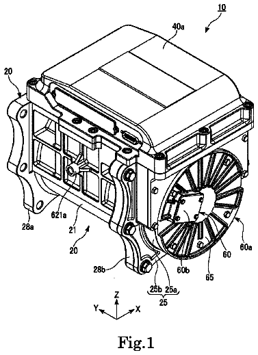
Motor
An object of the present invention is to provide a motor which has a maintenance port and of which the wire is insusceptible to disturbance noise.
US 9,929,636 B2 · Assignee: Mitsubishi Electric Corporation · Inventors: Shinomoto; Yosuke et al.
Sheet 1 of 8 from the published document. All sheets in the USPTO PDF
A first reactor is provided on the input side of a rectifying circuit that rectifies AC power (on the side of an AC power supply), and on the output side of the rectifying circuit (on the side of a load), first and second capacitors that are connected in series to each other, and first and second switching elements that switch between charging and not charging of the first and second capacitors, respectively, are provided, a second capacitor group in Y-connection, provided with three capacitors, each of which is connected to each phase-terminal of the first reactor on the side of the rectifying circuit, is connected to the midpoint of the first and second switching elements, and the output voltage to the load is boosted, while the on-duty of the first switching element and the on-duty of the second switching element are controlled to be equal to each other.
There has been a conventional DC power-supply device, in which a rectifying circuit, connecting rectifying diodes in a full-bridge configuration, rectifies single-phase or three-phase AC commercial power, or the like, and a series-connected switching element group performs switching of the output of the rectifying circuit to store energy in a reactor provided at the previous stage or the subsequent stage of the rectifying circuit, and to charge a capacitor with this energy, which is connected in parallel to the switching element group, thereby supplying a boosted DC voltage to a load. In the DC power-supply device as described above, it is general to change the boost ratio by means of changing the switching, and changing the energy to be stored in the reactor. However, there is a problem that when the switching frequency is increased, a switching loss is increased. To the problem as desc
All 8 drawing sheets from the published document, cropped to the drawing.
What the patent claimed, word for word. All of it is now free to use.
This application is a U.S. national stage application of International Patent Application No. PCT/JP2014/053922 filed on Feb. 19, 2014, the disclosure of which is incorporated herein by reference.
The present invention relates to a DC power-supply device, a motor drive device including the same, and a refrigeration-cycle application device including the motor drive device.
There has been a conventional DC power-supply device, in which a rectifying circuit, connecting rectifying diodes in a full-bridge configuration, rectifies single-phase or three-phase AC commercial power, or the like, and a series-connected switching element group performs switching of the output of the rectifying circuit to store energy in a reactor provided at the previous stage or the subsequent stage of the rectifying circuit, and to charge a capacitor with this energy, which is connected in parallel to the switching element group, thereby supplying a boosted DC voltage to a load. In the DC power-supply device as described above, it is general to change the boost ratio by means of changing the switching, and changing the energy to be stored in the reactor. However, there is a problem that when the switching frequency is increased, a switching loss is increased.
To the problem as described above, a technique to change the boost ratio without changing the switching frequency has been disclosed in Patent Literature 1 listed below, for example. In this technique, in the case of decreasing the boost ratio, a first switching element and a second switching element are turned on/off simultaneously. Also, in the case of increasing the boost ratio, a state transition is repeated, in which the first switching element and the second switching element are turned on simultaneously, one of the switching elements is only turned on, the first and second switching elements are turned on simultaneously, and the other switching element is only turned on.
Patent Literatures 2 and 3 listed below disclose a technique to control an input current into a sine waveform. These Patent Literatures are mentioned later in the descriptions of the embodiments of the present invention.
Patent Literature 1: Japanese Patent Application Laid-open No. 2009-50109
Patent Literature 2: Japanese Patent Application Laid-open No.
H11-168885
Patent Literature 3: Japanese Patent Application Laid-open No. 2009-112172
In the technique in Patent Literature 1 mentioned above, a high boost ratio can be obtained without increasing the switching frequency. However, there is a problem that the switching control method needs to be changed according to whether the boost ratio is decreased or increased, which complicates the control.
The present invention has been achieved to solve the above problems, and an object of the present invention is to provide a DC power-supply device that can more efficiently achieve a high boost ratio with an easier control, a motor drive device including the DC power-supply device, and a refrigeration-cycle application device including the motor drive device.
In order to solve the above-mentioned problems and achieve the object, according to an aspect of the present invention, there is provided a DC power-supply device that converts an alternating current supplied from an AC power supply to a direct current, and that supplies the direct current to a load, the DC power-supply device including: a rectifying circuit that rectifies the alternating current; a first reactor that is inserted between the AC power supply and the rectifying circuit for each phase; a first capacitor group that is provided with a first capacitor and a second capacitor connected in series to each other, and that is connected between output terminals to the load; a switching element group that is provided with a first switching element and a second switching element connected in series to each other, and that is connected in parallel to between the rectifying circuit and the first capacitor group; a backflow prevention unit that prevents a backflow of electric charge to the switching element group, where the electric charge is stored in the first capacitor group by an operation of the switching element group; a second capacitor group that is provided with three capacitors, in each of which one end is electrically connected to a midpoint of the switching element group, and the other end is connected to each phase-terminal of the first reactor on a side of the rectifying circuit; and a second reactor in which one end is connected to a connection point of the first reactor and the second capacitor group, and the other end is connected to the rectifying circuit, wherein the DC power-supply device boosts an output voltage to the load, while controlling an on-duty of the first switching element, and an on-duty of the second switching element to be equal to each other, and an inductance value of the second reactor is smaller than an inductance value of the first reactor.
According to the present invention, it is possible to more efficiently achieve a high boost ratio with an easier control.
FIG. 1 is a diagram illustrating a configuration example of a DC power-supply device according to a first embodiment.
FIG. 2 is a diagram illustrating a switching control state in the DC power-supply device according to the first embodiment.
FIG. 3 is a diagram illustrating each operating mode of the DC power-supply device according to the first embodiment.
FIG. 4 are diagrams illustrating a waveform of each section when the DC power-supply device according to the first embodiment executes a high-frequency switching control.
FIG. 5 is a diagram illustrating a configuration example of a DC power-supply device according to a second embodiment.
FIG. 6 is a diagram illustrating a configuration example of a DC power-supply device according to a third embodiment.
FIG. 7 is a diagram illustrating a configuration example of a motor drive device according to a fourth embodiment, to which an inverter that drives a motor is connected as a load of a DC power-supply device.
FIG. 8 is a diagram illustrating a configuration example of a refrigeration-cycle application device according to the fourth embodiment, to which an inverter that drives a motor of a compressor that constitutes a refrigeration-cycle device is connected as a load of the DC power-supply device.
FIG. 9 is a diagram illustrating a relation between a motor rotational speed and a DC voltage in the motor drive device according to the fourth embodiment.
Exemplary embodiments of a DC power-supply device, a motor drive device including the same, and a refrigeration-cycle application device including the motor drive device according to the present invention will be explained below in detail with reference to the accompanying drawings. The present invention is not limited to the embodiments. First Embodiment
FIG. 1 is a diagram illustrating a configuration example of a DC power-supply device according to a first embodiment. As illustrated in FIG. 1 , a DC power-supply device 100 according to the first embodiment is configured to convert a three-phase alternating current supplied from an AC power supply 1 to a direct current, and supply the direct current to a load 11 according to the operating state of the load 11 . In the present embodiment, a load of an inverter that drives a motor of a compressor used in a refrigeration-cycle device is assumed as the load 11 , for example. However, it is apparent that the load 11 is not limited thereto.
The DC power-supply device 100 includes a rectifying circuit 2 that rectifies a three-phase alternating current, a first reactor 3 on the side of the AC power supply 1 , and a second reactor 8 on the side of the rectifying circuit 2 , each of which is provided at the previous stage of the rectifying circuit 2 , and is inserted between the AC power supply 1 and the rectifying circuit 2 for each phase of the three-phase alternating current, a first capacitor 6 a and a second capacitor 6 b that are connected in series to each other between the output terminals to the load 11 , a first switching element 4 a and a second switching element 4 b that are connected in series to each other between the output terminals of the rectifying circuit 2 , where the first switching element 4 a serves as a first switching unit that switches between charging and not charging of the first capacitor 6 a , and the second switching element 4 b serves as a second switching unit that switches between charging and not charging of the second capacitor 6 b , a first backflow prevention element 5 a that serves as a first backflow prevention unit that prevents a backflow of electric charge stored in the first capacitor 6 a to the first switching element 4 a , a second backflow prevention element 5 b that serves as a second backflow prevention unit that prevents a backflow of electric charge stored in the second capacitor 6 b to the second switching element 4 b , a capacitor group 9 in star connection (in Y-connection) such that one end is connected to each phase, and the other end is connected between the midpoint of the first switching element 4 a and the second switching element 4 b , and the midpoint of the first reactor 3 and the second reactor 8 for each phase, a power-supply voltage detection unit 13 that detects a voltage of the three-phase alternating current, a DC-voltage detection unit 14 that detects a DC voltage to be supplied to the load 11 , and a control unit 12 that controls the first switching element 4 a and the second switching element 4 b . In the example illustrated in FIG. 1 , the rectifying circuit 2 is configured as a three-phase full-wave rectifying circuit, in which six rectifying diodes are connected in a full-bridge configuration. Further, in the example illustrated in FIG. 1 , the power-supply voltage detection unit 13 detects the line voltage between two phases (an r-phase and an s-phase in this example) of the three-phase alternating current supplied from the AC power supply 1 .
The first switching element 4 a and the second switching element 4 b constitute a switching element group. The first backflow prevention element 5 a and the second backflow prevention element 5 b constitute a backflow prevention unit. Further, the first switching element 4 a , the second switching element 4 b , the first backflow prevention element 5 a , and the second backflow prevention element 5 b constitute a charging unit 7 that charges the first capacitor 6 a and the second capacitor 6 b . Furthermore, the first capacitor 6 a and the second capacitor 6 b constitute a first capacitor group. The capacitor group 9 constitutes a second capacitor group. The Y-connection terminals in the capacitor group 9 are not necessarily connected directly to the midpoint of the switching element group. It is also possible that the Y-connection terminals are configured to be electrically connected to the midpoint of the switching element group.
The first capacitor 6 a and the second capacitor 6 b which have the same capacitance are used. As the first switching element 4 a and the second switching element 4 b , a semiconductor element is used, such as a power transistor, a power MOSFET, or an IGBT.
The control unit 12 outputs respective PWM signals SW 1 and SW 2 according to the operating state of the load 11 , and controls the first switching element 4 a and the second switching element 4 b to be on/off, thereby controlling the DC voltage to be supplied to the load 11 . For example, in the case where the load 11 is a motor and an inverter that drives the motor, the operating state of the load 11 is a parameter represented as a rotational speed of the motor, or as an output voltage to be output to the inverter that drives the motor. It is also possible that the control unit 12 is configured to control this load 11 , or another control unit (not illustrated) different from the control unit 12 is configured to control the load 11 . In the case where the control unit 12 is configured to control the load 11 , the control unit 12 is capable of identifying the operating state of the load 11 . In the case where another control unit (not illustrated) different from the control unit 12 is configured to control the load 11 , this different control unit notifies the control unit 12 of the operating state of the load 11 , and then the control unit 12 is capable of identifying the operating state of the load 11 . The present invention is not limited by the method for the control unit 12 to identify the operating state of the load 11 .
Next, a switching control to be executed on the first switching element 4 a and the second switching element 4 b by the control unit 12 is described with reference to FIGS. 1 to 3 . FIG. 2 is a diagram illustrating a switching control state in the DC power-supply device according to the first embodiment. In the example illustrated in FIG. 2 , the reference sign of each constituent element is omitted. FIG. 3 is a diagram illustrating each operating mode of the DC power-supply device according to the first embodiment.
First, with reference to FIG. 2 , the switching control state of the first switching element 4 a and the second switching element 4 b is described.
A state A indicates that the first switching element 4 a and the second switching element 4 b are both controlled to an off state. In this state, the first capacitor 6 a and the second capacitor 6 b are charged.
A state B indicates that only the first switching element 4 a is controlled to an on state. In this state, the second capacitor 6 b is charged.
A state C indicates that only the second switching element 4 b is controlled to an on state. In this state, the first capacitor 6 a is charged.
A state D indicates a short-circuit state, in which two switching elements 4 a and 4 b are both controlled to be on. In this state, basically both the first capacitor 6 a and the second capacitor 6 b are not charged.
According to the operating state of the load 11 , the control unit 12 appropriately switches between the respective states illustrated in FIG. 2 thereby controlling the DC voltage to be supplied to the load 11 .
Next, the operating mode of the DC power-supply device 100 according to the first embodiment is described with reference to FIG. 3 .
As illustrated in FIG. 3 , as the operating mode of the DC power-supply device 100 according to the first embodiment, the DC power-supply device 100 has a full-wave rectification mode, in which the first switching element 4 a and the second switching element 4 b are controlled to a normally off state, and three boost modes, in which the first switching element 4 a and the second switching element 4 b are alternately controlled to be on.
These boost modes are a boost mode “a” (a double-voltage mode), a boost mode “b”, and a boost mode “c”. In the boost mode “a”, the on-duty of the first switching element 4 a and the second switching element 4 b (also referred to as “time ratio” that is the ratio of time, during which each switching element is turned on, relative to the switching cycle) is 50%. In the boost mode “b”, the on-duty of the first switching element 4 a and the second switching element 4 b is less than 50%. In the boost mode “c”, the on-duty of the first switching element 4 a and the second switching element 4 b is greater than 50%.
In the full-wave rectification mode, the first switching element 4 a and the second switching element 4 b are controlled to a normally off state. Therefore, a voltage that is full-wave rectified by the rectifying circuit 2 is an output voltage.
In the boost mode “a” (the double-voltage mode), the first switching element 4 a is turned on and the second switching element 4 b is turned off almost at the same timing. Also, the first switching element 4 a is turned off and the second switching element 4 b is turned on almost at the same timing. The state B and the state C illustrated in FIG. 2 are repeated. At this time, the output voltage is substantially twice as high as the output voltage in the full-wave rectification mode. When the first switching element 4 a and the second switching element 4 b are turned on simultaneously, a short-circuit current flows through these switching elements in practice. Therefore, it is desirable to set several microseconds of dead time.
In the boost mode “b”, a simultaneous off period is set, during which the first switching element 4 a and the second switching element 4 b are both turned off. At this time, a state transition C.fwdarw.A.fwdarw.B.fwdarw.A illustrated in FIG. 2 is periodically repeated. The output voltage at this time is an intermediate voltage between the output voltage in the full-wave rectification mode and the output voltage in the boost mode “a” (the double-voltage mode).
In the boost mode “c”, a simultaneous on period is set, during which the first switching element 4 a and the second switching element 4 b are both turned on. At this time, a state transition D.fwdarw.C.fwdarw.D.fwdarw.B illustrated in FIG. 2 is periodically repeated. During this simultaneous on period (during the period of the state D in this example), energy is stored in the first reactor 3 and the second reactor 8 . At this time, the output voltage becomes equal to or higher than the output voltage in the boost mode “a” (the double-voltage mode).
Therefore, the magnitude relation between the output voltages in the respective modes is expressed as full-wave rectification mode<boost mode “b”<boost mode “a” (double-voltage mode)<boost mode “c”.
As described above, in the present embodiment, it is possible to control the DC voltage to be supplied to the load 11 by means of changing the on-duty of the first switching element 4 a and the second switching element 4 b . According to the operating state of the load 11 , the control unit 12 changes the on-duty of the first switching element 4 a and the second switching element 4 b , thereby shifting the operating mode between the full-wave rectification mode, the boost mode “b”, the boost mode “a” (the double-voltage mode), and the boost mode “c”, and outputting a desired output voltage to the load 11 .
Further, in the present embodiment, as illustrated in FIG. 3 , the control unit 12 executes control such that an on-duty d 1 of the first switching element 4 a matches an on-duty d 2 of the second switching element 4 b in each of the boost modes “a”, “b”, and “c” (d 1 =d 2 ). Due to this control, the processing load on the control unit 12 can be reduced, and therefore the control unit 12 can be implemented by a general low-cost microcomputer. This also facilitates incorporating of the functions of the control unit 12 into a control unit (not illustrated) that controls the load 11 .
That is, in the DC power-supply device 100 according to the present embodiment, by matching the on-duty of the first switching element 4 a and the on-duty of the second switching element 4 b , and also changing this on-duty, a DC voltage twice as high as the power-supply voltage, or even higher can be obtained easily with a low-cost configuration.
Next, the operation of the DC power-supply device 100 according to the first embodiment in each boost mode is described with reference to FIGS. 1 to 4 .
In the present embodiment, as illustrated in FIG. 1 , the DC power-supply device 100 is provided with the power-supply voltage detection unit 13 that detects a three-phase AC voltage, and the DC-voltage detection unit 14 that detects a DC voltage to be supplied to the load 11 . In the example illustrated in FIG. 1 , the power-supply voltage detection unit 13 is configured to detect the line voltage between the r-phase and the s-phase of the three-phase alternating current. However, it is also possible that the power-supply voltage detection unit 13 is configured to detect the line voltage between the s-phase and the t-phase, or between the t-phase and the r-phase, or is configured to detect each phase voltage. The present invention is not limited by the configuration of this power-supply voltage detection unit 13 .
The control unit 12 changes the on-duty of the first switching element 4 a and the second switching element 4 b in each boost mode according to the detected voltage value of the three-phase AC obtained from the detection result of the power-supply voltage detection unit 13 .
The control unit 12 holds the three-phase AC reference voltage value as a threshold value, such that at this reference voltage value, the DC power-supply device 100 is operated in the boost mode “a” (the double-voltage mode), in which the on-duty of the first switching element 4 a and the second switching element 4 b illustrated in FIG. 3 is 50%, for example. When the detected voltage value is smaller than the reference voltage value, the DC power-supply device 100 is operated in the boost mode “c”, in which the on-duty of the first switching element 4 a and the second switching element 4 b is equal to or greater than 50%. When the detected voltage value is greater than the reference voltage value, the DC power-supply device 100 is operated in the boost mode “b”, in which the on-duty of the first switching element 4 a and the second switching element 4 b is less than 50%.
For another example, it is also possible that the control unit 12 holds a table of the on-duty of the first switching element 4 a and the second switching element 4 b such that the output voltage is constant with respect to the detected voltage value of the three-phase AC, and applies the on-duty of the first switching element 4 a and the second switching element 4 b according to the detected voltage value of the three-phase AC.
With the configuration as described above, the variations in three-phase AC voltage can be absorbed, and therefore the output voltage to the load 11 can be stabilized.
In the present embodiment, the DC power-supply device 100 executes a high-frequency switching control, in which the first switching element 4 a and the second switching element 4 b are controlled to be on/off at a switching frequency higher than the power-supply frequency of the AC power supply 1 . FIG. 4 are diagrams illustrating a waveform of each section when the DC power-supply device according to the first embodiment executes a high-frequency switching control. FIG. 4( a ) illustrates an input-voltage waveform from the AC power supply 1 . FIG. 4( b ) illustrates an input-current waveform from the AC power supply 1 . FIG. 4( c ) illustrates a waveform of a neutral-conductor current “i” in which its positive flow direction is from the capacitor group 9 toward the midpoint of the series circuit consisting of the first switching element 4 a and the second switching element 4 b . FIG. 4( d ) illustrates a waveform of a current that flows through the second reactor 8 of the r-phase.
When the second switching element 4 b is controlled to be on, a positive neutral-conductor current “i” flows through the capacitor group 9 , the second switching element 4 b , the rectifying circuit 2 , and the second reactor 8 . In a phase in which the input voltage has a positive polarity, the current (the input current) that flows through the first reactor 3 is increased because the neutral-conductor current “i” is supplied from the side of the AC power supply 1 , and then flows into the capacitor group 9 . In contrast, in a phase in which the input voltage has a negative polarity, the input current is decreased because the neutral-conductor current “i” flows from the second reactor 8 into the capacitor group 9 , and therefore does not flow out to the side of the AC power supply 1 .
Further, when the first switching element 4 a is controlled to be on, a negative neutral-conductor current “i” flows through the second reactor 8 , the rectifying circuit 2 , the first switching element 4 a , and the capacitor group 9 . In a phase in which the input voltage has a positive polarity, the current (the input current) that flows through the first reactor 3 is decreased because the neutral-conductor current “i” flows from the capacitor group 9 to the second reactor 8 . In contrast, in a phase in which the input voltage has a negative polarity, the input current is increased because the neutral-conductor current “i” flows out from the capacitor group 9 to the AC power supply 1 .
The switching operations described above are summarized in the following table.
TABLE-US-00001 TABLE 1 Input current Positive Negative First switching element 4a = ON Decrease Increase Second switching element 4b = ON Increase Decrease
As described above, the increase and decrease in input current for each phase can be controlled by controlling the first switching element 4 a and the second switching element 4 b to be on/off alternately. Therefore, the input current flows according to the input voltage for each phase. In the case where the AC power supply 1 is a three-phase AC power supply, the input currents that respectively flow through the three phases are balanced, and accordingly the DC power-supply device is capable of operating in a stable manner. The term “alternately” does not always mean that when one switching element (the first switching element 4 a , for example) is controlled to be on, the other switching element (the second switching element 4 b , for example) needs to be off. It is permissible that there is a period during which the switching elements are simultaneously turned on. For example, it suffices that the first switching element 4 a and the second switching element 4 b are controlled at the same on-duty (including substantially the same on-duty), and additionally there is a time slot in which when one switching element is controlled to be on, the other switching element is controlled to be off as the periods B and C in the boost mode “c” illustrated in FIG. 3 . The same applies to the following descriptions.
Next, the reasons why it is possible to control the input current into a sine waveform are described. The DC power-supply device 100 of the present application includes the first reactor 3 and the second reactor 8 . To their connection point, the capacitor group 9 is connected. When the inductance value (L 8 ) of the second reactor 8 is set smaller than the inductance value (L 3 ) of the first reactor 3 (that is, L 3 >L 8 ), a current can flow through the second reactor 8 in a discontinuous mode. It is sufficient to set L 3 >L 8 , and therefore even where L 8 =0 is established, that is, even when the DC power-supply device 100 does not include a second reactor, it still functions as a DC power-supply device that boosts the voltage, although some degree of distortion appears in the input current waveform. In this sense, an embodiment, in which the DC power-supply device does not include a second reactor, also constitutes the scope of the present embodiment. However, it is apparent that parasitic inductance components attributable to the wiring or the like are present in practice.
When a current flows in a discontinuous mode, the current peak is so high that a significant amount of noise is emitted to the AC power supply 1 . However, because the first reactor 3 is located in front of the connection point with the AC power supply 1 , the impedance can be increased at the first reactor 3 . When the switching is performed in a discontinuous mode, the current has the same waveform as that of the AC power supply 1 , and the waveform can be improved to a sine waveform. Because the DC power-supply device 100 is provided with the first reactor 3 in front of the connection point with the AC power supply 1 , an input current with a continuous sine waveform flows due to the current rectification effect of the first reactor 3 . FIG. 4 are waveform diagrams of the analysis results. It can be also understood from FIG. 4 that a discontinuous-mode current (d) in the second reactor 8 has been improved to a sine waveform with a continuous shape in the input current (b).
As described above, the waveform of all the three-phase input currents can be improved to a sine waveform by only turning on/off the first switching element 4 a and the second switching element 4 b alternately. Therefore, power-factor improvement and harmonic-current suppression can both be achieved. Further, because the waveform of an input current can be improved to a sine waveform, a harmonic current can be greatly reduced, and suppressed to a state where the harmonic current is very close to zero. The power factor of the power supply can be also improved to approximately 100%.
When the first switching element 4 a and the second switching element 4 b are controlled to be on/off alternately, a current flows through the second reactor 8 in a discontinuous mode, and a combined current of the second reactor 8 for each phase is output from the rectifying circuit 2 . Not only this current becomes a neutral-conductor current through the first switching element 4 a or the second switching element 4 b , but also this current is charged into the capacitors 6 a and 6 b through the backflow prevention elements 5 a and 5 b , respectively.
The midpoint of the first capacitor 6 a and the second capacitor 6 b , and the midpoint of the first switching element 4 a and the second switching element 4 b are at equal potential. This potential is also equal to the potential at the connection point of the capacitor group 9 . Therefore, the voltage is changed with ripples in the carrier cycle. With this voltage change, the first capacitor 6 a and the second capacitor 6 b are charged. Accordingly, the electric charge is replenished in the first capacitor 6 a and the second capacitor 6 b per carrier cycle. Consequently, based on the double voltage rectification, the amount of charge to the capacitor is increased by high-frequency switching in a discontinuous mode. DC-voltage boosting can be thus achieved.
In a general high-frequency switching DC power-supply device, the DC voltage is boosted by a factor of “power-supply-voltage effective value” ×√2×1.3 to 1.4. In the DC power-supply device of the present application, based on the double voltage rectification, the DC voltage is boosted by a factor of “power-supply-voltage effective value” ×2×√2×1.3 to 1.4 by solely turning on/off two switching elements. The voltage boosting can be achieved twice as much as the general technique.
In the manner as described above, the DC voltage can be boosted twice as high as the power-supply voltage under the condition with the same switching loss as the general DC power-supply device. Assuming that the voltage is boosted to the same level as the general DC power-supply device, the DC power-supply device of the present application is capable of boosting the voltage at a lower loss than the conventional technique in which the switching elements are alternately turned on/off by general high-frequency switching (for example, Patent Literature 2 and Patent Literature 3).
It is obvious that by adjusting the duty cycle for turning the switching elements on/off alternately, the DC power-supply device of the present application can adjust the voltage to be boosted. Furthermore, based on the double voltage, the DC power-supply device of the present application can widely control the adjustment range of the voltage to be boosted. Because the DC power-supply device of the present application turns on/off the switching elements alternately at a high frequency, the first capacitor 6 a and the second capacitor 6 b are charged at a high frequency, and therefore their capacitance can be reduced. The first capacitor 6 a and the second capacitor 6 b can be implemented by downsized capacitors.
As described above, in the DC power-supply device according to the first embodiment, a first reactor is provided on the input side of a rectifying circuit that rectifies AC power (on the power-supply side), and on the output side of the rectifying circuit (on the load side), a first capacitor and a second capacitor that are connected in series to each other, and a first switching element and a second switching element that switch between charging and not charging of the first capacitor and the second capacitor, respectively, are provided. In this configuration, a second capacitor group in Y-connection, provided with three capacitors, each of which is connected to each phase-terminal of the first reactor on the side of the rectifying circuit, is connected to the midpoint of the first switching element and the second switching element, and the output voltage to the load is boosted, while the on-duty of the first switching element, and the on-duty of the second switching element are controlled to be equal to each other. Therefore, even when a DC voltage twice as high as the power-supply voltage, or even higher is obtained, the input-current waveform for each phase can still be shaped into a sine waveform easily with a low-cost configuration. Accordingly, it is possible to improve the power factor of the power supply, and decrease a harmonic current.
Further, the DC power-supply device can be operated at a higher boost ratio by easily controlling the on-duty without complicating the switching control. Even when the DC power-supply device is operated at a higher boost ratio, a switching loss can still be suppressed. Therefore, it is possible to achieve high efficiency.
Furthermore, it is possible to expand the adjustment range of the output voltage by changing the on-duty of the first switching unit and the second switching unit. Furthermore, it is possible to achieve a reduction in capacitance of the first capacitor and the second capacitor by executing a high-frequency switching control. Second Embodiment
FIG. 5 is a diagram illustrating a configuration example of a DC power-supply device according to a second embodiment. Constituent elements identical or equivalent to those in the first embodiment are denoted by like reference signs and detailed descriptions thereof will be omitted.
In a DC power-supply device 100 a according to the present embodiment illustrated in FIG. 5 , the first reactor 3 and the second reactor 8 in the configuration illustrated in FIG. 1 and described in the first embodiment are magnetically coupled together to form a magnetically-coupled reactor. Reactors 50 , 51 , and 52 that are provided for the respective phases are configured as the magnetically-coupled reactors.
Due to the configuration as described above, the spatial volume of the reactors can be reduced in configuring the DC power-supply device 100 a . Particularly, in the form of providing a center tap that is connected from the reactors 50 , 51 , and 52 to the capacitor group 9 , the reactors 50 , 51 , and 52 can be configured as a single component structurally. Accordingly, it is possible to achieve spatial volumetric efficiency. Further, the same magnetically-coupled reactors for three phases are used, and therefore at the time of manufacturing the device, a cost reduction can be expected due to an increased number of the same reactors used.
As described in the first embodiment, it is necessary to set the inductance value of the second reactor 8 smaller than the inductance value of the first reactor 3 . Specifically, upon performing high-frequency switching, the second reactor 8 needs to pass a discontinuous-mode current including many harmonic components, that is, many noise components. The first reactor 3 filters the noise components so as to shape the input current into a continuous sine waveform, and therefore needs dependency of the inductance capacitance on the current. Accordingly, a core material with high frequency characteristics is preferable as a core material of the second reactor 8 . Also, a core material with a high magnetic density is preferable as a core material of the first reactor 3 .
As described above, the first reactor 3 and the second reactor 8 are made of different core materials, and are magnetically coupled together. Therefore, DC components of the currents that flow respectively through the reactors 3 and 8 can be cancelled each other out, and DC excitation is cancelled. Accordingly, current saturation can be suppressed. Due to this configuration, the magnetically coupled reactors of the first reactor 3 and the second reactor 8 can achieve higher spatial volumetric efficiency than that of the simple magnetically-coupled reactors that share the iron core.
As described above, in the DC power-supply device according to the second embodiment, a first reactor and a second reactor for each phase are configured by a single magnetically-coupled reactor, thereby reducing the spatial volume of the reactor in configuring the DC power-supply device. Further, the same magnetically-coupled reactors for three phases are used, and therefore at the time of manufacturing the device, a cost reduction can be expected due to an increased number of the same reactors used.
Furthermore, the first reactor and the second reactor are made of different core materials, and magnetically coupled together. Therefore, the DC components of the currents that flow respectively through the reactors are cancelled each other out, and DC excitation is cancelled. Accordingly, current saturation can be suppressed. Consequently, the magnetically coupled reactors of the first reactor and the second reactor can achieve higher spatial volumetric efficiency than that of the simple magnetically-coupled reactors that share the iron core. Third Embodiment
FIG. 6 is a diagram illustrating a configuration example of a DC power-supply device according to a third embodiment. Constituent elements identical or equivalent to those in the first embodiment are denoted by like reference signs and detailed descriptions thereof will be omitted.
As illustrated in FIG. 6 , in a DC power-supply device 100 b according to the third embodiment, in addition to the configuration illustrated in FIG. 1 and described in the first embodiment, the midpoint of the series circuit consisting of the first switching element 4 a and the second switching element 4 b , and the midpoint of the series circuit consisting of the first capacitor 6 a and the second capacitor 6 b , are connected to each other through an opening-closing unit 20 that is a neutral-conductor disconnection unit.
In the configuration of the first and second embodiments in which the opening-closing unit 20 is not included, when the DC power-supply device continues the operation in a state where a fault has occurred in any of the first backflow prevention element 5 a , the second backflow prevention element 5 b , the first switching element 4 a , and the second switching element 4 b , voltage unbalance between the first capacitor 6 a and the second capacitor 6 b is caused and the voltage of the first capacitor 6 a and the second capacitor 6 b may exceed their withstand voltage, resulting in a secondary fault. In order to prevent the secondary fault as described above, it is necessary to stop the operation of the device connected as the load 11 to the DC power-supply device.
In the present embodiment, the DC power-supply device 100 b is provided with the opening-closing unit 20 . Therefore, in a case where a short-circuit fault has occurred in any of the first backflow prevention element 5 a , the second backflow prevention element 5 b , the first switching element 4 a , and the second switching element 4 b , the opening-closing unit 20 is controlled to be opened, and also the DC power-supply device 100 b is operated in the full-wave rectification mode. This makes it possible to supply power to the load 11 in a stable manner without causing voltage unbalance between the first capacitor 6 a and the second capacitor 6 b . It is also possible to continue the operation of the device connected as the load 11 to the DC power-supply device 100 b.
The description continues in the full USPTO document.
About 6,824 words. The USPTO PDF has it with every drawing.
Fees are due 3.5, 7.5 and 11.5 years after grant. This patent expired on March 27, 2026, so the fee marked "not paid" was the one that went unpaid.
DC POWER-SUPPLY DEVICE, MOTOR DRIVE DEVICE INCLUDING THE SAME, AND REFRIGERATION-CYCLE APPLICATION DEVICE INCLUDING THE MOTOR DRIVE DEVICE
Filed Feb 2014 · published Jan 2017DC power-supply device, motor drive device including the same, and refrigeration-cycle application device including the motor drive device
Filed Feb 2014 · granted Mar 2018Earlier publications, parents and continuations. None of them can still be enforced, or this patent would not be listed.
Prior art cited by the examiner or applicant. Useful when you check your own idea for novelty.
Everything on this page comes from the documents linked above.