Lapsed, fee not paid11 drawings
Chips & Semiconductors · US 9,929,268 B2
Fin field effect transistor and method for fabricating the same
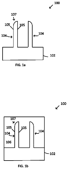
A method of fabricating a FinFET includes at last the following steps.
US 9,929,303 B2 · Assignee: CANON KABUSHIKI KAISHA · Inventors: Kanesada; Takayasu
Sheet 1 of 9 from the published document. All sheets in the USPTO PDF
A method of manufacturing a solid-state image sensor is provided. A first insulating member and an electrically conductive member is formed above a semiconductor substrate. A connecting portion of an upper surface of the electrically conductive member is covered with part of the first insulating member. First openings corresponding to the photoelectric conversion units are formed in the first insulating member. A second insulating member covering the first insulating member is then formed. The second insulating member is partially removed to expose the part of the first insulating member covering the connecting portion. A third insulating member that covers the first and second insulating members is then formed. The third insulating member is partially removed to expose the second insulating member. A second opening to expose the connecting portion is then formed to form a plug.
8 of 9 drawing sheets so far from the published document, cropped to the drawing. Every sheet is in the USPTO PDF.
What the patent claimed, word for word. All of it is now free to use.
BACKGROUND OF THE INVENTION Field of the Invention
The present invention relates to a method of manufacturing a solid-state image sensor. Description of the Related Art
There is proposed a solid-state image sensor including a light waveguide to increase the amount of light entering a photoelectric conversion unit. In Japanese Patent Laid-Open Nos. 2012-164945 and 2014-036036, an opening is formed in an insulating member of a low refractive index, and an insulating member of a high refractive index is formed on this insulating member. A portion of the insulating member of the high refractive index arranged in the opening forms the core of a light waveguide. The insulating member of the high refractive index is formed not only on the pixel region but also on the peripheral region. If the insulating member of the high refractive index remains when forming a plug in the peripheral region, it is difficult to form a through hole used to arrange the plug. Hence, in Japanese Patent Laid-Open Nos. 2012-164945 and 2014-036036, the through hole is formed after the portion of the insulating member of the high refractive index arranged on the peripheral region is removed.
In Japanese Patent Laid-Open Nos. 2012-164945 and 2014-036036, only the portion of the insulating member of the high refractive index located on the peripheral region is removed. For this reason, a step is generated on the upper surface of the insulating member. Because of this step, planarization of the upper surface of an insulating film formed later may be insufficient, or the solid-state image sensor may become tall. As a result, image quality obtained by the solid-state image sensor lowers. An aspect of the present invention provides a technique for reducing a step generated on the upper surface of an insulating member used to form a light waveguide.
According to some embodiments, a method of manufacturing a solid-state image sensor is provided. The method includes: forming a first insulating member and an electrically conductive member above a semiconductor substrate including a first region in which a plurality of photoelectric conversion units are arranged and a second region in which a circuit configured to process signals from the plurality of photoelectric conversion units is arranged, wherein the first insulating member covers the first region and the second region, the electrically conductive member is arranged above at least the second region, and a connecting portion of an upper surface of the electrically conductive member, which is used to connect a plug, is covered with part of the first insulating member; forming a plurality of first openings corresponding to the plurality of photoelectric conversion units in the first insulating member; forming a second insulating member above the first region and the second region after the forming the plurality of first openings, wherein the second insulating member covers the first insulating member, and a portion of the second insulating member formed in the first opening functions as a waveguide; partially removing the second insulating member such that the part of the first insulating member covering the connecting portion is exposed; forming a third insulating member that covers the first insulating member and the second insulating member above the first region and the second region after the partially removing the second insulating member; partially removing the third insulating member formed above the first region such that the second insulating member is exposed; forming a second opening to expose the connecting portion of the electrically conductive member in the first insulating member and the third insulating member after the partially removing the third insulating member; and forming the plug in the second opening.
Further features of the present invention will become apparent from the following description of exemplary embodiments (with reference to the attached drawings).
FIGS. 1A to 1C are views for explaining a solid-state image sensor manufacturing method according to some embodiments;
FIGS. 2A to 2C are views for explaining a solid-state image sensor manufacturing method according to some embodiments;
FIGS. 3A to 3C are views for explaining a solid-state image sensor manufacturing method according to some embodiments;
FIGS. 4A to 4C are views for explaining a solid-state image sensor manufacturing method according to some embodiments;
FIG. 5 is a view for explaining a solid-state image sensor manufacturing method according to some embodiments;
FIGS. 6A to 6C are views for explaining a solid-state image sensor manufacturing method according to some embodiments;
FIGS. 7A to 7C are views for explaining a solid-state image sensor manufacturing method according to some embodiments;
FIGS. 8A to 8C are views for explaining a modification of the solid-state image sensor manufacturing method; and
FIGS. 9A to 9C are views for explaining a modification of the solid-state image sensor manufacturing method.
Embodiments of the present invention will now be described with reference to the accompanying drawings. The same reference numerals denote the same elements throughout various embodiments, and a repetitive description thereof will be omitted. The embodiments can appropriately be changed or combined. In the following explanation, a case in which signal charges are electrons will be described. However, the signal charges may be holes. If the signal charges are holes, the conductivity types of semiconductor regions to be described below are replaced. First Embodiment
A method of manufacturing a solid-state image sensor according to the first embodiment of the present invention will be described with reference to the accompanying drawings. FIGS. 1A to 4C are schematic views of the sectional structure of a solid-state image sensor in the steps according to this embodiment. In each step, the solid-state image sensor halfway through the manufacture will also be referred to as a solid-state image sensor 100 .
First, a semiconductor substrate 101 of the solid-state image sensor 100 is prepared. The semiconductor substrate 101 is a semiconductor material portion of members that constitute the solid-state image sensor 100 . For example, the semiconductor substrate 101 includes a semiconductor wafer in which a semiconductor region is formed by a known semiconductor manufacturing process. An example of the semiconductor material is silicon. The interface between the semiconductor material and another material is a principal surface 102 of the semiconductor substrate 101 . Another material is, for example, a thermal oxide film (not shown) that is arranged on the semiconductor substrate 101 and is in contact with the principal surface 102 of the semiconductor substrate 101 .
In this embodiment, a known semiconductor substrate can be used as the semiconductor substrate 101 . A p-type semiconductor region and an n-type semiconductor region are arranged in the semiconductor substrate 101 . The semiconductor substrate 101 includes an imaging region 103 in which a plurality of photoelectric conversion units are arranged, and a peripheral region 104 in which a signal processing circuit configured to process signals from the plurality of photoelectric conversion units is arranged. The imaging region 103 and the peripheral region 104 will be described later.
Note that in this specification, a surface parallel to the principal surface 102 will simply be referred to as a plane. For example, of the principal surface 102 , a portion in which photoelectric conversion units to be described later are arranged, or a portion in the channel of a MOS transistor may be used as a reference for a plane. Additionally, in this specification, a surface intersecting, for example, orthogonal to a plane will simply be referred to as a section.
In the step shown in FIG. 1A , the semiconductor regions are formed in the semiconductor substrate 101 , and gate electrodes and multiple wiring layers are formed on the semiconductor substrate 101 . In the imaging region 103 of the semiconductor substrate 101 , photoelectric conversion units 105 , a floating diffusion (to be referred to as an FD hereinafter) 106 , a well 107 for pixel transistors, and source and drain regions are formed. The photoelectric conversion unit 105 is, for example, a photodiode. The photoelectric conversion unit 105 includes the n-type semiconductor region arranged in the semiconductor substrate 101 . Electrons generated by photoelectric conversion are collected by the n-type semiconductor region of the photoelectric conversion unit 105 . The FD 106 is an n-type semiconductor region. Electrons generated in the photoelectric conversion unit 105 are transferred to the FD 106 and converted into a voltage. The FD 106 is electrically connected to the input node of an amplification portion. Instead, the FD 106 may electrically be connected to a signal output line. In this embodiment, the FD 106 is electrically connected a gate electrode 110 b of an amplification transistor via a plug 114 . The source and drain regions of the amplification transistor configured to amplify a signal, a reset transistor configured to reset the input node of the amplification transistor, and the like are formed in the well 107 for pixel transistors.
A well 108 for peripheral transistors is formed in the peripheral region 104 of the semiconductor substrate 101 . The source and drain regions of peripheral transistors that constitute a signal processing circuit are formed in the well 108 for peripheral transistors. An element isolation portion 109 may be formed in the semiconductor substrate 101 . The element isolation portion 109 electrically isolates the pixel transistors or the peripheral transistors from other elements. The element isolation portion 109 is STI (Shallow Trench Isolation), LOCOS (LOCal Oxidation of Silicon), or the like.
Additionally, in this step, a transfer gate electrode 110 a and the gate electrode 110 b are formed. The transfer gate electrode 110 a and the gate electrode 110 b are arranged on an oxide film (not shown) on the semiconductor substrate 101 . The transfer gate electrode 110 a controls charge transfer between the photoelectric conversion unit 105 and the FD 106 . The gate electrode 110 b is the gate of a pixel transistor or a peripheral transistor.
Furthermore, in this step, a protective layer 111 is formed on the semiconductor substrate 101 . The protective layer 111 is, for example, a silicon nitride film. The protective layer 111 may be formed from a plurality of layers including a silicon nitride film and a silicon oxide film. The protective layer 111 may have at least one of a function of reducing damage to the photoelectric conversion units in the subsequent step, a function of preventing reflection, and a function of preventing diffusion of a metal in a silicide process. In addition, an etching stop member 117 is formed on the opposite side of the semiconductor substrate 101 with respect to the protective layer 111 . The area of the etching stop member 117 may be larger than the area of the bottom of an opening 116 to be formed later. Note that the protective layer 111 and the etching stop member 117 need not always be formed. In this specification, an area is the area of a surface parallel to the principal surface 102 , unless specifically stated otherwise. For example, the area of a through hole 125 to be described below is the area of a region on a plane where the through hole 125 is projected onto the plane.
Next, an insulating member and an electrically conductive member are formed on the semiconductor substrate 101 . In this embodiment, the insulating member is formed from a plurality of interlayer dielectric films 113 a to 113 e and insulating films 115 and covers the imaging region 103 and the peripheral region 104 . The plurality of interlayer dielectric films 113 a to 113 e and the insulating films 115 , which constitute the insulating member, will simply be referred to as the interlayer dielectric films 113 and the like hereinafter. The electrically conductive member is formed from a first wiring layer 112 a and a second wiring layer 112 b , and includes at least a portion arranged on the imaging region 103 and a portion arranged on the peripheral region 104 . In this embodiment, the first wiring layer 112 a and the second wiring layer 112 b are formed by a damascene method. For the sake of convenience, the interlayer dielectric films will be referred to as the first to fifth interlayer dielectric films 113 a to 113 e sequentially from the side close to the semiconductor substrate 101 . The first to fifth interlayer dielectric films 113 a to 113 e are formed by, for example, plasma CVD. The film thickness of each interlayer dielectric film may be, for example, 120 nm to 1000 nm. The upper surface of the second wiring layer 112 b includes a portion (to be referred to as a connecting portion hereinafter) used to connect a plug 121 to be described later. The connecting portion of the second wiring layer 112 b is covered with part of the fifth interlayer dielectric film 113 e and the insulating film 115 .
A step of forming the interlayer dielectric films 113 and the like and the electrically conductive member on the semiconductor substrate 101 will be described below in detail. First, the first interlayer dielectric film 113 a is formed on the imaging region 103 and the peripheral region 104 . The surface of the first interlayer dielectric film 113 a on the opposite side of the semiconductor substrate 101 may be planarized as needed. Through holes are formed in the first interlayer dielectric film 113 a . The plug 114 that electrically connects the electrically conductive member of the first wiring layer 112 a and the semiconductor region of the semiconductor substrate 101 is arranged in each through hole. The plug 114 is made of an electrically conductive material. For example, the plug 114 is made of tungsten.
Next, the second interlayer dielectric film 113 b is formed on the opposite side of the semiconductor substrate 101 with respect to the first interlayer dielectric film 113 a . Of the second interlayer dielectric film 113 b , a portion corresponding to the region where the electrically conductive member of the first wiring layer 112 a is arranged is removed by etching. After that, a metal film as the material of the first wiring layer is formed on the imaging region 103 and the peripheral region 104 . Then, the metal film is removed by a method such as CMP until the second interlayer dielectric film is exposed. According to this procedure, the electrically conductive member that forms the wiring of the first wiring layer 112 a is arranged in a predetermined pattern.
Subsequently, the third interlayer dielectric film 113 c and the fourth interlayer dielectric film 113 d are formed on the imaging region 103 and the peripheral region 104 . Of the fourth interlayer dielectric film 113 d , a portion corresponding to the region where the electrically conductive member of the second wiring layer 112 b is arranged is removed by etching. Next, of the third interlayer dielectric film 113 c , a portion corresponding to the region where a plug that electrically connects the electrically conductive member of the first wiring layer 112 a and the electrically conductive member of the second wiring layer 112 b is arranged is removed by etching. After that, a metal film as the material of the second wiring layer and the plug is formed on the imaging region 103 and the peripheral region 104 . Then, the metal film is removed by a method such as CMP until the fourth interlayer dielectric film is exposed. According to this procedure, the wiring pattern of the second wiring layer 112 b and the wiring pattern of the plug are obtained. Note that after the third interlayer dielectric film 113 c and the fourth interlayer dielectric film 113 d are formed, the portion corresponding to the region where the plug that electrically connects the electrically conductive member of the first wiring layer 112 a and the electrically conductive member of the second wiring layer 112 b is arranged may be removed by etching first.
Finally, the fifth interlayer dielectric film 113 e is formed on the imaging region 103 and the peripheral region 104 . The surface of the fifth interlayer dielectric film 113 e on the opposite side of the semiconductor substrate 101 may be planarized by a method such as CMP as needed.
Note that the first wiring layer 112 a and the second wiring layer 112 b may be formed by a method other than the damascene method. An example of a method other than the damascene method will be described. After the first interlayer dielectric film 113 a is formed, a metal film as the material of the first wiring layer is formed on the imaging region 103 and the peripheral region 104 . Next, of the metal film, a portion other than the region where the electrically conductive member of the first wiring layer 112 a is arranged is removed by etching. The wiring pattern of the first wiring layer 112 a is thus obtained. After that, the second interlayer dielectric film 113 b and the third interlayer dielectric film 113 c are formed, and the second wiring layer 112 b is formed in a similar manner. After the second wiring layer 112 b is formed, the fourth interlayer dielectric film 113 d and the fifth interlayer dielectric film 113 e are formed. The surfaces of the third interlayer dielectric film 113 c and the fifth interlayer dielectric film 113 e on the opposite side of the semiconductor substrate 101 may be planarized.
The first wiring layer 112 a and the second wiring layer 112 b are arranged to different heights with respect to the principal surface 102 of the semiconductor substrate 101 as a reference. In this embodiment, the electrically conductive members of the first wiring layer 112 a and the second wiring layer 112 b are made of copper. The electrically conductive members may be made of any conductive material other than copper. Except the portions electrically connected by the plug, the electrically conductive member of the first wiring layer 112 a and the electrically conductive member of the second wiring layer 112 b are insulated from each other by the third interlayer dielectric film 113 c . Note that the number of wiring layers is not limited to 2, and a single wiring layer or three or more layers may be formed.
The insulating film 115 having at least one of the functions of an etching stop film and a metal diffusion preventing film may be arranged between the interlayer dielectric films. In this embodiment, the plurality of interlayer dielectric films 113 a to 113 e are silicon oxide films. A silicon nitride film serves as an etching stop film for a silicon oxide film. The insulating film 115 may be made of silicon carbide or silicon carbonitride. The film thickness of the insulating film 115 may be about 10 nm to 200 nm. Note that the insulating film 115 need not always be arranged.
In the step shown in FIG. 1B , the plurality of openings 116 corresponding to the plurality of photoelectric conversion units 105 are formed in the interlayer dielectric films 113 and the like. The openings 116 are formed such that of the plurality of interlayer dielectric films 113 a to 113 e , portions located on the connecting portion of the second wiring layer 112 b are left. First, an etching mask pattern (not shown) is formed on the opposite side of the semiconductor substrate 101 with respect to the interlayer dielectric film 113 e . The etching mask pattern covers portions other than the regions where the openings 116 should be arranged. In other words, the etching mask pattern has openings in the regions where the openings 116 should be arranged. The etching mask pattern is, for example, a photoresist patterned by photolithography and development.
Next, the plurality of interlayer dielectric films 113 a to 113 e and the insulating films 115 are etched using the etching mask pattern as a mask. The openings 116 are thus formed. The openings 116 may be formed by a plurality of times of etching under different conditions. After the etching, the etching mask pattern may be removed.
When the etching stop member 117 is arranged, etching may be performed in the step of FIG. 1B until the etching stop member 117 is exposed. In the etching condition to etch the interlayer dielectric film 113 a , the etching rate of the etching stop member 117 may be lower than the etching rate of the interlayer dielectric film 113 a . If the interlayer dielectric film 113 a is a silicon oxide film, a silicon nitride film or silicon oxynitride film can be used as the etching stop member 117 . The etching stop member 117 may be exposed by a plurality of times of etching under different conditions.
The opening 116 may extend through only some of the first to fifth interlayer dielectric films 113 a to 113 e . A recess provided in the interlayer dielectric films 113 a to 113 e may be the opening 116 . The planar shape of the opening 116 is a closed loop shape such as a circle or a rectangle. Instead, the planar shape of the opening 116 may be a shape like a trench extending over the plurality of photoelectric conversion units 105 . That is, in this specification, if a region on a certain plane where the interlayer dielectric film 113 e is not arranged is surrounded or sandwiched by regions where the interlayer dielectric film 113 e is arranged, the interlayer dielectric film 113 e has the opening 116 .
The opening 116 is arranged such that at least part of the opening 116 overlaps the insulating photoelectric conversion unit 105 on a plane. That is, if the opening 116 and the photoelectric conversion unit 105 are projected onto the same plane, there exists a region where both the opening 116 and the photoelectric conversion unit 105 are projected on the same plane.
In this embodiment, the openings 116 are formed in a region overlapping the photoelectric conversion units 105 , and no opening 116 is formed on the peripheral region 104 . Instead, the openings 116 may be formed on the peripheral region 104 . In this case, the density of the openings 116 formed on the imaging region 103 may be higher than the density of the openings 116 formed on the peripheral region 104 . The density of the openings 116 can be determined based on the number of openings 116 arranged per unit area. Alternatively, the density of the openings 116 can be determined based on the ratio of the area occupied by the openings 116 per unit area.
Next, another insulating member is formed on the imaging region 103 and the peripheral region 104 of the semiconductor substrate 101 in a series of steps shown in FIGS. 1C to 3A . In this embodiment, this insulating member is formed from a first waveguide member 118 , a second waveguide member 122 , and a low refractive index member 123 . The first waveguide member 118 , the second waveguide member 122 , and the low refractive index member 123 , which constitute the insulating member, will simply be referred to as the first waveguide member 118 and the like. The refractive index of the low refractive index member 123 is lower than the refractive index of the first waveguide member 118 and the second waveguide member 122 . The first waveguide member 118 and the second waveguide member 122 are partially formed in the openings 116 . The low refractive index member 123 is formed above the openings 116 . The first waveguide member 118 and the like cover the interlayer dielectric films 113 and the like. The first waveguide member 118 and the like partially enter the openings 116 , and the portions formed in the openings 116 function as a light waveguide. The first waveguide member 118 and the like may be made of a material different from the interlayer dielectric films 113 and the like. For example, if the first waveguide member 118 and the like and the interlayer dielectric films 113 and the like are in contact with each other, the materials on both sides of the interface may be different from each other.
The series of steps shown in FIGS. 1C to 3A will be described below in detail. The first waveguide member 118 can be formed by deposition based on CVD or sputtering or application of an organic material represented by a polyimide-based polymer. Note that the first waveguide member 118 may be formed in a plurality of steps under different conditions. For example, in the first step, the first waveguide member 118 may be formed under a condition to increase adhesion to an underlying layer. In the next step, the first waveguide member 118 may be formed under a condition to improve the burying characteristic in the openings 116 . Alternatively, the first waveguide member 118 may be formed by sequentially forming a plurality of different materials. For example, the first waveguide member 118 may be formed by depositing a silicon nitride film first and then depositing an organic material of high burying performance. If the first interlayer dielectric film 113 a is etched in the step of FIG. 1B until the etching stop member 117 is exposed, the first waveguide member 118 is arranged in contact with the etching stop member 117 .
The material of the first waveguide member 118 may have a refractive index higher than that of the interlayer dielectric films 113 a to 113 e . If the interlayer dielectric films 113 a to 113 e are silicon oxide films, a silicon nitride film or a polyimide-based organic material can be used as the material of the first waveguide member 118 . The refractive index of the silicon nitride film is about 2.0. The refractive index of the silicon oxide films on the periphery is about 1.4. For this reason, based on the Snell's law, light is reflected by the interface between the first waveguide member 118 and the interlayer dielectric films 113 a to 113 e . This can confine the light in the first waveguide member 118 . In addition, the hydrogen content of the silicon nitride film can be increased, and the dangling bond of the semiconductor substrate 101 can be terminated by the hydrogen supply effect. This can reduce noise such as a white spot defect. The refractive index of the polyimide-based organic material is about 1.7. The burying characteristic of the polyimide-based organic material is better than that of a silicon nitride film. The material of the first waveguide member 118 may appropriately be selected in consideration of the balance between an optical characteristic such as a refractive index difference and an advantage in the manufacturing process.
The positional relationship between the plurality of interlayer dielectric films 113 a to 113 e and the first waveguide member 118 arranged in the opening 116 will be described here. On a given plane, the region where the first waveguide member 118 is arranged is surrounded by or sandwiched between regions where the plurality of interlayer dielectric films 113 a to 113 e are arranged. In other words, first portions of the plurality of interlayer dielectric films 113 a to 113 e , second portions different from the first portions, and the first waveguide member 118 arranged in the opening 116 are aligned in a direction intersecting the direction in which the photoelectric conversion unit 105 and the first waveguide member 118 arranged in the opening 116 are aligned. The direction intersecting the direction in which the photoelectric conversion unit 105 and the first waveguide member 118 arranged in the opening 116 are aligned is, for example, a direction parallel to the principal surface 102 of the semiconductor substrate 101 .
Part of the first waveguide member 118 is arranged at a position overlapping the photoelectric conversion unit 105 on the semiconductor substrate 101 . The peripheral region interlayer dielectric films 113 a to 113 e are arranged around the portion of the first waveguide member 118 . The refractive index of the material of the first waveguide member 118 may be higher than the refractive index of the plurality of interlayer dielectric films 113 a to 113 e . By the refractive index relationship, of light that has entered the first waveguide member 118 , the amount of light leaking to the plurality of interlayer dielectric films 113 a to 113 e can be reduced. For this reason, if at least part of the first waveguide member 118 is arranged while overlapping the photoelectric conversion unit 105 , the amount of light that enters the photoelectric conversion unit 105 can be increased.
The refractive index of the first waveguide member 118 may be lower than the refractive index of the plurality of interlayer dielectric films 113 a to 113 e . In an arrangement for preventing the light that has entered the first waveguide member 118 from leaking to the insulating member on the periphery, the first waveguide member 118 functions as a light waveguide. For example, a reflecting member configured to reflect light may be arranged on the side wall of the opening 116 , and the first waveguide member 118 may fill the other portion of the opening 116 . An air gap may exist between the first waveguide member 118 arranged in the opening 116 and the plurality of interlayer dielectric films 113 a to 113 e . The air gap may be a vacuum, or a gas may be arranged. In these cases, the refractive index of the material of the first waveguide member 118 and the refractive index of the material of the plurality of interlayer dielectric films 113 a to 113 e can have any magnitude relationship.
In this embodiment, a silicon oxide film serving as the fifth interlayer dielectric film 113 e is arranged on the electrically conductive member of the second wiring layer 112 b . Then, a silicon nitride film serving as the first waveguide member 118 is arranged on the fifth interlayer dielectric film 113 e . Instead, an insulating member arranged on the electrically conductive member of the second wiring layer 112 b may be a film other than the silicon oxide film. For example, silicon carbide (SiC) may be formed on the electrically conductive member of the second wiring layer 112 b , and a silicon nitride film serving as the first waveguide member 118 may be formed on the SiC. The resistivity of SiC is low enough to function as an insulating member as compared to the resistivity of the electrically conductive member.
Next, in the step shown in FIG. 2A , a portion of the first waveguide member 118 arranged on the peripheral region 104 is removed. First, an etching mask (not shown) is formed on the first waveguide member 118 . The etching mask has an opening on the peripheral region 104 . Next, a portion of the first waveguide member 118 arranged on the peripheral region 104 is removed by etching.
At this time, the etching may be performed such that the portion of the first waveguide member 118 arranged on the peripheral region 104 may be left only in a predetermined film thickness. As described above, if the first waveguide member 118 of only the predetermined film thickness remains on the peripheral region 104 , damage that the etching gives to the semiconductor substrate side can be reduced. Instead, the first waveguide member 118 may be removed until the fifth interlayer dielectric film 113 e is exposed on the peripheral region 104 .
In this embodiment, the entire portion of the first waveguide member 118 arranged on the peripheral region 104 is etched. In other words, no etching mask is arranged on the peripheral region 104 . The area of the portion to be etched may be large in this way. Instead, only part of the portion of the first waveguide member 118 arranged on the peripheral region 104 may be etched. The area here means the area on a plane.
The method of removing the portion of the first waveguide member 118 arranged on the peripheral region 104 is not limited to etching. For example, part of the first waveguide member 118 may be removed by lift-off. More specifically, an underlying film is formed on the peripheral region 104 before the formation of the first waveguide member 118 . When the underlying film is removed after the formation of the first waveguide member 118 , part of the first waveguide member 118 arranged on the peripheral region 104 is also simultaneously removed. Note that part of the portion of the first waveguide member 118 arranged on the imaging region 103 may be removed in this step.
In the step shown in FIG. 2B , the second waveguide member 122 is formed on the opposite side of the semiconductor substrate 101 with respect to the first waveguide member 118 . The second waveguide member 122 is formed on the imaging region 103 and the peripheral region 104 . In this embodiment, the step of forming the first waveguide member 118 and the step of forming the second waveguide member 122 are different in that the step of removing the portion of the first waveguide member 118 arranged on the peripheral region 104 is performed between the two steps. For this reason, the second waveguide member 122 may be made of the same material as the first waveguide member 118 . In addition, the second waveguide member 122 may be formed by the same method as the method of forming the first waveguide member 118 . Instead, the second waveguide member 122 may be made of a material different from that of the first waveguide member 118 . The second waveguide member 122 may be formed by a method different from the method of forming the first waveguide member 118 .
In this embodiment, the first waveguide member 118 and the second waveguide member 122 are made of the same material. More specifically, the second waveguide member 122 is made of silicon nitride. In this case, the second waveguide member 122 can be formed by CVD or sputtering. Instead, the second waveguide member 122 may be formed by application of an organic material represented by a polyimide-based polymer.
In this embodiment, both the first waveguide member 118 and the second waveguide member are formed by CVD. The condition of the process may be changed between these members. Note that the second waveguide member 122 may be formed by a plurality of steps under different conditions. In addition, the second waveguide member 122 may be formed by sequentially forming a plurality of different materials.
FIG. 2C shows a planarization step after the formation of the second waveguide member 122 . In this embodiment, the upper surface of the stacked structure of the first waveguide member 118 and the second waveguide member 122 is planarized by CMP. The planarization can be done by a known method. For example, the planarization may be done by polishing or etching. By the planarization, a member located on the side of the semiconductor substrate 101 with respect to the first waveguide member 118 or the second waveguide member may be exposed. In this embodiment, on the peripheral region 104 , the second waveguide member 122 is wholly removed, and the first waveguide member 118 is exposed. On the other hand, the second waveguide member 122 remains on the imaging region 103 . Instead, the second waveguide member 122 may remain on the peripheral region 104 .
Note that in the step of FIG. 2C , the surface of the second waveguide member 122 on the opposite side of the semiconductor substrate 101 need not completely be planarized. It is only necessary to reduce, by the planarization step, the step on the surface of the second waveguide member 122 on the opposite side of the semiconductor substrate 101 before the planarization. For example, on the peripheral region 104 , the total film thickness of the first waveguide member 118 and the second waveguide member 122 after the planarization can fall within the range of 200 nm to 500 nm. In a region of the imaging region 103 where the opening 116 is not arranged, the total film thickness of the first waveguide member 118 and the second waveguide member 122 after the planarization may fall within the range of 50 nm to 350 nm. Note that in this embodiment, the surface of the second waveguide member 122 on the opposite side of the semiconductor substrate 101 is exposed in the planarization step. If another member is arranged on the second waveguide member 122 , the exposed surface of the other member is planarized.
In the step shown in FIG. 3A , the low refractive index member 123 is formed. The refractive index of the low refractive index member 123 is lower than the refractive index of a member arranged on the side of the semiconductor substrate 101 with respect to the low refractive index member 123 and arranged in contact with the low refractive index member 123 . The member arranged on the side of the semiconductor substrate 101 with respect to the low refractive index member 123 and arranged in contact with the low refractive index member 123 is, in other words, a member exposed before the formation of the low refractive index member 123 . In this embodiment, the first waveguide member 118 and the second waveguide member 122 correspond to the exposed member. That is, in this embodiment, the refractive index of the low refractive index member 123 is lower than the refractive index of the first waveguide member 118 and the second waveguide member 122 . More specifically, the low refractive index member 123 is made of a silicon oxynitride film. The refractive index of the silicon oxynitride film is about 1.72. Note that the low refractive index member 123 need not always be provided. If the low refractive index member 123 is not provided, the step of FIG. 3A can be omitted.
Next, in the step shown in FIG. 3B , the first waveguide member 118 and the like are partially removed such that a portion of the interlayer dielectric films 113 and the like that covers the connecting portion of the second wiring layer 112 b is exposed. All the first waveguide member 118 and the like may be removed from the peripheral region 104 . More specifically, at least part of the first waveguide member 118 and the low refractive index member 123 is removed such that a portion of the fifth interlayer dielectric film 113 e that covers the connecting portion of the second wiring layer 112 b is exposed. If part of the second waveguide member 122 remains on the peripheral region 104 , this is also removed. In this step, of the first waveguide member 118 and the like, a portion located at a position to arrange the plug 121 to be described later and a portion located at a position within a predetermined distance from the position to arrange the plug 121 may be removed. The predetermined distance may be decided based on the diameter of the plug 121 . Instead, the predetermined distance may be decided based on the overlay accuracy, minimum design size, or the like in the semiconductor process. A known method can be used as the removing method. For example, in this embodiment, a portion of the first waveguide member 118 and the like formed on the peripheral region 104 is removed by etching. Note that in this step, part of the first waveguide member 118 and the like arranged on the imaging region 103 may be removed.
The description continues in the full USPTO document.
About 6,667 words. The USPTO PDF has it with every drawing.
Fees are due 3.5, 7.5 and 11.5 years after grant. This patent expired on March 27, 2026, so the fee marked "not paid" was the one that went unpaid.
METHOD OF MANUFACTURING SOLID-STATE IMAGE SENSOR
Filed May 2017 · published Dec 2017Method of manufacturing solid-state image sensor
Filed May 2017 · granted Mar 2018Earlier publications, parents and continuations. None of them can still be enforced, or this patent would not be listed.
Prior art cited by the examiner or applicant. Useful when you check your own idea for novelty.
Everything on this page comes from the documents linked above.