 Lapsed, fee not paid11 drawings
Chips & Semiconductors · US 9,929,153 B2
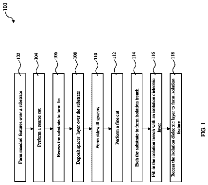
Method of making a FinFET device
A method of fabricating a fin-like field-effect transistor (FinFET) device is disclosed.
US 9,929,199 B2 · Assignee: SONY SEMICONDUCTOR SOLUTIONS CORPORATION · Inventors: Igarashi; Takahiro et al.
Sheet 1 of 34 from the published document. All sheets in the USPTO PDF
There is provided a radiation detector including: a plurality of photoelectric conversion devices, each photoelectric conversion device formed at least partially within an embedding layer and having a light receiving surface situated at least partially outside of the embedding layer, and a plurality of scintillator crystals, at least a first scintillator crystal of the plurality of scintillator crystals in contact with at least one light receiving surface at a proximal end, wherein a cross-section of the first scintillator crystal at the proximal end is smaller than a cross-section of the first scintillator crystal at a distal end.
Various imaging units have been proposed as an imaging unit that includes a photoelectric conversion device built in each pixel (imaging pixel). For example, PTL 1 refers to a radiation imaging unit as an example of such an imaging unit that includes a photoelectric conversion device. CITATION LIST Patent Literature
1 of 34 drawing sheets so far from the published document, cropped to the drawing. Every sheet is in the USPTO PDF.
What the patent claimed, word for word. All of it is now free to use.
This application claims priority to Japanese Priority Patent Application JP 2013-177175 filed Aug. 28, 2013, the entire contents of which are hereby incorporated by reference.
The present technology relates to a radiation detector that detects radiation such as alpha rays, beta rays, gamma rays, and X-rays, and to a method of manufacturing the radiation detector. Also, the present technology relates to an imaging unit and an imaging and display system that include the radiation detector.
Various imaging units have been proposed as an imaging unit that includes a photoelectric conversion device built in each pixel (imaging pixel). For example, PTL 1 refers to a radiation imaging unit as an example of such an imaging unit that includes a photoelectric conversion device. CITATION LIST Patent Literature
JP 2011-135561A SUMMARY Technical Problem
Generally, in an imaging unit as that described above, an image is obtained by driving a plurality of pixels. There has been proposed various techniques to achieve higher image quality for thus-obtained image. However, it is desired to propose an imaging unit that is capable of achieving further higher image quality.
It is desirable to provide a radiation detector capable of achieving higher image quality, and a method of manufacturing such a radiation detector. It is also desirable to provide an imaging unit and an imaging and display system that include such a radiation detector. Solution to Problem
According to an embodiment of the present technology, there is provided a radiation detector including: a plurality of photoelectric conversion regions each configured to convert light incident on a light receiving surface into a current signal; a discontinuous surface formed around the light receiving surface, the discontinuous surface being discontinuous with respect to the light receiving surface; and a scintillator layer formed with use of the light receiving surface as a crystal growth surface and configured to convert incident radiation into light.
According to an embodiment of the present technology, there is provided an imaging unit including: a radiation detector; and a drive section configured to drive the radiation detector. The radiation detector includes: a plurality of photoelectric conversion regions each configured to convert light incident on a light receiving surface into a current signal; a discontinuous surface formed around the light receiving surface, the discontinuous surface being discontinuous with respect to the light receiving surface,
a plurality of conversion circuits provided in correspondence with the plurality of photoelectric conversion regions in a one-to-one relationship and each configured to convert the current signal into a voltage signal; and a scintillator layer formed with use of the light receiving surface as a crystal growth surface and configured to convert incident radiation into light.
According to an embodiment of the present technology, there is provided an imaging and display system including: an imaging unit; and a display unit configured to perform image display based on an imaging signal obtained by the imaging unit. The imaging unit includes a radiation detector, and a drive section configured to drive the radiation detector. The radiation detector includes: a plurality of photoelectric conversion regions each configured to convert light incident on a light receiving surface into a current signal; a discontinuous surface formed around the light receiving surface, the discontinuous surface being discontinuous with respect to the light receiving surface, a plurality of conversion circuits provided in correspondence with the plurality of photoelectric conversion regions in a one-to-one relationship and each configured to convert the current signal into a voltage signal; and a scintillator layer formed with use of the light receiving surface as a crystal growth surface and configured to convert incident radiation into light.
In the radiation detector, the imaging unit, and the imaging and display system according to the embodiments of the present technology, the light receiving surface of each of the photoelectric conversion regions is surrounded by the discontinuous surface, and serves as the crystal growth surface of the scintillator layer. Accordingly, the light receiving surface is in direct contact with the scintillator layer. Therefore, it is possible to achieve light reception efficiency that is higher than, for example, light reception efficiency in a case where a member only used for allowing the scintillator layer to grow thereon is provided between the light receiving surface and the scintillator layer. Moreover, the light receiving surface is surrounded by the discontinuous surface. Therefore, when the scintillator layer is formed on the light receiving surface, the crystal interface extending in the thickness direction of the scintillator layer is formed in a region opposing the discontinuous surface due to discontinuity between the light receiving surface and the discontinuous surface. Accordingly, part of light generated in the scintillator layer is reflected by the crystal interface and enters the light receiving surface. Therefore, high resolution is achieved.
According to an embodiment of the present technology, there is provided a method of manufacturing a radiation detector, the method including: (A) transferring, to a substrate, part or all of a plurality of devices included in a device substrate, the plurality of devices being fixed onto a support substrate included in the device substrate, and the plurality of devices each being configured to convert light incident on a light receiving surface into a current signal; and (B) forming a scintillator layer with use of the light receiving surface as a crystal growth surface, the scintillator layer being configured to convert incident radiation into light.
In the method of manufacturing the radiation detector according to the embodiment of the present technology, part or all of the plurality of devices fixed to the device substrate are transferred to the substrate. Also, the light receiving surface of each of the devices transferred to the substrate serves as the crystal growth surface of the scintillator layer. Accordingly, the light receiving surface is in direct contact with the scintillator layer. Therefore, it is possible to achieve light reception efficiency that is higher than, for example, light reception efficiency in a case where a member only used for allowing the scintillator layer to grow thereon is provided between the light receiving surface and the scintillator layer. Moreover, the light receiving surface of each of the devices transferred to the substrate is surrounded by the spacing formed between the devices. Therefore, when the scintillator layer is formed on the light receiving surface, the crystal interface extending in the thickness direction of the scintillator layer is formed in a region opposing the spacing formed between the devices, due to discontinuity between the light receiving surface and the spacing formed between the devices. Accordingly, part of light generated in the scintillator layer is reflected by the crystal interface and enters the light receiving surface. Therefore, high resolution is achieved.
According to an embodiment of the present technology, there is provided a radiation detector, comprising a plurality of photoelectric conversion devices, each photoelectric conversion device formed at least partially within an embedding layer and having a light receiving surface situated at least partially outside of the embedding layer, and a plurality of scintillator crystals, at least a first scintillator crystal of the plurality of scintillator crystals in contact with at least one light receiving surface at a proximal end, wherein a cross-section of the first scintillator crystal at the proximal end is smaller than a cross-section of the first scintillator crystal at a distal end.
According to an embodiment of the present technology, there is provided a method of forming a radiation detector, comprising forming a plurality of photoelectric conversion devices on a substrate, at least a first photoelectric conversion device of the plurality of photoelectric conversion devices including one or more electrodes, wherein the first photoelectric conversion device is formed such that at least one of the one or more electrodes are coupled to a circuit formed within the substrate, forming an embedding layer on the substrate such that at least a portion of the first photoelectric conversion device is embedded within the embedding layer, and forming a scintillator layer on a surface of the first photoelectric conversion layer.
According to an embodiment of the present technology, there is provided an imaging unit, comprising a radiation detector, and a drive circuit configured to drive the radiation detector,
the radiation detector including a plurality of pixels, at least a first pixel of the plurality of pixels comprising a photoelectric conversion device formed at least partially within an embedding layer and having a light receiving surface situated at least partially outside of the embedding layer, and a first scintillator crystal in contact with the light receiving surface at a proximal end, wherein a cross-section of the first scintillator crystal at the proximal and is smaller than a cross-section of the first scintillator crystal at a distal end.
According to an embodiment of the present technology, there is provided an imaging and display system comprising an imaging unit, and a display unit configured to perform image display based on an imaging signal obtained by the imaging unit, the imaging unit including a radiation detector, and a drive circuit configured to drive the radiation detector, the radiation detector including a plurality of pixels, at least a first pixel of the plurality of pixels comprising a photoelectric conversion device formed at least partially within an embedding layer and having a light receiving surface situated at least partially outside of the embedding layer, and a first scintillator crystal in contact with the light receiving surface at a proximal end, wherein a cross-section of the first scintillator crystal at the proximal end is smaller than a cross-section of the first scintillator crystal at a distal end. Advantageous Effects of Invention
According to the radiation detector, the imaging unit, and the imaging and display system of the embodiments of the present technology, the light receiving surface is in direct contact with the scintillator layer, and the light receiving surface is surrounded by the discontinuous surface. Therefore, high light reception efficiency and high resolution are achieved. Accordingly, it is possible to achieve higher image quality in an image. It is to be noted that the advantageous effect of the present technology is not necessarily limited to the effects described above, and may be any of effects described in the present description.
According to the method of manufacturing the radiation detector of the embodiment of the present technology, the light receiving surface is in direct contact with the scintillator layer, and the light receiving surface is surrounded by the spacing formed between the devices. Therefore, high light reception efficiency and high resolution are achieved. Accordingly, it is possible to achieve higher image quality in an image. It is to be noted that the advantageous effect of the present technology is not necessarily limited to the effects described above, and may be any of the effects described in the present description.
It is to be understood that both the foregoing general description and the following detailed description are exemplary, and are intended to provide further explanation of the technology as claimed.
The accompanying drawings are included to provide a further understanding of the disclosure, and are incorporated in and constitute a part of this specification. The drawings illustrate embodiments and, together with the specification, serve to explain the principles of the technology.
FIG. 1 is a diagram illustrating an example of a cross-sectional configuration of a radiation detector according to a first embodiment of the present technology.
FIG. 2 is a diagram illustrating an example of a circuit configuration in the radiation detector shown in FIG. 1 .
FIG. 3 is a diagram illustrating an example of a cross-sectional configuration of a device shown in FIG. 1 .
FIG. 4 is a diagram illustrating another example of the cross-sectional configuration of the device shown in FIG. 1 .
FIG. 5 is a cross-sectional view for explaining an example of a process of manufacturing the radiation detector shown in FIG. 1 .
FIG. 6 is a cross-sectional view for explaining a step following a step shown in FIG. 5 .
FIG. 7 is a cross-sectional view for explaining a step following the step shown in FIG. 6 .
FIG. 8 is a cross-sectional view for explaining a step following the step shown in FIG. 7 .
FIG. 9 is a cross-sectional view for explaining a step following the step shown in FIG. 8 .
FIG. 10 is a cross-sectional view for explaining a step following the step shown in FIG. 9 .
FIG. 11 is a cross-sectional view for explaining a step following the step shown in FIG. 10 .
FIG. 12 is a cross-sectional view for explaining a step following the step shown in FIG. 11 .
FIG. 13 is a cross-sectional view illustrating a modification of the radiation detector shown in FIG. 1 .
FIG. 14 is a diagram illustrating an example of a circuit configuration of a wiring substrate and a circuit substrate shown in FIG. 13 .
FIG. 15 is a cross-sectional view illustrating a modification of the device shown in FIG. 3 .
FIG. 16 is a cross-sectional view illustrating a modification of the device shown in FIG. 4 .
FIG. 17 is a diagram illustrating an example of a cross-sectional configuration of a radiation detector according to a second embodiment of the present technology.
FIG. 18 is a diagram illustrating an example of a cross-sectional configuration of a device shown in FIG. 17 .
FIG. 19 is a cross-sectional view for explaining an example of a process of manufacturing the radiation detector shown in FIG. 17 .
FIG. 20 is a cross-sectional view for explaining a step following a step shown in FIG. 19 .
FIG. 21 is a cross-sectional view for explaining a step following the step shown in FIG. 20 .
FIG. 22 is a cross-sectional view for explaining a step following the step shown in FIG. 21 .
FIG. 23 is a cross-sectional view for explaining a step following the step shown in FIG. 22 .
FIG. 24 is a cross-sectional view for explaining a step following the step shown in FIG. 23 .
FIG. 25 is a cross-sectional view for explaining a step following the step shown in FIG. 24 .
FIG. 26 is a cross-sectional view for explaining a step following the step shown in FIG. 25 .
FIG. 27 is a cross-sectional view illustrating a modification of the radiation detector that includes the device shown in FIG. 3 .
FIG. 28 is a cross-sectional view illustrating a modification of the radiation detector that includes the device shown in FIG. 4 .
FIG. 29 is a cross-sectional view illustrating a modification of the radiation detector shown in FIG. 17 .
FIG. 30 is a cross-sectional view illustrating a modification of the radiation detector shown in FIG. 1 .
FIG. 31 is a cross-sectional view illustrating a modification of the radiation detector shown in FIG. 17 .
FIG. 32A is a cross-sectional view illustrating a modification of the radiation detector shown in FIG. 1 .
FIG. 32B is a cross-sectional view illustrating a modification of the radiation detector shown in FIG. 1 .
FIG. 32C is a cross-sectional view illustrating a modification of the radiation detector shown in FIG. 1 .
FIG. 33 is a cross-sectional view illustrating a modification of the radiation detector shown in FIG. 17 .
FIG. 34 is a cross-sectional view illustrating a modification of the radiation detector shown in FIG. 1 .
FIG. 35 is a cross-sectional view illustrating a modification of the radiation detector shown in FIG. 17 .
FIG. 36 is a diagram illustrating an example of a cross-sectional configuration of a radiation detector according to a third embodiment of the present technology.
FIG. 37 is a cross-sectional view illustrating a modification of the radiation detector shown in FIG. 1 .
FIG. 38 is a cross-sectional view illustrating a modification of the radiation detector shown in FIG. 17 .
FIG. 39 is a cross-sectional view illustrating a modification of the radiation detector shown in FIG. 36 .
FIG. 40 is a diagram illustrating an example of a schematic configuration of an imaging unit according to a fourth embodiment of the present technology.
FIG. 41 is a diagram illustrating an example of a schematic configuration of a pixel circuit shown in FIG. 40 .
FIG. 42 is a diagram illustrating an example of a schematic configuration of an imaging and display system according to a fifth embodiment of the present technology.
FIG. 43 is a diagram illustrating an example of a schematic configuration of an imaging system according to a sixth embodiment of the present technology.
Some embodiments of the present technology will be described below in detail referring to the drawings. The description will be provided in the following order. 1. First Embodiment (Radiation Detector) An example in which a photoelectric conversion region is provided in a chip-like device 2. Second Embodiment (Radiation Detector) An example in which a photoelectric conversion device and a conversion circuit are provided in a chip-like device 3. Modifications of First and Second Embodiments (Radiation Detector) An example in which a protective film covering the chip-like device is provided An example in which a protective film covering a scintillator layer is provided An example in which a plurality of photoelectric conversion regions are provided in a common substrate An example in which a plurality of photoelectric conversion regions and a plurality of conversion circuits are provided in a common substrate An example in which a light blocking layer is provided in a region, of a top surface of a substrate, other than a region of a light receiving surface 4. Third Embodiment (Radiation Detector) An example in which a plurality of radiation detectors are arranged in a matrix 5. Modification (Radiation Detector) An example in which the scintillator layer is omitted 6. Fourth Embodiment (Imaging Unit) 7. Fifth Embodiment (Imaging and Display System) 8. Sixth Embodiment (Imaging System) (1. First Embodiment) (Configuration)
First, description will be provided of a radiation detector 1 according to a first embodiment of the present technology. FIG. 1 illustrates an example of a cross-sectional configuration of the radiation detector 1 according to the present embodiment. The radiation detector 1 detects radiation such as alpha rays, beta rays, gamma rays, and X-rays. The radiation detector 1 uses an indirect conversion method. The indirect conversion method refers to a method in which radiation is converted into an optical signal, and then, the optical signal is converted into an electric signal. The radiation detector 1 may include, for example, a circuit substrate 10 , a plurality of devices 20 , a scintillator layer 30 , and a reflection plate 40 .
FIG. 2 illustrates an example of a circuit configuration of a part, in the radiation detector 1 , that converts an optical signal into an electric signal. The circuit substrate 10 includes a plurality of pixel circuits 13 and various wirings for connecting the respective pixel circuits 13 and the respective devices 20 to an external circuit. The pixel circuits 13 are provided in correspondence with the devices 20 in a one-to-one relationship. The pixel circuit 13 includes a drive circuit that drives the device 20 . In each of the pixel circuits 13 , the drive circuit may include, for example, a switch device 13 S (see FIG. 2 ) that is connected in series to the device 20 . In other words, the switch devices 13 S are allocated for the pixel circuits 13 in a one-to-one relationship. The switch device 13 S controls ON and OFF of the device 20 based on a control signal supplied from outside. The switch device 13 S may include, for example, a TFT. As shown in FIG. 2 , the circuit substrate 10 may include, for example, a plurality of data lines 12 A, a plurality of gate lines 12 B, and a plurality of bias lines 12 C, as various wirings. For example, each of the data lines 12 A may be connected to an output terminal of each of the pixel circuits 13 (for example, the switch devices 13 S) arranged side by side in a column direction, and may be a wiring that extracts a signal outputted from the pixel circuit 13 to the outside. Each of the gate lines 12 B may be connected to a gate terminal of each of the pixel circuits 13 (for example, the switch devices 13 S) arranged side by side in a row direction, and may be a wiring that supplies the pixel circuit 13 with a signal for driving the pixel circuit 13 . Each of the bias lines 12 C may be connected to an end of each of the devices 20 arranged side by side in the column direction, and may be a wiring that supplies a bias voltage to the device 20 .
The pixel circuit 13 may further include, for example, a conversion circuit, an amplifier circuit, and an A-D conversion circuit. The conversion circuit converts a current signal outputted from the device 20 into a voltage signal. The amplifier circuit amplifies the voltage signal outputted from the conversion circuit. The A-D conversion circuit converts an analog signal outputted from the amplifier circuit into a digital signal. It is to be noted that the circuit substrate 10 may include a plurality of such conversion circuits, a plurality of such amplifier circuits, and a plurality of such A-D conversion circuits in a circuit different from the pixel circuit 13 . When the circuit substrate 10 includes the plurality of conversion circuits in a circuit different from the pixel circuit 13 , each of the conversion circuits may be provided for a plurality of devices 20 . In this case, the plurality of devices 20 allocated to each conversion circuit may be formed as a single device. When the circuit substrate 10 includes the plurality of amplifier circuits in a circuit different from the pixel circuit 13 , each amplifier circuit may be provided for a plurality of devices 20 . When the circuit substrate 10 includes the plurality of A-D conversion circuits in a circuit different from the pixel circuit 13 , each of the A-D conversion circuits may be provided for a plurality of devices 20 .
The circuit substrate 10 may be configured, for example, of a support substrate 11 , and a circuit layer 12 and an embedding layer 15 that are laminated in order on the support substrate 11 . The support substrate 11 may be configured, for example, of an insulating substrate such as a glass substrate. The support substrate 11 may be a substrate (a light blocking layer) that has light non-transmission characteristics such as a silicon substrate. The embedding layer 15 is provided for preventing a material such as solder that is used for a later-described bump 23 from giving influence to the scintillator layer 30 . At least the bumps 23 are embedded in the embedding layer 15 . The embedding layer 15 may be configured, for example, of a material such as underfill resin. Examples of the underfill resin may include parylene resin, acryl-based resin, epoxy-based resin, silicone resin, and urethane-based resin. The embedding layer 15 may be a light blocking layer that includes a material having light non-transmission characteristics.
The circuit layer 12 may include, for example, the plurality of pixel circuits 13 and a plurality of pad electrodes 14 . The circuit layer 12 may further include, for example, wirings that connect the respective pixel circuits 13 and the respective devices 20 to an external circuit. As shown in FIG. 2 , the circuit layer 12 may include, for example, the plurality of data lines 12 A, the plurality of gate lines 12 B, and the plurality of bias lines 12 C. The pad electrode 14 is a terminal electrode that is electrically connected to the pixel circuit 13 . The pad electrode 14 is exposed to a top surface of the circuit layer 12 . The pad electrode 14 is in contact with the bump 23 (which will be described later) in the device 20 . One pixel circuit 13 and a plurality of pad electrodes 14 are allocated for each device 20 , and may be arranged, for example, in each region that opposes the device 20 . Each pad electrode 14 may include, for example, an electrically-conductive metal material such as UBM (Under Bump Metallization). The UBM may be configured, for example, of nickel (Ni), and serves as a solder diffusion suppressing layer. In the circuit layer 12 , the pixel circuits 13 may be embedded, for example, in an interlayer insulating film. The interlayer insulating film may be configured, for example, of a material such as silicon oxide (SiO2) and silicon oxynitride (SiON). The interlayer insulating film may serve as a light blocking layer that includes a material having light non-transmission characteristics.
The plurality of devices 20 are mounted on the common circuit substrate 10 . The plurality of devices 20 may be arranged, for example, two-dimensionally on the circuit substrate 10 . Each of the devices 20 may have been transferred from a device substrate 100 onto a circuit substrate 10 A by a transfer technique as will be described later, for example. The devices 20 are arranged to be away from one another in a plane. Therefore, a top surface (i.e., a light receiving surface 20 A) of each of the devices 20 is surrounded by a spacing that is formed between the two adjacent devices 20 . A width of the spacing may be, for example, equivalent to or smaller than a lateral width of the device 20 . A bottom surface of the spacing configures a top surface of the circuit substrate 10 (for example, a top surface of the embedding layer 15 ), and configures a discontinuous surface 15 A that is discontinuous with respect to the light receiving surface 20 A. Herein, the wording “discontinuous with respect to the light receiving surface 20 A” does not only refer to a state that the light receiving surface 20 A and the discontinuous surface 15 A are not arranged in the same plane. The wording “discontinuous with respect to the light receiving surface 20 A” also refers to discontinuity that achieves formation of a crystal interface 31 A (which will be described later) that extends in a thickness direction of the scintillator layer 30 when the scintillator layer 30 is formed in a manufacturing process of the radiation detector.
Each device 20 may be, for example, a chip of a sub-millimeter size. It is to be noted that each device 20 may have a size larger than a sub-millimeter size. Each device 20 is a separated part that serves as a component, for example, of a unit, an electronic circuit, etc. Each device 20 is a chip-like part. Each device 20 may include, for example, a chip-like function section 21 , a plurality of electrodes 22 , and the bump 23 . The function section 21 has a function of converting light incident on a top surface of the function section 21 into a current signal. The top surface of the function section 21 serves as the light receiving surface 20 A of the device 20 . The light receiving surface 20 A may be, for example, a planarized surface. It is to be noted that the light receiving surface 20 A may be a curved surface that has concavities and convexities. Each electrode 22 is a terminal electrode that is electrically connected to a photoelectric conversion device 120 (which will be described later) in the function section 21 . Each electrode 22 is arranged on a bottom surface (i.e., a surface opposite from the light receiving surface 20 A) of the function section 21 . Each electrode 22 is in contact with the bump 23 . Each electrode 22 may include, for example, an electrically-conductive metal material such as UBM. The bump 23 is in contact with the electrode 22 and the pad electrode 14 . The bump 23 may be configured, for example, of alloy that includes lead or tin as a main component. The bump 23 may be formed, for example, by electrolytic plating, imprinting of solder paste, etc.
FIGS. 3 and 4 each illustrate an example of a cross-sectional configuration of the device 20 . FIG. 3 illustrates an example of the cross-sectional configuration of the device 20 that includes the photoelectric conversion device 120 that is configured to detect light entering from the top surface of the photoelectric conversion device 120 . In other words, the photoelectric conversion device 120 shown in FIG. 3 has a top-surface illumination structure. FIG. 4 illustrates an example of the cross-sectional configuration of the device 20 that includes the photoelectric conversion device 120 that is configured to detect light entering from a back surface of the photoelectric conversion device 120 .
In other words, the photoelectric conversion device 120 shown in FIG. 4 has a back-surface illumination structure.
(Top-Surface Illumination Structure, FIG. 3 )
As shown in FIG. 3 , the device 20 may have, for example, a structure in which an insulating layer 111 , an insulating layer 112 , and an insulating layer 113 are laminated in order from the light receiving surface 20 A. A back surface (i.e., a surface opposite from a surface on which the insulating layers 112 and 113 are laminated) of the insulating layer 111 serves as the light receiving surface 20 A. The insulating layer 111 may be configured, for example, of silicone-based resin. The insulating layers 112 and 113 may each be configured, for example, also of a material such as silicone-based resin.
As shown in FIG. 3 , the device 20 may further include, for example, the photoelectric conversion device 120 and an electrically-conductive path that electrically connects the photoelectric conversion device 120 to the electrode 22 . The electrically-conductive path may be configured, for example, of a pad electrode 114 , a wiring layer 115 , a connection section 116 , and a connection section 117 that are arranged in order from the photoelectric conversion device 120 . The photoelectric conversion device 120 may be arranged, for example, in the insulating layer 113 . The pad electrode 114 , the wiring layer 115 , and the connection section 116 may be arranged, for example, in the insulating layer 112 . The connection section 117 may be arranged, for example, in the insulating layer 113 .
The photoelectric conversion device 120 may have, for example, a structure in which a semiconductor layer including a photoelectric conversion region 122 , a plurality of electrodes 123 , and a plurality of bumps 124 are laminated on a substrate 121 . Accordingly, one photoelectric conversion region 122 is formed in each device 20 . The device 20 includes a semiconductor layer that includes the photoelectric conversion region 122 and the insulating layer 111 that is arranged above this semiconductor layer. In the photoelectric conversion device 120 , the semiconductor layer including the photoelectric conversion region 122 is arranged in a position closer to the light receiving surface 20 A, and the substrate 121 is arranged in a position closer to the bottom surface of the device 20 . Each electrode 123 is electrically connected to the photoelectric conversion region 122 . Each bump 124 is arranged in contact with the electrode 123 and with the pad electrode 114 . The pad electrode 114 and the connection section 116 are arranged in contact with the wiring layer 115 . The connection section 117 is arranged in contact with the connection section 116 and with the electrode 22 .
The substrate 121 is configured of a semiconductor substrate. The photoelectric conversion region 122 is formed in the semiconductor layer that is formed on the substrate 121 . The photoelectric conversion region 122 may be configured, for example, of a p-type semiconductor layer, an i-type semiconductor layer, and an n-type semiconductor layer that are laminated in order. The photoelectric conversion region 122 (the semiconductor layer including the photoelectric conversion region 122 ) may be configured, for example, of crystalline silicon or amorphous silicon. The electrode 123 , the bump 124 , the pad electrode 114 , the wiring layer 115 , the connection section 116 , and the connection section 117 are each configured of an electrically-conductive metal material.
(Back-Surface Illumination Structure, FIG. 4 )
As shown in FIG. 4 , the device 20 may have, for example, a structure in which a semiconductor layer including the photoelectric conversion region 122 , the plurality of electrodes 22 , and the plurality of bumps 23 are laminated on the substrate 121 . In the device 20 , the semiconductor layer including the photoelectric conversion region 122 is arranged in a position closer to the light receiving surface 20 A, and the substrate 121 is arranged in a position closer to the bottom surface of the device 20 . A back surface (a surface opposite from a surface on which the semiconductor layer including the photoelectric conversion region 122 is laminated) of the substrate 121 serves as the light receiving surface 20 A.
The scintillator layer 30 converts a wavelength of radiation incident on the light receiving surface 20 A into a wavelength in a range of sensitivity of the photoelectric conversion region 122 . Specifically, the scintillator layer 30 converts the radiation incident on the light receiving surface 20 A into light. The scintillator layer 30 may be configured, for example, of a fluorescent material that converts radiation such as alpha rays, beta rays, gamma rays, and X-rays into visible light. Examples of such a fluorescent material may include a material obtained by adding thallium (Tl) or sodium (Na) to cesium iodide (CsI) and a material obtained by adding thallium (Tl) to sodium iodide (NaI). Examples of the above-mentioned fluorescent material may include a material obtained by adding europium (Eu) to cesium bromide (CsBr) and a material obtained by adding europium (Eu) to cesium fluorobromide (CsBrF).
The scintillator layer 30 is formed with the use of the light receiving surface 20 A as a crystal growth surface. The scintillator layer 30 may be formed, for example, by film formation by a vacuum deposition method. The scintillator layer 30 has the crystal interface 31 A that extends in the thickness direction of the scintillator layer 30 , in a region opposing the discontinuous surface 15 . The crystal interface 31 A extends from an end of the light receiving surface 20 A in the thickness direction of the scintillator layer 30 , and thereby, sections the scintillator layer 30 in correspondence with each of the devices 20 (or each of the photoelectric conversion regions 122 ). Therefore, the scintillator layer 30 includes a plurality of scintillator sections 31 that are each allocated to each of the devices 20 (or each of the photoelectric conversion regions 122 ) by the crystal interface 31 A.
The cross-sectional area of the scintillator section 31 in a position closer to the reflection plate 40 is larger than a cross-sectional area of the scintillator section 31 in a position closer to the light receiving surface 20 A. It is to be noted that the above-mentioned cross-sectional area refers to the area of a cross-section, of the scintillator section 31 , that is parallel to the light receiving surface 20 A. Therefore, a width d of a spacing between the two adjacent scintillator sections 31 is decreased from the discontinuous surface 15 A side to the reflection plate 40 side (the upper side of the scintillator section 31 ). As shown in FIG. 1 , the crystal interface 31 A may be, for example, a concave-like curved surface when viewed from the discontinuous surface 15 A side. An angle theta 1 , at the end of the light receiving surface 20 A, that is formed by the crystal interface 31 A and the light receiving surface 20 A is an obtuse angle. An angle theta 2 formed by a tangent plane 30 S of the crystal interface 31 A and the light receiving surface 20 A is 90 degrees or larger. The angle theta 2 decreases as a tangent point of the tangent plane 30 S is farther from the light receiving surface 20 A side and is closer to the reflection plate 40 side (the upper side of the scintillator section 31 ). Therefore, part of light that is generated in the scintillator section 31 and travels toward the light receiving surface 20 A is reflected by the crystal interface 31 A and is allowed to enter the light receiving surface 20 A. In other words, the scintillator section 31 serves as a light condensing lens. An air spacing is formed between the adjacent crystal interfaces 31 A. It is to be noted that a scintillator section formed with the use of the discontinuous surface 15 A as a crystal growth surface may be provided between the adjacent crystal interfaces 31 A. In this case, a side surface of the scintillator section that is formed with the use of the discontinuous surface 15 A as the crystal growth surface configures a crystal interface, and is arranged to oppose the side surface of the device 20 and the crystal interface 31 A with a predetermined spacing in between.
The reflection plate 40 has a role of returning, toward the device 20 , the light that is emitted from the scintillator layer 30 in a direction opposite from the device 20 . The reflection plate 40 may be configured of a moisture non-transmission material that substantially does not transmit moisture. In such a case, it is possible to prevent moisture from entering into the scintillator layer 30 with the use of the reflection plate 40 . The reflection plate 40 may be configured, for example, of thin-plate glass. The reflection plate 40 may be omitted. A reflection structure provided on the scintillator layer 30 may be a configuration other than the reflection plate 40 described above, and may be configured, for example, of a deposited film made of Al.
(Manufacturing Method)
Next, description will be provided of an example of a method of manufacturing the radiation detector 1 . FIGS. 5 to 12 illustrate a process of manufacturing the radiation detector 1 in order of steps. First, the device substrate 100 and the circuit substrate 10 A are prepared ( FIGS. 5 and 6 ).
The description continues in the full USPTO document.
About 6,421 words. The USPTO PDF has it with every drawing.
Fees are due 3.5, 7.5 and 11.5 years after grant. This patent expired on March 27, 2026, so the fee marked "not paid" was the one that went unpaid.
RADIATION DETECTOR, METHOD OF MANUFACTURING RADIATION DETECTOR, IMAGING UNIT, AND IMAGING AND DISPLAY SYSTEM
Filed Aug 2014 · published Jun 2016Radiation detector, imaging unit, and imaging and display system
Filed Aug 2014 · granted Mar 2018Earlier publications, parents and continuations. None of them can still be enforced, or this patent would not be listed.
Prior art cited by the examiner or applicant. Useful when you check your own idea for novelty.
Everything on this page comes from the documents linked above.


