Background of the invention
The present invention relates generally to data processing and, in particular, to translation entry invalidation in a multithreaded data processing system.
A conventional multiprocessor (MP) computer system comprises multiple processing units (which can each include one or more processor cores and their various cache memories), input/output (I/O) devices, and data storage, which can include both system memory (which can be volatile or nonvolatile) and nonvolatile mass storage. In order to provide enough addresses for memory-mapped I/O operations and the data and instructions utilized by operating system and application software, MP computer systems typically reference an effective address space that includes a much larger number of effective addresses than the number of physical storage locations in the memory mapped I/O devices and system memory. Therefore, to perform memory-mapped I/O or to access system memory, a processor core within a computer system that utilizes effective addressing is required to translate an effective address into a real address assigned to a particular I/O device or a physical storage location within system memory.
In the POWER™ RISC architecture, the effective address space is partitioned into a number of uniformly-sized memory pages, where each page has a respective associated address descriptor called a page table entry (PTE). The PTE corresponding to a particular memory page contains the base effective address of the memory page as well as the associated base real address of the page frame, thereby enabling a processor core to translate any effective address within the memory page into a real address in system memory. The PTEs, which are created in system memory by the operating system and/or hypervisor software, are collected in a page frame table.
In order to expedite the translation of effective addresses to real addresses during the processing of memory-mapped I/O and memory access instructions (hereinafter, together referred to simply as “memory referent instructions”), a conventional processor core often employs, among other translation structures, a cache referred to as a translation lookaside buffer (TLB) to buffer recently accessed PTEs within the processor core. Of course, as data are moved into and out of physical storage locations in system memory (e.g., in response to the invocation of a new process or a context switch), the entries in the TLB must be updated to reflect the presence of the new data, and the TLB entries associated with data removed from system memory (e.g., paged out to nonvolatile mass storage) must be invalidated. In many conventional processors such as the POWER™ line of processors available from IBM Corporation, the invalidation of TLB entries is the responsibility of software and is accomplished through the execution of an explicit TLB invalidate entry instruction (e.g., TLBIE in the POWER™ instruction set architecture (ISA)).
In MP computer systems, the invalidation of a PTE cached in the TLB of one processor core is complicated by the fact that each other processor core has its own respective TLB, which may also cache a copy of the target PTE. In order to maintain a consistent view of system memory across all the processor cores, the invalidation of a PTE in one processor core requires the invalidation of the same PTE, if present, within the TLBs of all other processor cores. In many conventional MP computer systems, the invalidation of a PTE in all processor cores in the system is accomplished by the execution of a TLB invalidate entry instruction within an initiating processor core and the broadcast of a TLB invalidate entry request from the initiating processor core to each other processor core in the system. The TLB invalidate entry instruction (or instructions, if multiple PTEs are to be invalidated) may be followed in the instruction sequence of the initiating processor core by one or more synchronization instructions that guarantee that the TLB entry invalidation has been performed by all processor cores.
In conventional MP computer systems, the TLB invalidate entry instruction and associated synchronization instructions are strictly serialized, meaning that hardware thread of the initiating processor core that includes the TLB invalidate entry instruction must complete processing each instruction (e.g., by broadcasting the TLB invalidate entry request to other processor cores) before execution proceeds to the next instruction of the hardware thread. As a result of this serialization, at least the hardware thread of the initiating processor core that includes the TLB entry invalidation instruction incurs a large performance penalty, particularly if the hardware thread includes multiple TLB invalidate entry instructions.
In multithreaded processing units, it is often the case that at least some of the queues, buffers, and other storage facilities of the processing unit are shared by multiple hardware threads. The strict serialization of the TLBIE invalidate entry instruction and associated synchronization instructions can cause certain of the requests associated with the TLB invalidation sequence to stall in these shared facilities, for example, while awaiting confirmation of the processing of the requests by other processor cores. If not handled appropriately, such stalls can cause other hardware threads sharing the storage facilities to experience high latency and/or to deadlock.
In view of the foregoing, the present invention recognizes that it would be useful and desirable to provide an improved method for maintaining coherency of PTEs in a multithreaded computer system.
Brief summary
According to one embodiment of a multithreaded data processing system including a plurality of processor cores, storage-modifying requests of a plurality of concurrently executing hardware threads are received in a shared queue. The storage-modifying requests include a translation invalidation request of an initiating hardware thread. The translation invalidation request is removed from the shared queue and buffered in sidecar logic in one of a plurality of sidecars each associated with a respective one of the plurality of hardware threads. While the translation invalidation request is buffered in the sidecar, the sidecar logic broadcasts the translation invalidation request so that it is received and processed by the plurality of processor cores. In response to confirmation of completion of processing of the translation invalidation request by the initiating processor core, the sidecar logic removes the translation invalidation request from the sidecar. Completion of processing of the translation invalidation request at all of the plurality of processor cores is ensured by a broadcast synchronization request.
In one embodiment, the subsequent memory referent instruction are ordered with reference to the broadcast synchronization request by execution of an additional synchronization instruction (e.g., HWSYNC).
Brief description of the several views of the drawings
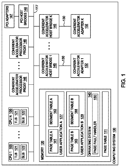
FIG. 1 is a high-level block diagram of an exemplary data processing system in accordance with one embodiment;
FIG. 2 is a more detailed block diagram of an exemplary processing unit in accordance with one embodiment;
FIG. 3 is a detailed block diagram of a processor core and lower level cache memory in accordance with one embodiment;
FIG. 4A is a first exemplary translation entry invalidation instruction sequence in accordance with one embodiment;
FIG. 4B is a second exemplary translation entry invalidation instruction sequence in accordance with one embodiment;
FIG. 5 is a high level logical flowchart of an exemplary method by which a processor core of a multiprocessor data processing system processes a translation entry invalidation instruction in accordance with one embodiment;
FIG. 6 is a high level logical flowchart of an exemplary method by which sidecar logic of a processing unit processes a translation entry invalidation request in accordance with one embodiment;
FIG. 7 is a high level logical flowchart of an exemplary method by which a snooper of a processing unit handles translation entry invalidation requests and translation synchronization requests in accordance with one embodiment;
FIG. 8 is a high level logical flowchart of an exemplary method by which an arbiter of a processing unit processes a translation entry invalidation request in accordance with one embodiment;
FIG. 9 is a high level logical flowchart of an exemplary method by which a translation sequencer of a processor core processes a translation entry invalidation request in accordance with one embodiment;
FIG. 10 is a high level logical flowchart of an exemplary method by which a store queue of a processing unit processes a translation invalidation complete request in accordance with one embodiment;
FIG. 11 is a high level logical flowchart of an exemplary method by which a processor core processes a translation synchronization instruction in accordance with one embodiment;
FIG. 12 is a high level logical flowchart of an exemplary method by which sidecar logic of a processing unit processes a translation synchronization request in accordance with one embodiment;
FIG. 13 is a high level logical flowchart of an exemplary method by which a processing core processes a page table synchronization instruction in accordance with one embodiment;
FIG. 14 is a high level logical flowchart of an exemplary method by which a processing unit processes a page table synchronization request in accordance with one embodiment;
FIG. 15 is a high level logical flowchart of an exemplary method by which snooper logic of a processing unit processes translation invalidation requests, translation invalidation complete requests, and page table synchronization requests in accordance with one embodiment; and
FIG. 16 is a data flow diagram illustrating a design process.
Detailed description
With reference now to the figures, wherein like reference numerals refer to like and corresponding parts throughout, and in particular with reference to FIG. 1 , there is illustrated a high level block diagram depicting an exemplary data processing system 100 in accordance with one embodiment. In the depicted embodiment, data processing system 100 is a cache coherent symmetric multiprocessor (SMP) data processing system including multiple processing nodes 102 for processing data and instructions. Processing nodes 102 are coupled to a system interconnect 110 for conveying address, data and control information. System interconnect 110 may be implemented, for example, as a bused interconnect, a switched interconnect or a hybrid interconnect.
In the depicted embodiment, each processing node 102 is realized as a multi-chip module (MCM) containing four processing units 104 a - 104 d , each preferably realized as a respective integrated circuit. The processing units 104 within each processing node 102 are coupled for communication to each other and system interconnect 110 by a local interconnect 114 , which, like system interconnect 110 , may be implemented, for example, with one or more buses and/or switches. System interconnect 110 and local interconnects 114 together form a system fabric.
As described below in greater detail with reference to FIG. 2 , processing units 104 each include a memory controller 106 coupled to local interconnect 114 to provide an interface to a respective system memory 108 . Data and instructions residing in system memories 108 can generally be accessed, cached and modified by a processor core in any processing unit 104 of any processing node 102 within data processing system 100 . System memories 108 thus form the lowest level of memory storage in the distributed shared memory system of data processing system 100 . In alternative embodiments, one or more memory controllers 106 (and system memories 108 ) can be coupled to system interconnect 110 rather than a local interconnect 114 .
Those skilled in the art will appreciate that SMP data processing system 100 of FIG. 1 can include many additional non-illustrated components, such as interconnect bridges, non-volatile storage, ports for connection to networks or attached devices, etc. Because such additional components are not necessary for an understanding of the described embodiments, they are not illustrated in FIG. 1 or discussed further herein. It should also be understood, however, that the enhancements described herein are applicable to data processing systems of diverse architectures and are in no way limited to the generalized data processing system architecture illustrated in FIG. 1 .
Referring now to FIG. 2 , there is depicted a more detailed block diagram of an exemplary processing unit 104 in accordance with one embodiment. In the depicted embodiment, each processing unit 104 is an integrated circuit including one or more processor cores 200 for processing instructions and data. In a preferred embodiment, each processor core 200 supports simultaneous multithreading (SMT) and thus is capable of independently executing multiple hardware threads of execution simultaneously.
The operation of each processor core 200 is supported by a multi-level memory hierarchy having at its lowest level a shared system memory 108 accessed via an integrated memory controller 106 . As illustrated, shared system memory 108 stores a page frame table 220 containing a plurality of page table entries (PTEs) 222 for performing effective-to-real address translation to enable access to the storage locations in system memory 108 . At its upper levels, the multi-level memory hierarchy includes one or more levels of cache memory, which in the illustrative embodiment include a store-through level one (L1) cache 302 (see FIG. 3 ) within and private to each processor core 200 , and a respective store-in level two (L2) cache 230 for each processor core 200 . Although the illustrated cache hierarchies includes only two levels of cache, those skilled in the art will appreciate that alternative embodiments may include additional levels (L3, L4, etc.) of on-chip or off-chip, private or shared, in-line or lookaside cache, which may be fully inclusive, partially inclusive, or non-inclusive of the contents the upper levels of cache.
Each processing unit 104 further includes an integrated and distributed fabric controller 216 responsible for controlling the flow of operations on the system fabric comprising local interconnect 114 and system interconnect 110 and for implementing the coherency communication required to implement the selected cache coherency protocol. Processing unit 104 further includes an integrated I/O (input/output) controller 214 supporting the attachment of one or more I/O devices (not depicted).
With reference now to FIG. 3 , there is illustrated a more detailed block diagram of an exemplary embodiment of a processor core 200 and its affiliated L2 cache 230 in accordance with one embodiment.
In the illustrated embodiment, processor core 200 includes one or more execution unit(s) 300 , which execute instructions from multiple simultaneous hardware threads of execution. The instructions can include, for example, arithmetic instructions, logical instructions, and memory referent instructions, as well as translation entry invalidation instructions (hereinafter referred to by the POWER™ ISA mnemonic TLBIE (Translation Lookaside Buffer Invalidate Entry)) and associated synchronization instructions. Execution unit(s) 300 can generally execute instructions of a hardware thread in any order as long as data dependencies and explicit orderings mandated by synchronization instructions are observed.
Processor core 200 additionally includes a memory management unit (MMU) 308 responsible for translating target effective addresses determined by the execution of memory referent instructions in execution unit(s) 300 into real addresses. MMU 308 performs effective-to-real address translation by reference to one or more translation structure(s) 310 , such as a translation lookaside buffer (TLB), block address table (BAT), segment lookaside buffers (SLBs), etc. The number and type of these translation structures varies between implementations and architectures. If present, the TLB reduces the latency associated with effective-to-real address translation by caching PTEs 222 retrieved from page frame table 220 . A translation sequencer 312 associated with translation structure(s) 310 handles invalidation of effective-to-real translation entries held within translation structure(s) 310 and manages such invalidations relative to memory referent instructions in flight in processor core 200 .
Processor core 200 additionally includes various storage facilities shared by the multiple hardware threads supported by processor core 200 . The storage facilities shared by the multiple hardware threads include an L1 store queue 304 that temporarily buffers store and synchronization requests generated by execution of corresponding store and synchronization instructions by execution unit(s) 300 . Because L1 cache 302 is a store-through cache, meaning that coherence is fully determined at a lower level of cache hierarchy (e.g., at L2 cache 230 ), requests flow through L1 STQ 304 and then pass via bus 318 to L2 cache 230 for processing. The storage facilities of processor core 200 shared by the multiple hardware threads additionally include a load miss queue (LMQ) 306 that temporarily buffers load requests that miss in L1 cache 302 . Because such load requests have not yet been satisfied, they are subject to hitting the wrong memory page if the address translation entry utilized to obtain the target real addresses of the load requests are invalidated before the load requests are satisfied. Consequently, if a PTE or other translation entry is to be invalidated, any load requests in LMQ 306 that depends on that translation entry has to be drained from LMQ 306 and be satisfied before the effective address translated by the relevant translation entry can be reassigned.
Still referring to FIG. 3 , L2 cache 230 includes a cache array 332 and a L2 directory 334 of the contents of cache array 332 . Assuming cache array 332 and L2 directory 334 are set associative as is conventional, storage locations in system memories 108 are mapped to particular congruence classes within cache array 332 utilizing predetermined index bits within the system memory (real) addresses. The particular memory blocks stored within the cache lines of cache array 332 are recorded in L2 directory 334 , which contains one directory entry for each cache line. While not expressly depicted in FIG. 3 , it will be understood by those skilled in the art that each directory entry in cache directory 334 includes various fields, for example, a tag field that identifies the real address of the memory block held in the corresponding cache line of cache array 332 , a state field that indicates the coherency state of the cache line, an LRU (Least Recently Used) field indicating a replacement order for the cache line with respect to other cache lines in the same congruence class, and inclusivity bits indicating whether the memory block is held in the associated L1 cache 302 .
L2 cache 230 additionally includes an L2 STQ 320 that receives storage-modifying requests and synchronization requests from L1 STQ 304 via interface 318 and buffers such requests. It should be noted that L2 STQ 320 is a unified store queue that buffers requests for all hardware threads of the affiliated processor core 200 . Consequently, all of the threads' store requests, TLBIE requests and associated synchronization requests flows through L2 STQ 320 . Although in most embodiments L2 STQ 320 includes multiple entries, L2 STQ 320 is required to function in a deadlock-free manner regardless of depth (i.e., even if implemented as a single entry queue). To this end, L2 STQ 320 is coupled by an interface 321 to associated sidecar logic 322 , which includes one request-buffering entry (referred to herein as a “sidecar”) 324 per hardware thread supported by the affiliated processor core 200 . As such, the number of sidecars 324 is unrelated to the number of entries in L2 STQ 320 . As described further herein, use of sidecars 324 allows potentially deadlocking requests to be removed from L2 STQ 320 so that no deadlocks occur during invalidation of a translation entry.
L2 cache 230 further includes dispatch/response logic 336 that receives local load and store requests initiated by the affiliated processor core 200 via buses 327 and 328 , respectively, and remote requests snooped on local interconnect 114 via bus 329 . Such requests, including local and remote load requests, store requests, TLBIE requests, and associated synchronization requests, are processed by dispatch/response logic 336 and then dispatched to the appropriate state machines for servicing.
In the illustrated embodiment, the state machines implemented within L2 cache 230 to service requests include multiple Read-Claim (RC) machines 342 , which independently and concurrently service load (LD) and store (ST) requests received from the affiliated processor core 200 . In order to service remote memory access requests originating from processor cores 200 other than the affiliated processor core 200 , L2 cache 230 also includes multiple snoop (SN) machines 344 . Each snoop machine 344 can independently and concurrently handle a remote memory access request snooped from local interconnect 114 . As will be appreciated, the servicing of memory access requests by RC machines 342 may require the replacement or invalidation of memory blocks within cache array 332 (and L1 cache 302 ). Accordingly, L2 cache 230 also includes CO (castout) machines 340 that manage the removal and writeback of memory blocks from cache array 332 .
In the depicted embodiment, L2 cache 230 additionally includes multiple translation snoop (TSN) machines 346 , which are utilized to service TLBIE requests and associated synchronization requests. It should be appreciated that in some embodiments, TSN machines 346 can be implemented in another sub-unit of a processing unit 104 , for example, a non-cacheable unit (NCU) (not illustrated) that handles non-cacheable memory access operations. In at least one embodiment, the same number of TSN machines 346 is implemented at each L2 cache 230 in order to simplify implementation of a consensus protocol (as discussed further herein) that coordinates processing of multiple concurrent TLBIE requests within data processing system 100 .
TSN machines 346 are all coupled to an arbiter 348 that selects requests being handled by TSN machines 346 for transmission to translation sequencer 312 in processor core 200 via bus 350 . In at least some embodiments, bus 350 is implemented as a unified bus that transmits not only requests of TSN machines 346 , but also returns data from the L2 cache 230 to processor core 200 , as well as other operations. It should be noted that translation sequencer 312 must accept requests from arbiter 348 in a non-blocking fashion in order to avoid deadlock.
Referring now to FIG. 4A , there is depicted a first exemplary translation entry invalidation instruction sequence 400 that may be executed by a processor core 200 of data processing system 100 in accordance with one embodiment. The purpose of instruction sequence 400 is to: (a) disable a translation entry (e.g., PTE 222 ) in page frame table 220 so that the translation entry does not get reloaded by any MMU 308 of data processing system 100 , (b) invalidate any copy of the translation entry (or other translation entry that translates the same effective address as the translation entry) cached by any processor core 200 in data processing system 100 , and (c) drain all the outstanding memory access requests that depend on the old translation entry before the effective address is re-assigned. If the translation were updated before the store requests that depend on the old translation entry drain, the store requests may corrupt the memory page identified by old translation entry. Similarly, if load requests that depend on the old translation entry and that miss L1 cache 302 were not satisfied before the translation is reassigned, the load requests would read data from a different memory page than intended and thus observe data not intended to be visible to the load requests.
Instruction sequence 400 , which may be preceded and followed by any arbitrary number of instructions, begins with one or more store (ST) instructions 402 . Each store instruction 402 , when executed, causes a store request to be generated that, when propagated to the relevant system memory 108 , marks a target PTE 222 in page frame table 220 as invalid. Once the store request has marked the PTE 222 as invalid in page frame table 220 , MMUs 308 will no longer load the invalidated translation from page frame table 220 .
Following the one or more store instructions 402 in instruction sequence 400 is a heavy weight synchronization (i.e., HWSYNC) instruction 404 , which is a barrier that ensures that the following TLBIE instruction 406 doesn't get reordered by processor core 200 such that it executes in advance of any of store instruction(s) 402 . Thus, HWSYNC instruction 404 ensures that if a processor core 200 reloads a PTE 222 from page frame table 220 after TLBIE instruction 406 invalidates cached copies of the PTE 222 , the processor core 200 is guaranteed to have observed the invalidation due to a store instruction 402 and therefore will not use or re-load the target PTE 222 into translation structure(s) 310 until the effective address translated by the target PTE 222 is re-assigned and set to valid.
Following HWSYNC instruction 404 in instruction sequence 400 is at least one TLBIE instruction 406 , which when executed generates a corresponding TLBIE request that invalidates any translation entries translating the target effective address of the TLBIE request in all translation structures 310 throughout data processing system 100 . The one or more TLBIE instructions 406 are followed in instruction sequence 400 by a translation synchronization (i.e., TSYNC) instruction 408 that ensures that, prior to execution of the thread proceeding to succeeding instructions, the TLBIE request generated by execution of TLBIE instruction 406 has finished invalidating all translations of the target effective address in all translation structures 310 throughout data processing system 100 and all prior memory access requests depending on the now-invalidated translation have drained.
Instruction sequence 400 ends with a second HWSYNC instruction 410 that enforces a barrier that prevents any memory referent instructions following HWSYNC instruction 410 in program order from executing until TSYNC instruction 406 has completed its processing. In this manner, any younger memory referent instruction requiring translation of the target effective address of the TLBIE request will receive a new translation rather than the old translation invalidated by TLBIE request. It should be noted that HWSYNC instruction 410 does not have any function directly pertaining to invalidation of the target PTE 222 in page frame table, the invalidation of translation entries in translation structures 310 , or draining of memory referent instructions that depend on the old translation.
To promote understanding of the inventions disclosed herein, the progression of a TLBIE instruction 406 and the TLBIE request generated therefrom are described from inception to completion with reference to FIGS. 5-10 . FIGS. 11 and 12 additionally depict the progression of TSYNC instruction 408 and its corresponding TSYNC request, which ensure that the invalidation requested by the TLBIE request has completed on all snooping processor cores 200 .
Referring first to FIG. 5 , there is illustrated a high level logical flowchart of an exemplary method by which an initiating processor core 200 of a multiprocessor data processing system 100 processes a translation entry invalidation (e.g., TLBIE) instruction in accordance with one embodiment. The illustrated process represents the processing performed in a single hardware thread, meaning that multiple of these processes can be performed concurrently (i.e., in parallel) on a single processor core 200 , and further, that multiple of these processes can be performed concurrently on various different processing cores 200 throughout data processing system 100 . As a result, multiple different address translation entries buffered in the various processor cores 200 of data processing system 100 can be invalidated by different initiating hardware threads in a concurrent manner.
The illustrated process begins at block 500 and then proceeds to block 501 , which illustrates execution of a TLBIE instruction 406 in an instruction sequence 400 by execution unit(s) 300 of a processor core 200 . Execution of TLBIE instruction 406 determines a target effective address for which all translation entries buffered in translation structure(s) 310 throughout data processing system 100 are to be invalidated. In response to execution of TLBIE instruction 406 , processor core 200 pauses the dispatch of any additional instructions in the initiating hardware thread because in the exemplary embodiment of FIG. 3 sidecar logic 322 includes only a single sidecar 324 per thread, meaning that at most one TLBIE request per thread can be active at a time. In other embodiments having multiple sidecars 324 per thread, multiple concurrently active TLBIE requests per thread can be supported.
At block 504 , a TLBIE request corresponding to TLBIE instruction 406 is generated and issued to L1 STQ 304 . The TLBIE request may include, for example, a transaction type indicating the type of the request (i.e., TLBIE), the effective address for which cached translations are to be invalidated, and an indication of the initiating processor core 200 and hardware thread that issued the TLBIE request. Processing of requests in L1 STQ 304 progresses, and the TLBIE request eventually moves from L1 STQ 304 to L2 STQ 320 via bus 318 as indicated at block 506 . The process then proceeds to block 508 , which illustrates that the initiating processor core 200 continues to refrain from dispatching instructions within the initiating hardware thread until it receives a TLBCMPLT_ACK signal from the storage subsystem via bus 325 , indicating that processing of the TLBIE request by the initiating processor core 200 is complete. (Generation of the TLBCMPLT_ACK signal is described below with reference to block 1010 of FIG. 10 .) It should also be noted that because dispatch of instructions within the initiating thread is paused, there can be no contention for the sidecar 324 of the initiating thread by a TSYNC request corresponding to TSYNC instruction 408 , as, for any given thread, only one of the two types of requests can be present in L2 STQ 320 and sidecar logic 322 at a time.
In response to a determination at block 508 that a TLBCMPLT_ACK signal has been received, the process proceeds from block 508 to block 510 , which illustrates processor core 200 resuming dispatch of instructions in the initiating thread; thus, release of the thread at block 510 allows processing of TSYNC instruction 408 (which is the next instruction in instruction sequence 400 ) to begin as described below with reference to FIG. 11 . Thereafter, the process of FIG. 5 ends at block 512 .
Referring now to FIG. 6 , there is depicted a high level logical flowchart of an exemplary method by which sidecar logic 322 of an L2 cache 230 processes a translation entry invalidation (e.g., TLBIE) request of a hardware thread of the affiliated processor core 200 in accordance with one embodiment. The process of FIG. 6 is performed on a per-thread basis.
The process of FIG. 6 begins at block 600 and then proceeds to block 602 , which illustrates sidecar logic 322 determining whether or not a TLBIE request of a hardware thread of the affiliated processor core 200 has been loaded into L2 STQ 320 . If not, the process iterates at block 602 . However, in response to a determination that a TLBIE of a hardware thread of the affiliated processor core 200 has been loaded into L2 STQ 320 , sidecar logic 322 removes the TLBIE request from L2 STQ 320 and moves the TLBIE request via interface 321 into the sidecar 324 corresponding to the initiating thread (block 604 ). Removal of the TLBIE request from L2 STQ 320 ensures that no deadlock occurs due to inability of L2 STQ 320 to receive incoming requests from the associated processor core 200 and enables such requests to flow through L2 STQ 320 .
At block 606 , sidecar 324 participates in a consensus protocol (which may be conventional) via interface 326 and local interconnect 114 to ensure that one (and only one) TSN machine 346 in each and every L2 cache 230 receives its TLBIE request. In addition, the consensus protocol ensures that the various TSN machines 346 only take action to service the TLBIE request once all of the corresponding TSN machines 346 have received the TLBIE request. Thereafter, the process returns to block 602 , which has been described.
With reference now to FIG. 7 , there is illustrated a high level logical flowchart of an exemplary method by which TSN machines 346 processes TLBIE requests and TSYNC requests in accordance with one embodiment. The illustrated process is independently and concurrently performed for each TSN machine 346 .
The process begins at block 700 and then proceeds to blocks 702 and 720 . Block 702 and succeeding block 704 illustrate that in response to receipt of a TLBIE request via the consensus protocol a TSN machine 346 buffers the TLBIE request and assumes a TLBIE_active state. The TLBIE request, which is broadcast over the system fabric 110 , 114 to the L2 cache 230 of the initiating processor core 200 and those of all other processor cores 200 of data processing system 100 at block 606 of FIG. 6 , is received by an L2 cache 230 via interface 329 , processed by dispatch/response logic 336 and then assigned to the TSN machine 346 . As noted above, in a preferred embodiment, the consensus protocol enforces the condition that the TLBIE request is allocated a TSN machine 346 in one L2 cache 230 only if a TSM machine 346 is similarly allocated to the TLBIE request by all other L2 caches 230 . The TSN machine 346 assuming the TLBIE_active state informs the associated arbiter 348 that a TLBIE request is ready to be processed, as described further below with reference to block 802 of FIG. 8 .
Block 706 illustrates TSN machine 346 remaining in the TLBIE_active state until processing of the TLBIE request by the associated processor core 200 (i.e., invalidation of the relevant translation entries in translation structure(s) 310 and draining of relevant memory referent requests from processor core 200 ) is completed, as indicated by receipt of a TLBCMPLT_ACK signal via signal line 330 . In response to receipt of the TLBCMPLT_ACK signal, the TLBIE_active state is reset, and the TSN machine 346 is released for reallocation (block 708 ). Thereafter, the process of FIG. 7 returns from block 708 to block 702 , which has been described.
Referring now to blocks 720 - 724 , a TSN machine 346 determines at block 720 if it is in the TLBIE_active state established at block 704 . If not, the process iterates at block 720 . If, however, the TSN machine 346 is in the TLBIE_active state established at block 704 , the TSN machine 346 monitors to determine if a TSYNC request for the initiating hardware thread of its TLBIE request has been detected (block 722 ). If no TSYNC request is detected, the process continues to iterate at blocks 720 - 722 . However, in response to a detection of a TSYNC request of the initiating hardware thread of its TLBIE request while TSN machine 346 is in the TLBIE_active state, TSN machine 346 provides a Retry coherence response via the system fabric 110 , 114 , as indicated at block 724 . As discussed below with reference to block 1208 of FIG. 12 , a Retry coherence response by any TSN snooper 346 handling the TLBIE request for the initiating hardware thread forces the TSYNC request to be reissued by the source L2 cache 230 and prevents the initiating hardware thread from progressing to HWSYNC instruction 410 until the TSYNC request completes without a Retry coherence response. The TSYNC request completes without a Retry coherence response when all processor cores 200 other than the initiating processor core 200 have completed their processing of the TLBIE request. (The TSYNC request is not issued by the initiating processor core 200 until it has completed processing the TLBIE request due to the dispatch of instructions being paused for processing of the TLBIE request, as discussed above with reference to block 508 of FIG. 5 .)
Referring now to FIG. 8 , there is a high level logical flowchart of an exemplary method by which an arbiter 348 of the L2 cache 230 processes a TLBIE request in accordance with one embodiment. The process begins at block 800 and then proceeds to block 802 , which illustrates arbiter 348 determining whether or not any of its TSN machines 346 is in the TLBIE_active state. If not, the process of FIG. 8 iterates at block 802 . However, in response to determining that one or more of its TSN machines 346 is in the TLBIE_active state, arbiter 348 selects one of the TSN machines 346 in the TLBIE_active state that has not been previously had its TLBIE request forwarded and transmits its TLBIE request via interface 350 to the translation sequencer 312 of the affiliated processor core 200 (block 804 ). To avoid deadlock, translation sequencer 312 is configured to accept TLBIE requests within a fixed time and not arbitrarily delay accepting a TLBIE request.
The process proceeds from block 804 to block 806 , which depicts arbiter 348 awaiting receipt of a TLBCMPLT_ACK message indicating that the affiliated processor core 200 has, in response to the TLBIE request, invalidated the relevant translation entry or entries in translation structure(s) 310 and drained the relevant memory referent requests that may have had their target addresses translated by the invalidated translation entries. Thus, at block 806 , arbiter 348 is awaiting a TLBCMPLT_ACK message like both the initiating thread (block 508 ) and a TSN machine 346 in each of the L2 caches 230 (block 706 ). In response to receipt of a TLBCMPLT_ACK message at block 806 , the process returns to block 802 , which has been described. It should be noted that by the time the process returns to block 802 , the previously selected TSN machine 346 will not still be in the TLBIE_active state for the already processed TLBIE request because the TLBIE_active state will have been reset as illustrated at blocks 706 - 708 before the process returns to block 802 .
The process of FIG. 8 (and blocks 802 and 806 in particular) ensures that only one TLBIE request is being processed by the processor core 200 at a time. The serial processing of TLBIE requests by the processor core 200 eliminates the need to tag TLBCMPLT_ACK messages to associate them with TLBIE requests and simplifies instruction marking mechanisms, as discussed below with reference to FIG. 9 . Those skilled in the art will recognize, however, that in other embodiments the processor core 200 can be configured to service multiple TLBIE requests concurrently with some additional complexity.
The description continues in the full USPTO document.
 Lapsed, fee not paid4 drawings