Lapsed, fee not paid2 drawings
Cameras, Displays & Optics · US 9,927,651 B2
Display device
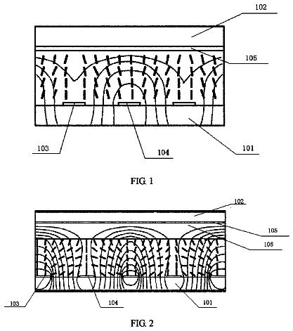
The present invention provides a display device, which includes a color filter, a quantum dot (QD)-injected photonic crystal film, and a backlight module.
US 9,927,658 B2 · Assignee: Sharp Kabushiki Kaisha · Inventors: Kawamura; Takehiko et al.
Sheet 1 of 12 from the published document. All sheets in the USPTO PDF
An active matrix substrate for a liquid crystal panel of an FFS mode includes a plurality of connecting units in a connecting region in order to electrically connect a common electrode, a first common main wiring 31 , and a second common main wiring 32 . The connecting unit includes a contact hole 41 that connects a connecting electrode 37 and the first common main wiring 31 , the connecting electrode 37 formed integrally with the common electrode, and a contact hole 42 that connects the connecting electrode 37 and the second common main wiring 32 . An amorphous Si film 122 of the second common main wiring 32 is formed larger than a main conductor part 131 of the second common main wiring 32 in a position of the contact hole 41 , and is covered with SiNx films 151, 152 that are protective insulating films. This prevents the connecting electrode from having a step disconnection at a pattern end of the common main wiring.
A liquid crystal display device has been widely used as a thin, light-weight, and low power consumption display device. A liquid crystal panel included in the liquid crystal display device has a structure formed by attaching an active matrix substrate and a counter substrate together, and providing a liquid crystal layer between the two substrates. A plurality of gate lines, a plurality of data lines, and a plurality of pixel circuits each including a thin film transistor (hereinafter referred to as TFT) and a pixel electrode are formed on the active matrix substrate. As a system for applying an electric field to the liquid crystal layer of the liquid crystal panel, a vertical electric field system and a lateral electric field system are known. In a liquid crystal panel of the vertical electric field system, an almost vertical electric field is applied to the liquid crystal layer by usin
1 of 12 drawing sheets so far from the published document, cropped to the drawing. Every sheet is in the USPTO PDF.
What the patent claimed, word for word. All of it is now free to use.
The present invention relates to a display device, and particularly relates to an active matrix substrate having a common electrode, a liquid crystal panel including the active matrix substrate, and a method for manufacturing the active matrix substrate having the common electrode.
A liquid crystal display device has been widely used as a thin, light-weight, and low power consumption display device. A liquid crystal panel included in the liquid crystal display device has a structure formed by attaching an active matrix substrate and a counter substrate together, and providing a liquid crystal layer between the two substrates. A plurality of gate lines, a plurality of data lines, and a plurality of pixel circuits each including a thin film transistor (hereinafter referred to as TFT) and a pixel electrode are formed on the active matrix substrate.
As a system for applying an electric field to the liquid crystal layer of the liquid crystal panel, a vertical electric field system and a lateral electric field system are known. In a liquid crystal panel of the vertical electric field system, an almost vertical electric field is applied to the liquid crystal layer by using the pixel electrode and a common electrode formed on the counter substrate. In a liquid crystal panel of the lateral electric field system, the common electrode is formed on the active matrix substrate together with the pixel electrode, and an almost lateral electric field is applied to the liquid crystal layer by using the pixel electrode and the common electrode. The liquid crystal panel of the lateral electric field system has an advantage of having a wider view angle than that in the liquid crystal panel of the vertical electric field system.
As the lateral electric field system, an IPS (In-Plane Switching) mode and an FFS (Fringe Field Switching) mode are known. In a liquid crystal panel of the IPS mode, the pixel electrode and the common electrode are each formed in the shape of comb teeth, and are disposed so as not to overlap each other in a plan view. In a liquid crystal panel of the FFS mode, a slit is formed either in the common electrode or the pixel electrode, and the pixel electrode and the common electrode are disposed so as to overlap each other via a protective insulating film in a plan view. The liquid crystal panel of the FFS mode has an advantage of having a higher aperture ratio than that in the liquid crystal panel of the IPS mode.
In the liquid crystal panel of the FFS mode, a common electrode signal to be applied to the common electrode is externally inputted. For applying the inputted common electrode signal to the common electrode, a common main wiring is formed in an outer peripheral portion (referred to as a picture-frame region) of a display region of the active matrix substrate. The common main wiring preferably has a portion (hereinafter referred to as a first common main wiring) formed in the same wiring layer as the gate line, and a portion (hereinafter referred to as a second common main wiring) formed in the same wiring layer as the data line. With the use of two kinds of common main wirings, by properly selecting the wiring layer of the common main wiring at an intersection of the gate line or the data line and the common main wiring, it is possible to reduce the number of times connecting the gate line and the number of times connecting the data line, and reduce the resistance of the gate line and the data line. Further, by selecting the wiring layer with small resistance and forming the common main wiring in the selected wiring layer, the resistance of the common main wiring can be reduced.
In the active matrix substrate having the two kinds of common main wirings, a connecting circuit is needed for electrically connecting the common main wirings formed in different wiring layers. For example, there is used a connecting circuit for electrically connecting the two kinds of common main wirings by using a connecting electrode formed integrally with the common electrode. Patent Document 1 describes an example of the connecting circuit for electrically connecting the common electrode and the two kinds of common main wirings in the liquid crystal panel of the FFS mode.
An active matrix substrate for the liquid crystal panel of the FFS mode is manufactured using five or six photomasks. Patent Document 2 describes a method for manufacturing the active matrix substrate using five photomasks. In the manufacturing method described in Patent Document 2, a semiconductor layer is patterned using a photomask for a source layer, without using a photomask for a semiconductor layer, and a channel region of a TFT is formed using a photomask for a pixel electrode layer. PRIOR ART DOCUMENT Patent Documents
[Patent Document 1] International Publication No.
WO 2013/77262
[Patent Document 2] Japanese Laid-Open Patent Publication No. 2010-191410 SUMMARY OF THE INVENTION Problems to be Solved by the Invention
However, when the connecting circuit for electrically connecting the common electrode and the two kinds of common main wirings is formed by using the manufacturing method described in Patent Document 2, the connecting electrode easily has a step disconnection at a pattern end of the second common main wiring (see FIG. 10 described later). When such a step disconnection occurs, rounding occurs in the common electrode signal, leading to the occurrence of display failure such as cross talk.
Accordingly, an object of the present invention is to provide an active matrix substrate that prevents a connecting electrode from having a step disconnection at a pattern end of a common main wiring, and to provide a liquid crystal panel including the active matrix substrate. Means for Solving the Problems
According to a first aspect of the present invention, there is provided an active matrix substrate, including: a plurality of gate lines formed in a first wiring layer; a plurality of data lines, each of which is a laminated wiring formed in a semiconductor layer, a second wiring layer, and a pixel electrode layer; a plurality of pixel circuits arranged corresponding to intersections of the gate lines and the data lines and each including a switching element and a pixel electrode; a protective insulating film formed in a layer over the gate line, the data line, the switching element, and the pixel electrode; a common electrode formed in a layer over the protective insulating film; a first common main wiring formed in the first wiring layer and having a portion formed in a connecting region; a second common main wiring which is a laminated wiring formed in the semiconductor layer, the second wiring layer, and the pixel electrode layer, and has a portion formed in the connecting region; a connecting electrode formed integrally with the common electrode in the connecting region; and a plurality of connecting units arranged in the connecting region and each including a first contact hole that connects the connecting electrode and the first common main wiring, and a second contact hole that connects the connecting electrode and the second common main wiring, wherein a portion of the second common main wiring which is formed in a layer in the semiconductor layer is formed, in a position of the first contact hole, larger than a portion of the second common main wiring which is formed in the second wiring layer, and is covered with the protective insulating film.
According to a second aspect of the present invention, in the first aspect of the present invention, the active matrix substrate further includes a gate insulating film between the first wiring layer and the semiconductor layer, wherein in the position of the first contact hole, the gate insulating film and the protective insulating film are each formed in a tapered shape so as to become larger toward a lower layer side.
According to a third aspect of the present invention, in the first aspect of the present invention, the first contact hole and the second contact hole are formed separately in the connecting unit.
According to a fourth aspect of the present invention, in the third aspect of the present invention, at least one of shapes of the first contact hole and the second contact hole is either rectangular or polygonal other than being rectangular.
According to a fifth aspect of the present invention, in the third aspect of the present invention, at least one of shapes of the first contact hole and the second contact hole is either circular or elliptical.
According to a sixth aspect of the present invention, in the first aspect of the present invention, the first contact hole and the second contact hole are formed integrally in the connecting unit.
According to a seventh aspect of the present invention, in the sixth aspect of the present invention, a shape of a contact hole integrally formed is either rectangular or polygonal other than being rectangular.
According to an eighth aspect of the present invention, in the sixth aspect of the present invention, a shape of a contact hole integrally formed is either circular or elliptical.
According to a ninth aspect of the present invention, in the first aspect of the present invention, the connecting units are disposed two-dimensionally while forming a space region in the connecting region.
According to a tenth aspect of the present invention, there is provided a liquid crystal panel, including: an active matrix substrate; and a counter substrate disposed so as to face the active matrix substrate, wherein the active matrix substrate includes: a plurality of gate lines formed in a first wiring layer; a plurality of data lines, each of which is a laminated wiring formed in a semiconductor layer, a second wiring layer, and a pixel electrode layer; a plurality of pixel circuits arranged corresponding to intersections of the gate lines and the data lines and each including a switching element and a pixel electrode; a protective insulating film formed in a layer over the gate line, the data line, the switching element, and the pixel electrode; a common electrode formed in a layer over the protective insulating film; a first common main wiring formed in the first wiring layer and having a portion formed in a connecting region; a second common main wiring which is a laminated wiring formed in the semiconductor layer, the second wiring layer, and the pixel electrode layer, and has a portion formed in the connecting region; a connecting electrode formed integrally with the common electrode in the connecting region; and a plurality of connecting units arranged in the connecting region and each including a first contact hole that connects the connecting electrode and the first common main wiring, and a second contact hole that connects the connecting electrode and the second common main wiring, a portion of the second common main wiring which is formed in a layer in the semiconductor layer is formed, in a position of the first contact hole, larger than a portion of the second common main wiring which is formed in the second wiring layer, and is covered with the protective insulating film, the connecting units are disposed two-dimensionally while forming a space region in the connecting region, and the counter substrate has a columnar spacer in a position facing the space region.
According to an eleventh aspect of the present invention, there is provided a method for manufacturing an active matrix substrate including a plurality of connecting units in a connecting region, the method including: a step of forming, in a first wiring layer, a plurality of gate lines and a first common main wiring having a portion formed in the connecting region; a step of forming a gate insulating film and a semiconductor film; a source layer forming step of forming, in a second wiring layer, a first conductor part to be a base of a main conductor part of a plurality of data lines, and a second conductor part to be a base of a main conductor part of a second common main wiring having a portion formed in the connecting region, and patterning the semiconductor film to form a semiconductor part of the data line and a semiconductor part of the second common main wiring; a pixel electrode layer forming step of forming a pixel electrode, an accessory conductor part of the data line, and an accessory conductor part of the second common main wiring, and patterning the first and second conductor parts to form a main conductor part of the data line and a main conductor part of the second common main wiring; a step of forming a protective insulating film in a layer over the pixel electrode, and a step of forming a common electrode in a layer over the protective insulating film, and forming a connecting electrode integrally with the common electrode in the connecting region, wherein in the step of forming the protective insulating film, a first contact hole that connects the connecting electrode and the first common main wiring is formed in a first position in the connecting unit, and a second contact hole that connects the connecting electrode and the second common main wiring is formed in a second position in the connecting unit, in the source layer forming step, in the first position, a layer in the semiconductor layer of the second common main wiring is formed larger than the main conductor part of the second common main wiring, and in the step of forming the protective insulating film, in the first position, the protective insulating film is formed so as to cover the semiconductor part of the second common main wiring.
According to a twelfth aspect of the present invention, in the eleventh aspect of the present invention, in the step of forming the protective insulating film, in the first position, the gate insulating film and the protective insulating film are each formed in a tapered shape so as to become larger toward a lower layer side.
According to a thirteenth aspect of the present invention, in the twelfth aspect of the present invention, the step of forming the protective insulating film includes film formation processing, photoresist formation processing, processing of etching a photoresist while etching the gate insulating film and the protective insulating film with using the photoresist as a mask, and photoresist peeling processing. Effects of the Invention
According to the first aspect of the present invention, the second common main wiring is formed in a stepwise shape in the position of the first contact hole to provide a stepwise part in the connecting electrode, and hence a level difference of the connecting electrode can be made small. Further, by covering down to the portion of the second common main wiring which is formed in the semiconductor layer, with the protective insulating film in the position of the first contact hole, it is possible to protect the portion of the second common main wiring which is formed in the semiconductor layer and the portion in a layer thereunder at the time of forming the first contact hole, and form the side surface of the first contact hole into such a shape as to facilitate formation of the next layer. Hence, it is possible to prevent the connecting electrode from having a step disconnection at the pattern end of the second common main wiring, and reduce the resistance of the connecting circuit.
According to the second aspect of the present invention, the gate insulating film and the protective insulating film are formed larger toward the lower layer side in the position of the first contact hole, to form the side surface of the first contact hole into such a shape as to further facilitate formation of the next layer, and hence the connecting electrode can be more effectively prevented from having the step disconnection at the pattern end of the second common main wiring.
According to the third aspect of the present invention, the first and second contact holes are formed separately to enable formation of two contact holes with high flexibility.
According to the fourth, fifth, seventh, or eighth aspect of the present invention, even with the use of the contact hole in any shape, it is possible to constitute the connecting unit that connects the connecting electrode, the first common main wiring, and the second common main wiring. According to the fifth or eighth aspect, with the use of the contact hole in a shape without a vertex (circular or elliptical), it is possible to reduce display unevenness caused by rubbing.
According to the sixth aspect of the present invention, the first and second contact holes are formed integrally, to enable reduction in size of the connecting unit and placement of a large number of connecting units in the connecting region. Hence, the electrical connection of the common electrode, the first common main wiring, and the second common main wiring can be made reliably without increasing the connecting resistance. Further, the position of the space region where the connecting unit is not disposed can be decided with high flexibility.
According to the ninth aspect of the present invention, the space region is formed at the time of disposing the connecting unit, to form the columnar spacer in the position that faces the space region on the counter substrate and allow the constant interval between the active matrix substrate and the counter substrate to be held stably.
According to the tenth aspect of the present invention, the columnar spacer is formed in the position facing the space region of the connecting unit on the counter substrate, to allow the constant interval between the active matrix substrate and the counter substrate to be held stably.
According to the eleventh aspect of the present invention, it is possible to manufacture the active matrix substrate, which prevents the connecting electrode from having the step disconnection at the pattern end of the second common main wiring, without increasing the number of processes.
According to the twelfth aspect of the present invention, the gate insulating film and the protective insulating film are formed larger toward the lower layer side in the position of the first contact hole, to enable manufacturing of the active matrix substrate which more effectively prevents the connecting electrode from having the step disconnection at the pattern end of the second common main wiring.
According to the thirteenth aspect of the present invention, in the step of forming the protective insulating film, the photomask is etched while the gate insulating film and the protective insulating film are etched, and hence the gate insulating film and the protective insulating film can be formed larger toward the lower layer side.
FIG. 1 is a block diagram showing a configuration of a liquid crystal display device provided with an active matrix substrate according to a first embodiment of the present invention.
FIG. 2 is a plan view of the active matrix substrate shown in FIG. 1 .
FIG. 3 is a layout diagram of a portion near a connecting region of the active matrix substrate shown in FIG. 1 .
FIG. 4 is a diagram showing a pattern of a common electrode layer in the portion near the connecting region of the active matrix substrate shown in FIG. 1 .
FIG. 5 is a plan view of a connecting unit of the active matrix substrate shown in FIG. 1 .
FIG. 6 is a sectional view of the connecting unit shown in FIG. 5 .
FIG. 7 is a diagram showing an opening formed in the connecting unit shown in FIG. 5 .
FIG. 8A is a diagram showing a method for manufacturing the active matrix substrate shown in FIG. 1 .
FIG. 8B is a diagram continued from FIG. 8A .
FIG. 8C is a diagram continued from FIG. 8B .
FIG. 8D is a diagram continued from FIG. 8C .
FIG. 8E is a diagram continued from FIG. 8D .
FIG. 8F is a diagram continued from FIG. 8E .
FIG. 8G is a diagram continued from FIG. 8F .
FIG. 8H is a diagram continued from FIG. 8G .
FIG. 8I is a diagram continued from FIG. 8H .
FIG. 8J is a diagram continued from FIG. 8I .
FIG. 8K is a diagram continued from FIG. 8J .
FIG. 9 is a diagram for describing etching of a fifth process included in the above manufacturing method.
FIG. 10 is a sectional view of a connecting unit of an active matrix substrate according to a comparative example.
FIG. 11 is a plan view of a connecting unit of an active matrix substrate according to a second embodiment of the present invention.
FIG. 12 is a plan view of a first example of a connecting unit of an active matrix substrate according to a third embodiment of the present invention.
FIG. 13 is a plan view of a second example of the connecting unit of the active matrix substrate according to the third embodiment of the present invention. MODES FOR CARRYING OUT THE INVENTION First Embodiment
FIG. 1 is a block diagram showing a configuration of a liquid crystal display device provided with an active matrix substrate according to a first embodiment of the present invention. A liquid crystal display device 1 shown in FIG. 1 includes a liquid crystal panel 2 , a display control circuit 3 , a gate line drive circuit 4 , a data line drive circuit 5 , and a backlight 6 . Hereinafter, m and n are integers not smaller than 2, i is an integer not smaller than 1 and not larger than m, and j is an integer not smaller than 1 and not larger than n.
The liquid crystal panel 2 is a liquid crystal panel of an FFS mode. The liquid crystal panel 2 has a structure formed by attaching an active matrix substrate 10 and a counter substrate 7 together, and providing a liquid crystal layer between the two substrates. A black matrix (not shown) and the like are formed on the counter substrate 7 . m gate lines G 1 to Gm, n data lines S 1 to Sn, (m×n) pixel circuits 20 , a common electrode 30 (dot pattern part), and the like are formed on the active matrix substrate 10 . A semiconductor chip to function as the gate line drive circuit 4 and a semiconductor chip to function as the data line drive circuit 5 are mounted on the active matrix substrate 10 . Note that FIG. 1 schematically shows the configuration of the liquid crystal display device 1 , and shapes of the elements shown in FIG. 1 are not accurate.
Hereinafter, a direction in which the gate line extends (a horizontal direction in the drawing) is referred to as a row direction, and a direction in which the data line extends (a vertical direction in the drawing) is referred to as a column direction. The gate lines G 1 to Gm extend in the row direction and are arranged in parallel with each other. The data lines S 1 to Sn extend in the column direction and are arranged in parallel with each other. The gate lines G 1 to Gm and the data lines S 1 to Sn intersect at (m×n) points. The (m×n) pixel circuits 20 are arranged two-dimensionally corresponding to the intersections of the gate lines G 1 to Gm and the data lines S 1 to Sn.
The pixel circuit 20 includes an N-channel TFT 21 and a pixel electrode 22 . The TFT 21 included in the pixel circuit 20 in an i-th row and a j-th column has a gate electrode connected to a gate line Gi, a source electrode connected to a data line Sj, and a drain electrode connected to the pixel electrode 22 . A protective insulating film (not shown) is formed in a layer over the gate lines G 1 to Gm, the data lines S 1 to Sn, the TFT 21 , and the pixel electrode 22 . The common electrode 30 is formed in a layer over the protective insulating film. The pixel electrode 22 and the common electrode 30 face each other with the protective insulating film interposed therebetween. The backlight 6 is disposed on the back surface side of the liquid crystal panel 2 and irradiates the back surface of the liquid crystal panel 2 with light.
The display control circuit 3 outputs a control signal C 1 to the gate line drive circuit 4 , and outputs a control signal C 2 and a data signal D 1 to the data line drive circuit 5 . The gate line drive circuit 4 drives the gate lines G 1 to Gm based on the control signal C 1 . The data line drive circuit 5 drives the data lines S 1 to Sn based on the control signal C 2 and the data signal D 1 . More specifically, the gate line drive circuit 4 selects one gate line from among the gate lines G 1 to Gm in each horizontal period (line period), and applies a high-level voltage to the selected gate line. The data line drive circuit 5 respectively applies n data voltages in accordance with the data signal D 1 to the data lines S 1 to Sn in each horizontal period. Hence, n pixel circuits 20 are selected within one horizontal period, and n data voltages are respectively written to the selected n pixel circuits 20 .
FIG. 2 is a plan view of the active matrix substrate 10 . Part of elements formed on the active matrix substrate 10 is shown in FIG. 2 . As shown in FIG. 2 , the active matrix substrate 10 is divided into a counter region 11 facing the counter substrate 7 , and a non-counter region 12 not facing the counter substrate 7 . In FIG. 2 , the non-counter region 12 is located in the right side and the lower side of the counter region 11 . A display region 13 (a region indicated by a broken line) for disposing the pixel circuits 20 is set in the counter region 11 . A portion remaining after removing the display region 13 from the counter region 11 is referred to as a picture-frame region 14 .
The (m×n) pixel circuits 20 , the m gate lines 23 , and the n data lines 24 are formed in the display region 13 . The (m×n) pixel circuits 20 are arranged two-dimensionally in the display region 13 . A mounting region 15 for mounting the gate line drive circuit 4 and a mounting region 16 for mounting the data line drive circuit 5 are set in the non-counter region 12 .
An external terminal 17 for inputting a common electrode signal is provided to the non-counter region 12 . For applying, to the common electrode 30 , the common electrode signal inputted through the external terminal 17 , a first common main wiring 31 formed in the same wiring layer through the same process as the gate line 23 and a second common main wiring 32 formed in the same wiring layer through the same process as the data line 24 are formed in the picture-frame region 14 . In FIG. 2 , the first common main wiring 31 is formed in the left side, the upper side, and the lower side of the display region 13 , and the second common main wiring 32 is formed in the right side of the display region 13 .
A connecting region is set at a corner of the picture-frame region 14 . In FIG. 2 , a connecting region 18 is set at a lower right corner of the picture-frame region 14 , and a connecting region 19 is set at an upper right corner of the picture-frame region 14 . As a connecting circuit for electrically connecting the common electrode 30 , the first common main wiring 31 , and the second common main wiring 32 , a plurality of connecting units (not shown) are formed in the connecting regions 18 , 19 . The external terminal 17 and the first common main wiring 31 are connected using a connection wiring 33 formed in the same wiring layer through the same process as the gate line 23 . The connection wiring 33 is formed integrally with the first common main wiring 31 .
The active matrix substrate 10 is formed by forming a gate layer, a gate insulating layer, a semiconductor layer, a source layer, a pixel electrode layer, a protective insulating layer, and a common electrode layer over a glass substrate sequentially from the lower layer (details are described later). The gate line 23 and the first common main wiring 31 are formed in the gate layer. The data line 24 and the second common main wiring 32 are laminated wirings formed in the semiconductor layer, the source layer, and the pixel electrode layer. The TFT 21 is formed in the gate layer, the semiconductor layer, and the source layer, the pixel electrode 22 is formed in the pixel electrode layer, and the common electrode 30 is formed in the common electrode layer.
FIG. 3 is a layout diagram of a portion near the connecting region 18 . In FIG. 3 , a region where connecting units 40 are disposed is the connecting region 18 . FIG. 3 shows a pattern of the common electrode layer and a pattern other than that pattern in an overlapping manner. In FIG. 3 , a thick line provided with symbol E represents the end of the pattern of the common electrode layer. FIG. 4 is a diagram showing the pattern of the common electrode layer. In FIG. 3 , for facilitating understanding of the drawing, elements unnecessary for describing the connecting unit 40 (e.g., electrostatic countermeasure circuit, a test circuit, etc.) are omitted out of elements formed on the active matrix substrate 10 .
As shown in FIG. 3 , the gate line 23 (right down oblique line part) extends in the row direction, and the data line 24 (left down oblique line part) extends in the column direction. The gate line 23 and the data line 24 are formed in different wiring layers. The TFT 21 (not shown in FIG. 3 ) is formed in the vicinity of the intersection of the gate line 23 and the data line 24 . The pixel electrode 22 (not shown in FIG. 3 ) is formed in a region separated by the gate lines 23 and the data lines 24 . The TFT 21 has a gate electrode connected to the gate line 23 , a source electrode connected to the data line 24 , and a drain electrode connected to the pixel electrode 22 . In such a manner, the liquid crystal panel 2 is provided with a plurality of pixel circuits 20 (not shown in FIG. 3 ) arranged corresponding to intersections of the gate lines 23 and the data lines 24 .
The first common main wiring 31 (right down oblique line part) extends in the row direction, and has a portion (hereinafter referred to as a connecting part) formed in the connecting region 18 . The second common main wiring 32 (left down oblique line part) extends in the column direction, and has a connecting part.
The common electrode 30 is formed in a layer over the protective insulating film which is formed in a layer over the TFT 21 , the pixel electrode 22 , the gate line 23 , and the data line 24 (i.e., closer side to the liquid crystal layer). As shown in FIG. 4 , the common electrode 30 is formed so as to cover the whole surface of the display region 13 except for the following portions. The common electrode 30 has a plurality of slits 36 corresponding to the pixel electrode 22 so as to generate, together with the pixel electrode 22 , a lateral electric field to be applied to the liquid crystal layer. In FIG. 4 , the common electrode 30 has five slits 36 corresponding to one pixel electrode 22 . The length of the slit 36 in the row direction is longer than that in the column direction. The common electrode 30 may have a cutout in a region including a source electrode disposed region and a channel region of the TFT 21 .
Further, the common electrode 30 is formed so as to overlap the first common main wiring 31 and the second common main wiring 32 in the inside of the picture-frame region 14 and the outside of the connecting regions 18 , 19 . In a position where the common electrode 30 and the first common main wiring 31 overlap each other, a plurality of contact holes 34 for connecting the common electrode 30 and the first common main wiring 31 are formed. In a position where the common electrode 30 and the second common main wiring 32 overlap each other, a plurality of contact holes 35 for connecting the common electrode 30 and the second common main wiring 32 are formed.
A connecting electrode 37 is formed in the connecting region 18 . The connecting electrode 37 is formed integrally with the common electrode 30 in the connecting region 18 (see FIG. 4 ). The connecting electrode 37 , the connecting part of the first common main wiring 31 , and the connecting part of the second common main wiring 32 overlap one another in the connecting region 18 . The plurality of connecting units 40 are formed as a connecting circuit in the connecting region 18 . As shown in FIG. 3 , the connecting units 40 are disposed two-dimensionally while forming a space region 49 in the connecting region 18 . The connecting unit 40 includes a contact hole that connects the connecting electrode 37 and the first common main wiring 31 , and a contact hole that connects the connecting electrode 37 and the second common main wiring 32 (details are described later). A size of the connecting unit 40 is about several tens of μm sq., for example. Note that the size, the number, and an arrangement form of the connecting units 40 may be freely selected. The configuration of the connecting region 19 is the same as the configuration of the connecting region 18 except that the connection wiring 33 does not exist.
In order to hold a constant interval between the active matrix substrate 10 and the counter substrate 7 , columnar spacers (not shown) are formed on the counter substrate 7 . On the counter substrate 7 , the columnar spacers are disposed with a predetermined density in a position facing the display region 13 and the picture-frame region 14 . For example, one columnar spacer with a diameter of about 10 to 15 μm is disposed per several tens of thousands of μm.sup.2 to several hundreds of thousands of μm.sup.2 of the counter substrate 7 . Of the columnar spacers disposed in the position facing the picture-frame region 14 , the columnar spacer to be disposed in a position facing the connecting regions 18 , 19 is disposed in a position facing the space region 49 .
FIG. 5 is a plan view of the connecting unit 40 . FIG. 6 is a sectional view of the connecting unit 40 . FIG. 6 shows a cross section taken along line A-A′ of FIG. 5 . In FIG. 6 , the left side is an A side, and the right side is an A′ side. In FIG. 6 , in a portion where a film laminated on a glass substrate 101 is the thickest (has the largest film thickness), the first common main wiring 31 , a SiNx (silicon nitride) film 121 , the second common main wiring 32 , SiNx films 151 , 152 , and the connecting electrode 37 are formed over the glass substrate 101 sequentially from the lower layer. The second common main wiring 32 is a laminated wiring formed by laminating, sequentially from the lower layer, an amorphous Si (amorphous silicon) film 122 , an n+amorphous Si film 123 doped with phosphor, a main conductor part 131 , and an IZO (Indium-Zinc-Oxide) film 141 . The SiNx film 121 is a gate insulating film, the amorphous Si film 122 and the n+amorphous Si film 123 form a two-layered semiconductor layer, and the SiNx films 151 , 152 are two-layered protective insulating films.
The first common main wiring 31 is formed in the gate layer through the same process as the gate line 23 , the second common main wiring 32 is formed in the semiconductor layer, the source layer, and the pixel electrode layer through the same process as the data line 24 , and the connecting electrode 37 is formed in the common electrode layer. The connecting electrode 37 and the first common main wiring 31 are formed all over the connecting unit 40 . The gate insulating film (SiNx film 121 ) exists between the gate layer and the source layer, and the protective insulating films (SiNx films 151 , 152 ) exist between the source layer and the common electrode layer. The connecting unit 40 includes a contact hole 41 for connecting the connecting electrode 37 and the first common main wiring 31 , and a contact hole 42 for connecting the connecting electrode 37 and the second common main wiring 32 . The connecting electrode 37 comes into direct contact with the first common main wiring 31 in the position of the contact hole 41 , and is electrically connected to the main conductor part 131 of the second common main wiring 32 via the IZO film 141 in the position of the contact hole 42 . With the connecting electrode 37 formed integrally with the common electrode 30 , it is possible to electrically connect the common electrode 30 , the first common main wiring 31 , and the second common main wiring 32 by using the connecting unit 40 .
In the present embodiment, the contact holes 41 , 42 are formed separately in the connecting unit 40 , and the contact holes 41 , 42 each have a rectangular shape. In order to form the contact hole 42 , openings are formed in the SiNx films 151 , 152 . In order to form the contact hole 41 , openings are formed in the SiNx film 121 , the second common main wiring 32 , and the SiNx films 151 , 152 . An opening 43 having a rectangular shape shown in FIG. 5 is formed in the main conductor part 131 of the second common main wiring 32 . The main conductor part 131 of the second common main wiring 32 is formed in a portion (an oblique line part of FIG. 7( a ) ) except for the opening 43 in the connecting unit 40 . An opening 44 having a rectangular shape shown in FIG. 5 is formed in the amorphous Si film 122 of the second common main wiring 32 . The amorphous Si film 122 of the second common main wiring 32 is formed in a portion (an oblique line part of FIG. 7( b ) ) except for the opening 44 in the connecting unit 40 .
As shown in FIG. 6 , in the position of the contact hole 41 , the connecting electrode 37 has a portion formed in a stepwise shape and a portion formed in a slope shape (hereinafter, the former is referred to as a stepwise part and the latter is referred to as a slope part). For forming the stepwise part, the amorphous Si film 122 of the second common main wiring 32 is formed larger than the main conductor part 131 of the second common main wiring 32 by a predetermined length L 1 in the position of the contact hole 41 . Each side of the opening 44 formed in the amorphous Si film 122 is shorter by a length (2×L 1 ) than each corresponding side of the opening 43 formed in the main conductor part 131 (see FIG. 7 ). The amorphous Si film 122 is formed larger than the main conductor part 131 by the length L 1 , and the SiNx films 151 , 152 , and the connecting electrode 37 are formed thereon, to form the stepwise part of the connecting electrode 37 .
In order to form the slope part, the SiNx films 151 , 152 are formed so as to cover the amorphous Si film 122 in the position of the contact hole 41 . Further, the SiNx films 121 , 151 , 152 are each formed into a tapered shape so as to become larger toward the lower layer side in the position of the contact hole 41 . The SiNx films 121 , 151 , 152 are formed larger toward the lower layer side, and the connecting electrode 37 is formed thereon, to form the slope part of the connecting electrode 37 .
Hereinafter, a method for manufacturing the active matrix substrate 10 is described with reference to FIGS. 8A to 8K . (a) to (d) in FIGS. 8A to 8K each show processes of forming the gate line 23 , the data line 24 , the TFT 21 , and the connecting unit 40 .
(First Process) Formation of Gate Layer Pattern ( FIG. 8A )
Ti (titanium), Al (aluminum), and Ti are formed successively on the glass substrate 101 by sputtering. Subsequently, a gate layer is patterned using photolithography and etching to form the gate line 23 , the gate electrode 111 of the TFT 21 , the first common main wiring 31 , and the like. Patterning using photolithography and etching refers to the following processing. First, a photoresist is applied to the substrate. Next, the substrate is covered with a photomask having an intended pattern and is exposed to light, thereby to make a photoresist having the same pattern as that of the photomask remain on the substrate. Subsequently, the substrate is etched using the remaining photoresist as a mask, to form a pattern on the surface of the substrate. Finally, the photoresist is peeled off.
(Second Process) Formation of Semiconductor Layer ( FIG. 8B )
The description continues in the full USPTO document.
About 7,091 words. The USPTO PDF has it with every drawing.
Fees are due 3.5, 7.5 and 11.5 years after grant. This patent expired on March 27, 2026, so the fee marked "not paid" was the one that went unpaid.
ACTIVE MATRIX SUBSTRATE, LIQUID CRYSTAL PANEL, AND METHOD FOR MANUFACTURING ACTIVE MATRIX SUBSTRATE
Filed Jun 2015 · published Aug 2017Active matrix substrate, liquid crystal panel, and method for manufacturing active matrix substrate
Filed Jun 2015 · granted Mar 2018Earlier publications, parents and continuations. None of them can still be enforced, or this patent would not be listed.
Prior art cited by the examiner or applicant. Useful when you check your own idea for novelty.
Everything on this page comes from the documents linked above.