Field of disclosure
This relates generally to touch sensing, and more particularly, to improving position calculation for objects touching a touch sensor panel.
Background of the disclosure
Touch sensitive devices have become popular as input devices to computing systems due to their ease and versatility of operation as well as their declining price. A touch sensitive device can include a touch sensor panel, which can be a clear panel with a touch sensitive surface, and a display device, such as a liquid crystal display (LCD), that can be positioned partially or fully behind the panel or integrated with the panel so that the touch sensitive surface can cover at least a portion of the viewable area of the display device. The touch sensitive device can allow a user to perform various functions by touching the touch sensor panel using a finger, stylus, or other object at a location often dictated by a user interface (UI) being displayed by the display device. In general, the touch sensitive device can recognize a touch event and the position of the touch event on the touch sensor panel, and the computing system can then interpret the touch event in accordance with the display appearing at the time of the touch event, and thereafter can perform one or more actions based on the touch event.
As touch sensing technology continues to improve, touch sensitive devices are increasingly being used to compose and mark-up electronic documents. In particular, styli have become popular input devices as they emulate the feel of traditional writing instruments. The effectiveness of a stylus, however, can depend on the ability to accurately calculate the position of the stylus on a touch sensor panel.
Summary of the disclosure
A stylus can be used as an input device for some capacitive touch panels. In some examples, the touch sensor panel can have errors in position detection, referred to herein as wobble error, when a stylus is positioned between two of a plurality of sense electrodes. In some cases, wobble error can correlate to the signal profile associated with electrodes within the touch sensor panel. Specifically, signal profiles which are narrower (i.e., less linear) can correlate to higher wobble error, while signal profiles which are widened within a range (i.e., to be more linear) can correlate to lower wobble error. Accordingly, in some examples, sense electrodes can be configured such that the signal profile associated with each sense electrode is spread to be wider, and thus, more linear. In some configurations, adjacent sense electrodes can be coupled together via diffusing resistors, which can be configured to diffuse a portion of a received signal to adjacent electrodes. In some examples, the value of the diffusing resistors coupling adjacent electrodes can be selected based on a desired signal profile for each adjacent electrode. In some examples, the value of the diffusing resistors coupling adjacent electrodes can be selected based on series resistances associated with each adjacent electrode. In some examples, series resistance can include a conductive trace resistance and a compensating resistance. In some examples, compensating resistances can be selected to compensate for variances between electrodes, for example, variances in conductive trace resistance or diffusing resistance. In some examples, compensating resistances can be selected such that series resistances associated with each electrode can be substantially equal.
Brief description of the drawings
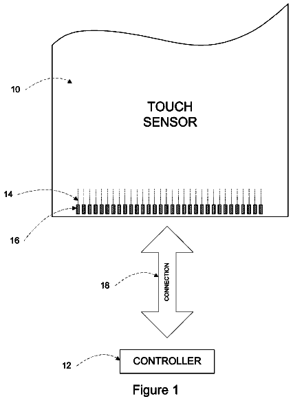
FIG. 1 illustrates an exemplary computing system capable of reducing stylus tip wobble according to examples of the disclosure.
FIGS. 2A and 2B illustrate an exemplary mutual capacitance touch sensor panel that can be used to detect touch or hover (proximity) events according to examples of the disclosure.
FIGS. 3A and 3B illustrate examples of the disparity between actual position and calculated position as a stylus moves along one axis of a touch sensor panel according to examples of the disclosure.
FIGS. 4A and 4B illustrate example signal profiles as a stylus moves along an axis of a touch sensor panel according to examples of the disclosure.
FIGS. 5A and 5B illustrate various signal profiles corresponding to various electrode configurations and levels of wobble error correlating with the signal profiles according to examples of the disclosure.
FIG. 6 illustrates an exemplary touch sensor panel system in which sense electrodes are in a signal-diffusing configuration according to examples of this disclosure.
FIG. 7 illustrates an exemplary non-signal-diffusing configuration in which sense electrodes are electrically isolated according to examples of the disclosure.
FIG. 8A-8D illustrate exemplary signal-diffusing configurations in which sense electrodes are coupled together via diffusing resistors according to examples of this disclosure.
FIGS. 9A and 9B illustrate various signal profiles corresponding to electrodes in a non-signal-diffusing configuration, and various signal profiles corresponding to electrodes in signal-diffusing configuration according to examples of the disclosure.
FIGS. 10A and 10B illustrate the impact of series resistance and diffusing resistance on distribution of a signal according to examples of the disclosure.
FIG. 10C is a flowchart of a method for selecting resistance values for use in a touch sensor panel according to examples of the disclosure.
FIGS. 11A and 11B illustrate the details of the structure of a sense electrode in a signal-diffusing configuration according to examples of the disclosure.
FIGS. 12A-12D illustrate example systems that can implement the signal-diffusing configurations for reducing stylus tip wobble according to examples of the disclosure.
Detailed description
In the following description of examples, reference is made to the accompanying drawings which form a part hereof, and in which it is shown by way of illustration specific examples that can be practiced. It is to be understood that other examples can be used and structural changes can be made without departing from the scope of the disclosed examples.
A stylus can be used as an input device for some capacitive touch sensor panels. In some examples, the touch sensor panel can have errors in position detection, referred to herein as wobble error, when a stylus is positioned between two of a plurality of sense electrodes. In some cases, wobble error can correlate to the signal profile between the stylus and electrodes within the touch sensor panel. Specifically, signal profiles which are narrower (i.e., less linear) can correlate to higher wobble error, while signal profiles which are widened within a range (i.e., to be more linear) can correlate to lower wobble error. Accordingly, in some examples, sense electrodes can be configured such that the signal profile associated with each sense electrode is spread to be wider, and thus, more linear. In some configurations, adjacent sense electrodes can be coupled together via diffusing resistors, which can be configured to diffuse a portion of a received signal to adjacent electrodes. In some examples, the value of the diffusing resistors coupling adjacent electrodes can be selected based on a desired signal profile between the stylus and each adjacent electrode. In some examples, the value of the diffusing resistors coupling adjacent electrodes can be selected based on series resistances associated with each adjacent electrode. In some examples, series resistance can include a conductive trace resistance and a compensating resistance. In some examples, compensating resistances can be selected to compensate for variances between electrodes, for example, variances in conductive trace resistance or diffusing resistance. In some examples, compensating resistances can be selected such that series resistances associated with each electrode are substantially equal. It should be understood that although examples of the disclosure are discussed herein primarily in terms of a stylus, the examples of the disclosure are not so limited, but include other small objects, including small fingers, that can cause wobble error similar to a stylus.
FIG. 1 illustrates an exemplary computing system capable of reducing wobble according to examples of the disclosure. Computing system 100 can include one or more panel processors 102 , peripherals 104 , and panel subsystem 106 . Peripherals 104 can include, but are not limited to, random access memory (RAM) or other types of memory or storage, watchdog timers and the like. Panel subsystem 106 can include, but is not limited to, one or more sense channels 108 , channel scan logic (analog or digital) 110 and driver logic (analog or digital) 114 . In mutual capacitance touch sensor panel examples, the panel can be driven and sensed using separate drive and sense lines, as shown in FIG. 1 . However, in self capacitance touch sensor panel examples, the sense electrodes can be driven and sensed using the lines. Channel scan logic 110 can access RAM 112 , autonomously read data from sense channels 108 and provide control for the sense channels. In addition, channel scan logic 110 can control driver logic 114 to generate stimulation signals 116 at various phases that can be simultaneously applied to touch sensor panel 124 . In some examples, panel subsystem 106 , panel processor 102 and peripherals 104 can be integrated into a single application specific integrated circuit (ASIC).
In mutual capacitance sensing examples, touch sensor panel 124 can include a capacitive sensing medium having a plurality of drive lines and a plurality of sense lines, although other sensing media can also be used. The drive and sense lines can be formed from a transparent conductive medium such as Indium Tin Oxide (ITO) or Antimony Tin Oxide (ATO), although other transparent and non-transparent materials such as copper can also be used. The drive and sense lines can be formed on a single side of a substantially transparent substrate, on opposite sides of the substrate, or on two separate substrates separated by dielectric material. Each intersection of drive and sense lines can represent a capacitive sensing node and can be viewed as picture element (pixel) 126 , which can be particularly useful when touch sensor panel 124 is viewed as capturing an “image” of touch. (In other words, after panel subsystem 106 has determined whether a touch event has been detected at each touch sensor in the touch sensor panel, the pattern of touch sensors in the multi-touch panel at which a touch event occurred can be viewed as an “image” of touch (e.g., a pattern of fingers touching the panel).) The capacitance between the drive and sense lines and local system ground can appear as a stray capacitance Cstray, and the capacitance at the intersections of the drive and sense lines, i.e., the touch nodes, can appear as a mutual signal capacitance Csig between the drive and sense lines when the given drive line is stimulated with an alternating current (AC) signal. The presence of a finger or other object (such as a stylus) near or on the touch sensor panel can be detected by measuring changes to a signal charge present at the nodes being touched, which can be a function of Csig. Each sense line of touch sensor panel 124 can be coupled to a sense channel 108 in panel subsystem 106 . Touch sensor panel 124 can cover a portion or substantially all of a surface of a device.
In self capacitance sensing examples, touch sensor panel 124 can include a capacitive sensing medium having a plurality of sense electrodes. The sense electrodes can be formed from a transparent conductive medium such as ITO or ATO, although other transparent and non-transparent materials such as copper can also be used. The sense electrodes can be formed on a single side of a substantially transparent substrate, on opposite sides of the substrate, or on two separate substrates separated by dielectric material. In some examples, the sense electrodes can be viewed as picture element (pixel) 126 , which can be particularly useful when touch sensor panel 124 is viewed as capturing an “image” of touch. In other examples, the sense electrodes can be configured as elongated sense rows and/or sense columns. The capacitance between the sense electrodes and system ground can represent the self capacitance of those electrodes. The presence of a finger or other object (such as a stylus) near or on the touch sensor panel can be detected by measuring changes to the self capacitance of nearby sense electrodes. Each sense electrode of touch sensor panel 124 can be coupled to a sense channel 108 in panel subsystem 106 . Touch sensor panel 124 can cover a portion or substantially all of a surface of a device
In some examples, computing system 100 can also include a stylus as an input device. In some examples, the stylus can actively capacitively couple with the drive and/or sense lines of touch sensor panel 124 by, for example, transducing a signal from the stylus to the drive and/or sense lines. In some examples, the stylus can act as a passive input device in a mutual capacitance system, as described above. In some examples, the touch sensor panel 124 includes a conductive sensing media having a plurality of sense rows and a plurality of sense columns, or a plurality of sense electrodes. In these examples, a stylus can capacitively couple with the sense rows, sense columns, or sense electrodes.
Computing system 100 can also include host processor 128 for receiving outputs from panel processor 102 and performing actions based on the outputs that can include, but are not limited to, moving one or more objects such as a cursor or pointer, scrolling or panning, adjusting control settings, opening a file or document, viewing a menu, making a selection, executing instructions, operating a peripheral device coupled to the host device, answering a telephone call, placing a telephone call, terminating a telephone call, changing the volume or audio settings, storing information related to telephone communications such as addresses, frequently dialed numbers, received calls, missed calls, logging onto a computer or a computer network, permitting authorized individuals access to restricted areas of the computer or computer network, loading a user profile associated with a user's preferred arrangement of the computer desktop, permitting access to web content, launching a particular program, encrypting or decoding a message, and/or the like. Host processor 128 can also perform additional functions that may not be related to panel processing, and can be coupled to program storage 132 and display device 130 such as an LCD display for providing a UI to a user of the device. Display device 130 together with touch sensor panel 124 , when located partially or entirely under the touch sensor panel, can form a touch screen.
In some examples, touch sensor panel 124 and display device 130 together can form an integrated touch screen in which touch sensing circuit elements of the touch sensing system (e.g., sense electrodes) can be integrated into the display pixel stackups of display device 130 . The circuit elements in an integrated touch screen can include, for example, elements that can exist in LCD or other displays, such as one or more pixel transistors (e.g., thin film transistors (TFTs)), gate lines, data lines, pixel electrodes and common electrodes. It is noted that circuit elements are not limited to whole circuit components, such as a whole capacitor, a whole transistor, etc., but can include portions of circuitry, such as only one of the two plates of a parallel plate capacitor. In some configurations, each common electrode in an integrated touch screen can serve as a multi-function circuit element that can operate as display circuitry of the display system of the touch screen and can also operate as elements of the touch circuitry of the touch sensing system. Specifically, each common electrode can operate as a common electrode of the display circuitry of the touch screen (e.g., during a display phase), and can also operate as a common electrode (i.e., a sense electrode) of the touch circuitry of the touch screen (e.g., during a touch sensing phase). It should be understood that a display phase and a touch sensing phase of an integrated touch screen may be operated at the same time, e.g., partially or completely overlapping, or the display phase and touch sensing phase may operate at different times.
In general, each of the touch sensing circuit elements may be either a multi-function circuit element that can form part of the touch circuitry and can perform one or more other functions, such as forming part of the display circuitry, or may be a single-function circuit element that can operate as touch circuitry only. Similarly, each of the display circuit elements may be either a multi-function circuit element that can operate as display circuitry and perform one or more other functions, such as operating as touch circuitry, or may be a single-function circuit element that can operate as display circuitry only. Therefore, in some examples, some of the circuit elements in the display pixel stackups can be multi-function circuit elements and other circuit elements may be single-function circuit elements. In other examples, all of the circuit elements of the display pixel stackups may be single-function circuit elements.
Note that one or more of the functions described above can be performed by firmware stored in memory (e.g., one of the peripherals 104 in FIG. 1 ) and executed by panel processor 102 , or stored in program storage 132 and executed by host processor 128 . The firmware can also be stored and/or transported within any non-transitory computer-readable storage medium for use by or in connection with an instruction execution system, apparatus, or device, such as a computer-based system, processor-containing system, or other system that can fetch the instructions from the instruction execution system, apparatus, or device and execute the instructions. In the context of this document, a “non-transitory computer-readable storage medium” can be any medium (excluding a signal) that can contain or store the program for use by or in connection with the instruction execution system, apparatus, or device. The non-transitory computer readable medium storage can include, but is not limited to, an electronic, magnetic, optical, electromagnetic, infrared, or semiconductor system, apparatus or device, a portable computer diskette (magnetic), a random access memory (RAM) (magnetic), a read-only memory (ROM) (magnetic), an erasable programmable read-only memory (EPROM) (magnetic), a portable optical disc such a CD, CD-R, CD-RW, DVD, DVD-R, or DVD-RW, or flash memory such as compact flash cards, secured digital cards, USB memory devices, memory sticks, and the like.
The firmware can also be propagated within any transport medium for use by or in connection with an instruction execution system, apparatus, or device, such as a computer-based system, processor-containing system, or other system that can fetch the instructions from the instruction execution system, apparatus, or device and execute the instructions. In the context of this document, a “transport medium” can be any medium that can communicate, propagate or transport the program for use by or in connection with the instruction execution system, apparatus, or device. The transport readable medium can include, but is not limited to, an electronic, magnetic, optical, electromagnetic or infrared wired or wireless propagation medium.
FIG. 2A symbolically illustrates an exemplary mutual capacitance touch sensor panel that can be used to detect touch or hover (proximity) events according to examples of the disclosure. In some mutual capacitance examples, touch sensor panel 200 can include an array of touch nodes 206 formed at the crossing points of row electrodes (e.g., drive lines) 201 a and column electrodes (e.g., sense lines) 202 a , although as discussed above, it should be understood that other drive and sense configurations can be used. A stylus can include an electrode configured to alter the capacitive coupling between a crossing row electrode and column electrode. Each of the column electrodes 202 can output its capacitance readings to one or more touch sensing circuits, which can be used to detect a touch or hover event.
The distance between each adjacent touch node in the same row can be a fixed distance, which can be referred to as the pitch P 1 for column electrodes. The distance between each adjacent touch node in the same column can be a fixed distance, which can be referred to as the pitch P 2 for row electrodes. In some examples, the pitch for row electrodes and column electrodes can be the same, but in other examples, P 1 and P 2 can be different.
During a mutual capacitance scan, one or more drive rows 201 a can be stimulated to drive the touch sensor panel 200 . Touch nodes 206 can have a mutual capacitance Cm at the touch nodes 206 when there is no object touching or hovering over touch nodes 206 . When an object touches or hovers over the touch node 206 (e.g. a stylus), the mutual capacitance Cm can be reduced by ΔCm, i.e., (Cm−ΔCm), corresponding to the amount of charge shunted through the object to ground. This mutual capacitance change can used to detect a touch or hover event and its location.
FIG. 2B symbolically illustrates an exemplary mutual capacitance touch sensor panel operable with an active stylus according to examples of the disclosure. In some mutual capacitance examples, an active stylus can generate stimulation signals (effectively operating as a drive electrode), and column electrodes 202 b and row electrodes 201 b can effectively operate as sense electrodes. During a stylus scan, one or more stimulation signals can be injected by stylus 208 into the touch sensor panel and can cause mutual capacitive coupling Cmr between the stylus 208 and the row traces 201 b and capacitive coupling Cmc between the stylus 208 and the column traces 202 b . The capacitance Cmr and Cmc can be transmitted to one or more touch sensing circuits for processing. In some examples, row traces 201 b and column traces 202 b can correspond to row electrodes 201 a and sense columns 202 a , however, during the stylus scan, stimulation signals are not applied to row electrodes 201 apart from signals generated by the active stylus. Additionally, in some examples, the touch sensor panel can include a stylus scan, a row scan, and a column scan, which can each operate as set forth above.
In some self capacitance examples, touch sensor panel 200 can include a plurality of sense electrodes (touch nodes). In some examples, the sense electrodes can be configured as elongated sense rows 201 and/or sense columns 202 . In other examples each sense electrode can be electrically isolated from the other sense electrodes and configured to represent a particular x-y location (e.g. touch node 206 ) on the panel. Such a touch screen can be referred to as a pixelated self-capacitance touch screen. A stylus can include an electrode configured to capacitively couple to a sense electrode. Each of the sense electrodes can output its capacitance readings to one or more touch sensing circuits, which can be used to detect a touch or hover event.
In some cases, an object, such as a stylus, may touch or hover at a position not directly over a touch node 206 , but in between two touch nodes 206 . For example, a stylus may touch or hover at a position between two row electrodes 201 , between two column electrodes 202 , or both. In these examples, the signal sensed at a plurality of touch nodes 206 may be used to estimate the location of the touch or hover event. In some examples, a centroid estimation algorithm can calculate the location of the touch or hover event using the signal sensed at the plurality of touch nodes 206 . For example, the position of a stylus on a touch sensor panel along an x-axis can be calculated by computing a weighted centroid defined in equation (1):
x calc = .Math. i = - N N x i S i .Math. i = - N N S i ( 1 )
where x.sub.calc can be the calculated position along the x-axis, S.sub.i can be the signal measured at the i.sup.th electrode, such as a sense electrode, along the x-axis, and x.sub.i can be the position of the i.sup.th electrode along the x-axis. It is to be understood that the centroid estimation algorithm defined in equation
is given only as an example, and the configurations described herein need not be limited to such examples. Instead, the calculation of a touch or hover location of an object can be accomplished using any appropriate method.
Ideally, as an object such as a stylus traverses between two touch nodes, the calculated position of the stylus on the touch screen and the actual position of the stylus should be the same. In reality, the calculated position may be different from the actual position due to limitations in the circuit configuration and the position estimation algorithms used. Errors resulting from the disparity between calculated position and actual position as an object moves along a touch sensor panel can be referred to as wobble error.
It can be useful to consider wobble error in the context of a stylus moving along a single axis of a touch sensor panel without diffusing resistors. This concept is illustrated by example in FIGS. 3A and 3B . FIGS. 3A and 3B illustrate examples of the disparity between actual position and calculated position as an object, such as a stylus, moves along an x-axis of a customary touch sensor panel (e.g., a touch panel without diffusing resistors) according to examples of the disclosure. FIG. 3A illustrates a plot of the calculated position of the stylus versus the actual position of the stylus when calculating position by using a weighted centroid algorithm including a subset of the electrodes (e.g., five electrodes) along an x-axis. In an ideal case, where calculated position and actual position are the same, the plot can be a straight line at a 45 degree angle. However, because of non-idealities in the coupling between the stylus and the touch sensor panel and the algorithm used to calculate stylus position, there can be non-ideal results that can appear as a wobble in the plot of FIG. 3A as the stylus moves between electrodes along the x-axis. In other words, the signal coupling between the stylus and touch sensor panel and the calculated position metric can introduce an error in calculated position (discrepancy with actual position) that can cause a wobble to be displayed when plotting the actual versus calculated position.
FIG. 3B illustrates a plot of the error in position calculation versus the actual position when calculating position by taking a weighted centroid including a subset of the electrodes (e.g., five electrodes) along an x-axis. The oscillation of the error plot can be representative of the wobble due to remaining error in the position calculation in a customary touch panel (e.g., a touch panel without diffusing resistors).
It should be noted that the scope of this disclosure can extend beyond the context of an active stylus coupling to sense electrodes, however, the examples of this disclosure focus on a stylus-sense electrode configuration for ease of description. FIGS. 3A and 3B relate to calculating position using a subset of the electrodes, however, it should be understood that the position could be calculated using any number of electrodes, including all of the electrodes in a touch sensor panel. Moreover, although FIGS. 3A and 3B are described with reference to the x-axis, in some examples, similar effects can be observed when moving the stylus across the touch sensor panel along the y-axis.
It can be useful to discuss the characteristics of the electrode configuration of a touch sensor panel in terms of the signal profile between a stylus and an electrode. This concept is explained by example with reference to FIGS. 4A and 4B . FIGS. 4A and 4B relate to an example signal profile in an x-axis of an example electrode 411 having a pitch with a distance D 1 as shown. As shown in FIG. 4A , an object, such as a stylus 421 , can be at a distance above an electrode 411 and moved in an x-direction across electrode 411 . At each point along the x-axis, a signal coupling Csig exists between the stylus and the electrode, which varies as the stylus moves from the midpoint M of electrode 411 . FIG. 4B illustrates a plot of an example signal profile, which can correlate to the signal Csig sensed on electrode 411 from stylus 421 as the stylus is moved in the x-direction. In some examples, such as when the stylus 421 is an active stylus, the signal Csig may represent a signal transduced by the stylus on the electrode. In some examples, the signal Csig may correspond to a self-capacitance of an object detected by the electrode or a change in mutual capacitance between a drive electrode and sense electrode. The x-axis of the plot in FIG. 4B can correlate to the position of the stylus in the x-axis relative to a midpoint M of an electrode 411 , and the y-axis of the plot in FIG. 4B can correlate to a normalized signal measurement at each x-position along the x-axis. The midpoint M of the x-axis of the plot in FIG. 4B can correspond to the midpoint M of electrode 411 shown in FIG. 4A . As shown in FIGS. 4A and 4B , the signal level can have a maximum value 423 when the stylus is at the midpoint of electrode 411 , and the signal level can decrease as the stylus traverses the x-axis away from the midpoint. In some examples, the signal profile can be non-linear. As discussed in more detail below, the signal profile between a stylus and an electrode can vary greatly based on a variety of factors including, for example, the circuit configuration of the electrodes.
In some examples, the wobble error of a touch sensor panel can correlate with the signal profile between a stylus and electrodes formed on the touch sensor panel. FIGS. 5A and 5B illustrate the correlation between three different example signal profiles 531 - 533 and the wobble error 541 - 543 associated with each of the example signal profiles. FIG. 5A illustrates plots of three example signal profiles 531 , 532 and 533 . As described above with reference to FIGS. 4A and 4B , each signal profile can represent a signal Csig sensed on an electrode 411 from a stylus 421 as the stylus is moved in an x-direction. Each of the signal profiles 531 , 532 and 533 in FIG. 5A can correspond to three hypothetical electrode configurations (not shown) A, B and C, each indicated by a different line pattern. Electrode configurations A-C can differ, for example, in electrode shape or circuit configuration.
FIG. 5B illustrates three example plots of the error in position calculation versus the actual position (i.e., wobble error) when calculating position of a stylus by taking a weighted centroid including a set of electrodes along an x-axis, with each error plot 541 , 542 and 543 corresponding to a set of electrodes with electrode configurations A, B, and C, respectively. FIG. 5B is similar to the plot of FIG. 3B , however, unlike the plot in FIG. 3B , which has an x-axis spanning the length of the touch sensor panel, the x-axis of FIG. 5B spans only the distance D 1 (e.g., the distance of the pitch) immediately surrounding a single electrode as shown. In some examples, the single oscillation in the error plots 541 , 542 and 543 shown in FIG. 5B can be similar to one of the many oscillations shown in FIG. 3B . For clarity, each of the example electrode configurations A-C in FIGS. 5A and 5B are assumed to have an equal pitch and midpoint.
In some examples, if a signal profile is very non-linear, position estimation algorithms, such as that listed in equation (1), can produce higher wobble error when a stylus is positioned between touch nodes. In the example of FIGS. 5A and 5B , an electrode configuration A can correspond to signal profile 531 and wobble error plot 541 . As shown in FIG. 5A , the shape of signal profile 531 corresponding to electrode configuration A is the least “spread” of signal profiles 531 - 533 . In other words, signal profile 531 is the least linear signal profile as a stylus is moved away from the peak. As shown in FIG. 5B , error plot 541 corresponding to electrode configuration A has the most wobble error of the error plots 541 - 543 . FIG. 5A also illustrates that the shape of signal profile 532 corresponding to electrode configuration B is more linear than signal profile 531 . As shown in FIG. 5B , error plot 542 corresponding to electrode configuration B has less wobble error than error plot 541 corresponding to electrode configuration A. FIG. 5A further illustrates that the shape of signal profile 533 corresponding to electrode configuration C is the most linear of signal profiles 531 - 533 , and its corresponding error plot 543 in FIG. 5B has the least wobble error of error plots 544 - 543 . Thus, as illustrated in these examples, electrode configurations with more linear signal profiles are correlated with lower wobble error.
The configurations and plots represented in FIGS. 5A and 5B are presented only as examples of how a more linear signal profile can be correlated with lower wobble error, and should not be understood to represent specific values or scale. It should be understood that wobble error of a touch sensor panel can be determined by other factors in addition to configuration of the electrodes in the touch sensor panel, such as, for example, position calculation algorithms used, stylus shape, and electrode pitch. Moreover, the solutions discussed in this disclosure can apply to configurations different from those discussed with respect to FIGS. 5A and 5B , including configurations of mutual capacitance, self-capacitance, and configurations wherein the touch object is not a stylus.
As discussed above, electrodes having a more linear signal profile can correlate to a lower wobble error. Therefore, it can be beneficial to configure each electrode in a touch sensor panel to have a more linear signal profile, by, for example, spreading the signal profile associated with each electrode outwardly toward adjacent electrodes. Thus, in some examples, it can be beneficial to couple adjacent electrodes together in signal-diffusing configurations using diffusing resistors. These signal-diffusing configurations will now be discussed below with reference to FIGS. 6-12 .
FIG. 6 illustrates a simplified diagram of an exemplary touch sensor panel system 600 including a plurality of electrodes 611 - 619 , touch sensing circuitry 621 , and a plurality of conductive traces 630 coupling electrodes to the touch sensing circuitry 621 . Electrodes can correspond, for example, to electrodes in a row electrode 201 or column electrode 202 as shown in FIG. 2A . In some examples, a plurality of diffusing resistors can be coupled between one or more electrodes in a signal-diffusing configuration. For example, in FIG. 6 , diffusing resistor 641 can be coupled between electrodes 611 and 612 . In some examples, series resistances Rs (represented conceptually as boxes with dashed lines) can be coupled between one or more electrodes and touch sensing circuitry 621 . Each of the series resistances Rs can represent one of a plurality of compensating resistances Rc (corresponding to resistors 661 - 669 ) and one of a plurality of trace resistances Rt. Touch sensing circuitry 621 can perform touch position estimation based on the signals detected by one or more of the plurality of sense electrodes, as discussed above with reference to FIG. 2A . For ease of description, only nine electrodes 611 - 619 and corresponding components are shown, however, it is understood that the scope of this disclosure includes touch sensor panels with more than nine sense electrodes as well as other supporting circuitry not shown in FIG. 6 . It should be noted that although the examples of this disclosure focus on diffusing resistors, other diffusing configurations are contemplated within the scope of this disclosure, which can include, for example components such as inductors, capacitors, additional resistors, etc. Moreover, in some cases, components within diffusing configurations can be coupled to switches to control their function. In some examples, resistances such as diffusion resistors and/or series resistances may comprise resistances inherent to circuit components (e.g., not discrete or intentional resistors).
In some examples, electrodes 611 - 619 can be composite electrodes, including a plurality of component electrodes (e.g., prongs) extending along the length of the sense electrode. FIG. 7 illustrates an exemplary non-diffusing electrode configuration, in which each composite electrode 711 - 713 is configured to be electrically isolated from one another. Composite electrodes 711 - 713 can each include a plurality of prongs 720 . Composite electrodes 711 - 713 shown in FIG. 7 each include three prongs, though other examples may have more or fewer prongs than the electrodes shown in FIG. 7 . The signal profile of the configuration of FIG. 7 is discussed in detail with reference to FIG. 9A below.
As explained above with reference to FIGS. 5A and 5B , it can be beneficial to diffuse the signal detected on a sense electrode to adjacent electrodes such that the signal profile associated with the electrode is spread, and thus more linear. This spreading of signal profile can correlate to lower wobble error associated with the touch sensor panel. FIGS. 8A-8D illustrate four exemplary diffused electrode configurations which spread the signal profile associated with each electrode to be wider, and thus, more linear. The signal profiles for each of the electrode configurations in FIGS. 8A-8B are discussed in more detail with reference to FIG. 9B below.
FIG. 8A illustrates example sense electrodes in an exemplary signal-diffusing configuration, in which each of the composite electrodes 811 - 813 is coupled to an adjacent electrode via one of a plurality of diffusing resistors 841 - 842 . The values and operation of diffusing resistors 841 - 842 will be discussed in more detail with reference to FIGS. 9A-9B below, though it should be noted that not every electrode may be coupled to an adjacent electrode in some examples. Like the electrode configuration illustrated in FIG. 7 , the electrodes shown in FIG. 8A can each include three prongs 820 , though more or less prongs may be present in other configurations. As shown, each prong 820 within a single electrode can be directly coupled to an adjacent prong. Each composite electrode 811 - 813 can have a corresponding series resistance Rs. Series resistance Rs can be analogous to the series resistance Rs discussed with reference to FIG. 6 , and may include a trace resistance Rt and a compensating resistance Rc. For purposes of this discussion, series resistances Rs associated with each electrode 811 - 813 are assumed to be equal. The values and operation of series resistances Rs, including trace resistance Rt and compensating resistance Rc, will be discussed in more detail below.
The description continues in the full USPTO document.
 Lapsed, fee not paid8 drawings