Technical field
The present application relates to a liquid crystal alignment film, a manufacturing method of the liquid crystal alignment film, an optical filter, and a display device.
Background
A stereoscopic image display device is a display device capable of transmitting three-dimensional information to an observer.
Methods for displaying stereoscopic images may include, for example, methods that use glasses and methods that don't use glasses. Also, the methods using glasses may be classified into methods using polarizing glasses and methods using LC shutter glasses, and the methods that don't use glasses may be classified into stereoscopic/multi-view point binocular disparity methods, volumetric methods, holographic methods, and the like. Patent Document 1 (Japanese Patent Publication No. 2005-049865), Patent Document 2 (Korean Patent No. 0967899) and Patent Document 3 (Korean Patent Publication No. 2010-0089782) describe optical elements which can be efficiently used in a stereoscopic image display process. DETAILED DESCRIPTION Technical Object
This application provides a liquid crystal alignment film, a manufacturing method of the liquid crystal alignment film, an optical filter, and a display device. Technical Solution
This application relates to a liquid crystal alignment film. A liquid crystal alignment film according to one embodiment may include a surface having a liquid crystal alignment ability and a groove. In the present specification, the term “surface having a liquid crystal alignment ability” means a surface having an ability to induce alignment of a liquid crystal layer adjacent to the surface. In one embodiment, the groove may be present directly in the surface having a liquid crystal alignment ability, or may be present at a certain region of an upper part or a lower part of the surface. According to one embodiment, the groove may have a width in the range of, for example, 5 μm to 300 μm and a depth in the range of, for example, 0.5 μm to 5 μm.
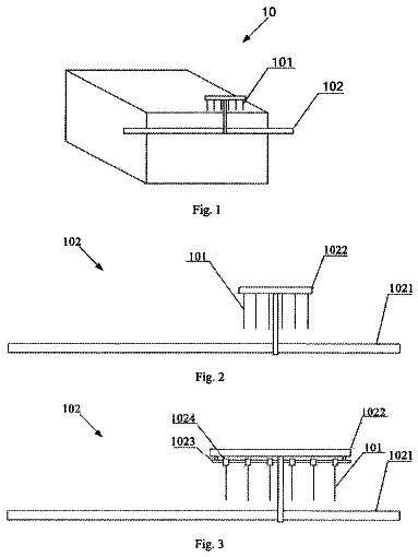
FIGS. 1 to 3 show schematics of illustrative embodiments of the liquid crystal alignment films 1 . In one embodiment, the liquid crystal alignment film 1 may have a structure in which a groove 102 is present directly in a surface having a liquid crystal alignment ability 101 as illustrated in FIG. 1 . In another embodiment, the liquid crystal alignment film 1 may have a structure in which a liquid crystal alignment layer 104 is formed on a surface of an underlying layer 103 including the groove 102 as illustrated in FIG. 2 . In this case, the liquid crystal alignment film may further include a substrate layer 105 formed on the side of the underlying layer 103 , where the liquid crystal alignment layer 104 is not formed. In another embodiment, the liquid crystal alignment film 1 may further include a substrate layer 105 as illustrated in FIG. 3 , and in this case, the liquid crystal alignment film 1 may have a structure in which the liquid crystal alignment layer 104 is formed directly on a surface of the substrate layer 105 including the groove 102 .
The surface having a liquid crystal alignment ability can be formed by a typical alignment layer publicly known in the art. As the alignment layer, conventional alignment layers known in the field may be used. For example, a photo-alignment layer, of which an alignment may be determined by dimerization, fries rearrangement or cis-trans isomerization reaction induced by an irradiation with a linearly polarized light, and which then can induce an alignment in a liquid crystal layer adjacent thereto by the determined alignment, a polymer layer such as a rubbed polyimide layer or an alignment layer in which a plurality of patterned grooves are formed such as an alignment layer formed by an imprinting method such as a nano imprinting method may be exemplified.
In one embodiment, the alignment layer may be a photo-alignment layer. The photo-alignment layer may be formed by using, for example, a photo-alignment compound. The photo-alignment compound refers to a compound capable of inducing alignment of an adjacent liquid crystal compound through alignment in a certain direction by irradiation of light, for example, irradiation of linearly polarized light.
The photo-alignment compound may contain, for example, a photosensitive moiety. There have been publicly known various photo-alignment compounds which can be used for alignment of a liquid crystal compound. As the photo-alignment compound, for example, a compound aligned by trans-cis photoisomerization, a compound aligned by photo-destruction such as chain scission or photo-oxidation, a compound aligned by photo-crosslinking such as [2+2] cycloaddition, [4+4] cycloaddition, or photodimerization, or photopolymerization, a compound aligned by photo-Fries rearrangement, a compound aligned by ring opening/closure, or the like may be used. The compound aligned by trans-cis photoisomerization may include, for example, an azo compounds such as a sulfonated diazo dye or an azo polymer, or stilbene compounds. The compound aligned by photo-destruction may include, for example, cyclobutane-1,2,3,4-tetracarboxylic dianhydride, aromatic polysilane or polyester, polystyrene, polyimide, or the like. Further, the compound aligned by photo-crosslinking or photopolymerization may include, for example, a cinnamate compound, a coumarin compound, a cinnamamide compound, a tetrahydrophthalimide compound, a maleimide compound, a benzophenone compound, or a diphenylacetylene compound, a compound including a chalconyl moiety (hereinafter, referred to as “chalcone compound”) or a compound including an anthracenyl moiety (hereinafter, referred to as “anthracenyl compound”) as a photosensitive moiety. The compound aligned by photo-Fries rearrangement may include aromatic compounds such as a benzoate compound, a benzoamide compound, methacrylamidoaryl methacrylate, and the like. The compound aligned by ring opening/closure may include, for example, a compound aligned by ring opening/closure in a ring opening/closure reaction of a [4+2] π-electronic system such as a spiropyran compound, but it is not limited thereto.
The photo-alignment compound may be, for example, a monomolecular compound, a monomeric compound, an oligomeric compound, or a polymeric compound, or a blend of the photo-alignment compound and a polymer. The oligomeric or polymeric compound may have a moiety induced from the above-described photo-alignment compound or the above-described photosensitive moiety in a main chain or at a side chain.
Examples of the polymer which may have a moiety induced from a photo-alignment compound or a photosensitive moiety or may be blended with the photo-alignment compound may include polynorbonene, polyolefin, polyarylate, polyacrylate, poly(meth)acrylate, polyimide, poly(amic acid), polymaleinimide, polyacrylamide, polymethacrylamide, polyvinyl ether, polyvinyl ester, polystyrene, polysiloxane, polyacrylnitrile, or polymethacrylnitrile, but it is not limited thereto.
Representative examples of the polymer which may be contained in the photo-alignment compound may include polynorbonene cinnamate, polynorbonene alkoxy cinnamate, polynorbonene allyloyloxy cinnamate, polynorbonene fluorinated cinnamate, polynorbornene chlorinated cinnamate, or polynorbornene dicinnamate, but it is not limited thereto.
If the photo-alignment compound is the polymeric compound, the compound may have a number average molecular weight in the range of, for example, from about 10,000 g/mol to about 500,000 g/mol, but it is not limited thereto.
A method of forming a photo-alignment layer using the above-described photo-alignment compound is not particularly limited and may employ a method publicly known in the art.
In one embodiment, the liquid crystal alignment film may further include a substrate layer and a surface having a liquid crystal alignment ability may be formed on the substrate layer. FIGS. 2 and 3 show schematics of illustrative embodiments of the liquid crystal alignment films including a substrate layer. As described above, the liquid crystal alignment film may have a structure in which the underlying layer 103 including the groove 102 and the liquid crystal alignment layer 104 are formed in sequence on the substrate layer 105 as illustrated in FIG. 2 , or may have a structure in which the groove 102 is formed directly in the substrate layer 105 and the liquid crystal alignment layer 104 is formed thereon as illustrated in FIG. 3 .
As the substrate layer, for example, a glass substrate or a plastic substrate typically used in manufacturing optical elements may be used. Examples of the plastic substrate layer may include a cellulose substrate including triacetyl cellulose (TAC) or diacetyl cellulose (DAC); a cyclo olefin polymer (COP) substrate such as a norbornene derivative; an acryl substrate such as poly(methyl methacrylate) (PMMA); a polycarbonate (PC) substrate; a polyolefin substrate such as polyethylene (PE) or polypropylene (PP); a polyvinyl alcohol (PVA) substrate; a polyethersulfone (PES) substrate; a polyetheretherketone (PEEK) substrate; a polyetherimide (PEI) substrate; a polyethylene naphthalate (PEN) substrate; a polyester substrate such as polyethylene terephthalate (PET); a polyimide (PI) substrate; a polysulfone (PSF) substrate; or a fluororesin substrate such as an amorphous fluororesin, but is not limited thereto. According to an exemplary embodiment, a cellulose substrate such as a TAC substrate may be used.
The plastic substrate layer may have a refractive index lower than that of a liquid crystal layer to be described below. A refractive index of an exemplary substrate layer may be in the range of about 1.33 to about 1.53. If the substrate layer has a refractive index lower than that of the liquid crystal layer, it is useful in improving brightness, preventing reflection, and improving a contrast characteristic. Further, for example, the plastic substrate layer may be optically isotropic or anisotropic.
In one embodiment, the substrate layer may further contain a UV blocking agent or a UV ray absorbent. If a UV blocking agent or a UV ray absorbent is contained in the substrate layer, deterioration of the liquid crystal layer caused by UV rays can be prevented. Examples of the UV blocking agent or the UV ray absorbent may include an organic material such as a salicylic acid ester compound, a benzophenone compound, an oxybenzophenone compound, a benzotriazol compound, a cyanoacrylate compound, or a benzoate compound, or an inorganic material such as zinc oxide or nickel complex salt. A content of the UV blocking agent or the UV ray absorbent in the substrate layer is not particularly limited and may be selected appropriately for purpose of the effect. For example, in manufacturing the plastic substrate layer, the UV blocking agent or the UV ray absorbent may be contained in an amount of about 0.1 wt % to about 25 wt % with respect to the weight of a main material of the substrate layer.
The substrate layer may have, for example, a monolayer structure or a multilayer structure and a monolayer structure may be selected for providing an element having a smaller thickness. A thickness of the substrate layer is not particularly limited and may be adjusted appropriately for purpose of use.
In one embodiment, the groove included in the liquid crystal alignment film may have, for example, a width (W) and a depth (D) as illustrated in FIG. 2 . For example, the groove included in the liquid crystal alignment film may have a width in the range of 5 μm to 300 μm, from 50 μm to 250 μm, or from 100 μm to 200 μm, and a depth in the range of 0.5 μm to 5 μm, from 1 μm to 4.5 μm, from 1.5 μm to 4.0 μm, from 2.0 μm to 3.5 μm, or from 2.5 μm to 3.0 m. If the width and the depth of the groove of the liquid crystal alignment film satisfy the above-described ranges, when the liquid crystal alignment film is included in an optical filter, which will be described below, to be used in a display device, brightness of the display device can be improved.
In one embodiment, the liquid crystal alignment film may include two or more grooves, and the grooves may have stripe shapes extending in the same direction respectively, and may be separately arranged from each other. In another embodiment, the grooves may be separately arranged from each other in a lattice pattern. However, arrangement of the grooves is not limited thereto and may employ other various designs.
In one embodiment, the grooves included in the liquid crystal alignment film may have, for example, a pitch P between the grooves separately arranged from each other as illustrated in FIG. 2 . The grooves included in the liquid crystal alignment film may have a pitch P between the grooves separately arranged from each other in the range of, for example, from 50 μm to 1000 μm. If the pitch between the grooves of the liquid crystal alignment film satisfies the above-described range, when the liquid crystal alignment film is included in an optical filter, which will be described below, to be used in a display device, brightness of the display device can be improved.
In one embodiment, the grooves of the liquid crystal alignment film may be filled with a light blocking material, a light reflecting material, or a light scattering material. For example, the grooves of the liquid crystal alignment film may contain one or more of the above-described materials in a mixed state or in a state where the materials form layers distinguishable from each other.
FIGS. 4 to 6 show schematics of illustrative embodiments of the liquid crystal alignment films comprising the liquid crystal alignment layer 104 present on the surface of the underlying layer 103 including the grooves, wherein the grooves are filled with the above-described materials. FIG. 4 shows one embodiment where the grooves of the liquid crystal alignment film are filled with a light blocking material 106 , FIG. 5 shows one embodiment where the grooves of the liquid crystal alignment film are filled with the light blocking material 106 and another functional material such as a light reflecting material 107 , and FIG. 6 shows one embodiment where the grooves of the liquid crystal alignment film are filled with the light reflecting material 107 .
The light blocking material, the light reflecting material, or the light scattering material are not particularly limited in kind and may employ publicly-known materials. For example, the light blocking material may employ publicly-known light blocking or light absorbing ink without particular limitation. Examples of the ink may include carbon black ink or ink including inorganic pigment such as graphite or iron oxide, or organic pigment ink (black pigment ink) such as an azo-based pigment or a phthalocyanine-based pigment. For example, the light reflecting material may employ metallic ink, a cholesteric liquid crystal material, a birefractive material, or the like. For example, the light scattering material may employ silica particles or nanoparticles. Each of the light blocking material, the light reflecting material, and the light scattering material may be used alone or may be mixed with an appropriate binder and/or a solvent so as to fill the grooves. For example, if the liquid crystal alignment film is applied to an optical filter to be described below, light transmittance of the groove regions can be adjusted by adjusting a mixing amount or a kind of the pigment.
In one embodiment, the liquid crystal alignment film may include a first layer having a surface in which a groove has a width in the range of 5 μm to 300 μm and a depth in the range of 0.5 μm to 5 μm; and a liquid crystal alignment layer formed on the surface of the first layer. For example, the first layer may include the underlying layer 103 and the substrate layer 105 as illustrated in FIG. 2 , or may include the substrate layer 105 only as illustrated in FIG. 3 .
The substrate layer of the first layer may employ the same glass or plastic substrate layer described above with respect to the substrate layer, and the underlying layer of the first layer may employ, for example, any one selected from publicly-known resin layers without particular limitation. The resin layer may contain, for example, a room temperature-curable resin composition, a moisture-curable resin composition, a thermosetting resin composition, or an active energy ray-curable resin composition in a cured state. According to an exemplary embodiment, the resin layer may contain a thermosetting resin composition or an active energy ray-curable resin composition, or may contain an active energy ray-curable resin composition in a cured state. In explanation of a high hardness layer, the term “cured state” means a state where elements contained in each of the resin compositions go through a crosslinking reaction or a polymerization reaction, and thus, the resin composition is converted into a hardened state. Further, the room temperature-curable resin composition, the moisture-curable resin composition, the thermosetting resin composition, or the active energy ray-curable resin composition means a composition which can be induced to be in the cured state at room temperature, in the presence of adequate moisture, by application of heat, or by irradiation of active energy rays.
For example, a surface of the first layer may have a maximum height roughness of 1 μm or less, 0.8 μm or less, 0.6 μm or less, 0.4 μm or less, or 0.2 μm or less in state that the grooves are filled with the light blocking material, the light reflecting material, or the light scattering material. The maximum height roughness means a distance between a straight line passing through an uppermost point of an illumination curve and a straight line passing through a lowermost point of the illumination curve which are parallel to a central line in the illumination curve within a cutoff, and may be a value measured on a certain region having an area of 100 μm.sup.2 on the first layer. If the first layer of the liquid crystal alignment film satisfies the above-described range of the maximum height roughness, a height difference between the groove region filled with the light blocking material or the like and the other regions which are not filled can be reduced. Therefore, when a polarizing plate is attached to the liquid crystal alignment film, separation does not occur and thus can be usefully applied to manufacturing an integrated polarizing plate for an optical filter to be described later.
This application also relates to a manufacturing method of the liquid crystal alignment film.
In one embodiment, the liquid crystal alignment film can be manufactured by a method including: granting a liquid crystal alignment ability to a surface of a layer that includes a groove having a width in the range of 5 μm to 300 μm and a depth in the range of 0.5 μm to 5 μm.
In one exemplary embodiment, the granting of a liquid crystal alignment ability to a surface of a layer that includes a groove may be carried out by, for example, forming a first layer including a groove on the surface and forming a liquid crystal alignment layer on the first layer's surface including the groove. FIG. 7 shows a schematic of an illustrative embodiment of a manufacturing method of a liquid crystal alignment film. Referring to FIG. 7 , the liquid crystal alignment film can be manufactured by forming the underlying layer 103 , for example, a trench film, including a groove on the substrate layer 105 as shown in a step (a), filling the groove with the light blocking material 106 or the light blocking material 106 and the light reflecting material 107 as shown in a step (b), and forming the liquid crystal alignment layer 104 as shown in a step (c). Further, as described below, when the liquid crystal alignment film is applied to an optical filter, in addition to the steps (a), (b), and (c), a step (d) may be added to form a liquid crystal layer including a first region 201 and a second region 202 different from each other in a phase retardation property on the liquid crystal alignment layer 104 , so that an optical filter can be manufactured.
The forming of the groove in the first layer may be carried out by, for example, forming an concave-convex surface on the underlying layer. A method of forming the concave-convex surface on the underlying layer is not particularly limited, and for example, while a coating layer of a resin composition for forming the underlying layer is brought in contact with a mold having a targeted concave-convex structure, the resin composition may be cured, thereby forming the concave-convex structure. In another embodiment, forming the groove in the first layer may be carried out by, for example, forming the concave-convex surface on the substrate layer, and the concave-convex surface of the substrate layer may be formed by, for example, a printing method or a laser processing method.
The forming of the liquid crystal alignment layer on the first layer may be carried out by, for example, a method of forming and rubbing-aligning a polymer film such as polyimide on the first layer, a method of coating a photo-alignment compound and performing an alignment process through irradiation of linearly polarized light, or an imprint lithography such as nanoimprint lithography.
In another embodiment, the granting of a liquid crystal alignment ability to a surface of a layer that includes a groove may be carried out by forming a liquid crystal alignment layer and thereafter forming a groove on the surface of the liquid crystal alignment layer. The groove may be formed by, for example, a printing method or a laser processing method.
In one embodiment, the granting of a liquid crystal alignment ability may be carried out such that the liquid crystal alignment film can have a first alignment region and a second alignment region which have different alignment abilities from each other. In one embodiment, the liquid crystal alignment film may be manufactured such that the first alignment region and the second alignment region are formed in stripe shapes extending in the same direction and are alternately arranged adjacent to each other. In one embodiment, the liquid crystal alignment film may be manufactured such that the grooves present under the liquid crystal alignment layer can be overlapped with the first alignment region and the second alignment region on the border between the first alignment region and the second alignment region when observed from a direction of a normal line of the surface of the liquid crystal alignment film.
Further, the manufacturing method of the liquid crystal alignment film may further include filling the groove with the light blocking material, the light reflecting material, or the light scattering material before the liquid crystal alignment layer is formed. A method of filling the groove with the light blocking material, the light reflecting material, or the light scattering material is not particularly limited and may employ, for example, a printing method such as a screen printing method or a gravure printing method, or a selective ink jetting method.
This application also relates to an optical filter. In one embodiment, an optical filter may include a liquid crystal alignment film and a liquid crystal layer. The liquid crystal layer may be present on the liquid crystal alignment film. The above descriptions regarding the exemplary liquid crystal alignment film of the present invention can be equally applied to the liquid crystal alignment film, and the liquid crystal layer may include, for example, a first region and a second region different from each other in a phase retardation property.
For example, the optical filter may be a device configured to split incident light into two or more kinds of light different from each other in a polarization state. Such a device can be used for, for example, realizing a stereoscopic image.
The liquid crystal layer may include the first region and the second region which are different from each other in the phase retardation property. In the present specification, the expression “a first region and a second region are different from each other in the phase retardation property” may include, for example, a case where the first region and the second region have optical axes formed in directions identical to or different from each other and have phase retardation values different from each other and a case where the first region and the second region have the same phase retardation value and have optical axes formed in directions different from each other, when the first region and the second region have phase retardation properties.
In another embodiment, the expression “a first region and a second region different from each other in the phase retardation property” may include a case where any one region of the first region and a second region has a phase retardation property and the other region does not have a phase retardation property and is optically isotropic. In this case, both a region where the liquid crystal layer is formed and a region where the liquid crystal layer is not formed may be included. The phase retardation property of the first region or the second region can be controlled by adjusting, for example, an alignment state of a liquid crystal compound, a relationship of refractive indexes in the liquid crystal layer, or a thickness of the liquid crystal layer.
In one embodiment, the liquid crystal alignment film may include two or more grooves, and the two or more grooves may be formed in stripe shapes extending in the same direction and may be separately arranged from each other. In this case, the first region and the second region may be formed in stripe shapes extending in the same direction and may be alternately arranged adjacent to each other, and the grooves may be overlapped with the first region or the second region on the border between the first region and the second region when observed from a direction of a normal line of the surface of the liquid crystal alignment film. FIG. 8 illustrates an exemplary optical filter in which grooves 102 formed in a surface having a liquid crystal alignment ability 101 in a liquid crystal alignment film are arranged to be overlapped with a first region 201 and a second region 202 .
In another embodiment, the first region and the second region may be alternately arranged to be adjacent to each other in a lattice pattern. In this case, the first region and the second region may be alternately arranged to be adjacent to each other in a lattice pattern, and also, the grooves may be overlapped with the first region or the second region on the border between the first region and the second region when observed from the direction of the normal line of the surface of the liquid crystal alignment film.
In one embodiment, when the optical filer is used in a device that displays a stereoscopic image, any one of the first and second regions may refer to a region for controlling the polarization state of a signal for a left eye (hereinafter, referred to as “LG region”), and the other region may refer to a region for controlling the polarization state of a signal for a right eye (hereinafter referred to as “RG region”). In another embodiment, when the optical filer is used in a device that displays a stereoscopic image, the groove region filled with the light blocking material may refer to a light-penetration-controlling region (hereinafter, referred to as “TC region”).
In one embodiment, the two or more kinds of light different from each other in a polarization state and split by the liquid crystal layer including the first region and the second region may include two kinds of linearly polarized light having substantially vertical directions to each other, or may include left-circularly polarized light and right-circularly polarized light.
Unless otherwise defined in this specification, when terms such as vertical, horizontal, perpendicular, or parallel are used in definitions of angles, the terms refer to an angle being substantially vertical, horizontal, perpendicular, or parallel. For example, the terms include errors in consideration of manufacturing errors or variations. Therefore, the terms may include, for example, an error of less than about ±15°, an error of less than about ±10°, or an error of less than about ±5°.
In another embodiment, any one of the first and second regions may be a region through which incident light penetrates without rotating the polarization axis of the incident light, and the other region may be a region through which incident light penetrates while the polarization axis of the incident light is rotated in a direction perpendicular to the polarization axis of the incident light which penetrates through the one of the first and second regions. In this case, the regions of the liquid crystal layer including a polymerizable liquid crystal compound may be formed on only one of the first and second regions. The region in which the liquid crystal layer is not formed may be empty, or may be a region in which a glass or optically isotropic resin layer, or a resin film or sheet is formed.
In another embodiment, any one of the first and second regions may be a region through which incident light can penetrate when the incident light is converted into left-circularly polarized light, and the other region may be a region through which incident light can penetrate when the incident light is converted into right-circularly polarized light. In this case, the first and second regions have optical axes formed in different directions and have the same phase retardation value, or one of the first and second regions may be a region in which incident light may be phase-retarded by ¼ of a wavelength of the incident light, and the other region may be a region in which incident light may be phase-retarded by ¾ of a wavelength of the incident light.
In one embodiment, the first and second regions may have the same phase retardation value, for example, a value required to phase-retard incident light by ¼ of a wavelength of the incident light, and also have optical axes formed in different directions. The optical axes formed in the different directions may be, for example, at an angle of about 90°.
For example, the liquid crystal layer may have a difference between in-plane refractive indexes in a slow axis direction and in-plane refractive indexes in a fast axis direction in the range of 0.05 to 0.2, 0.07 to 0.2, 0.09 to 0.2, or 0.1 to 0.2. The in-plane refractive index in the slow axis direction may refer to a refractive index in a direction in which the maximum value of the refractive index is defined with respect to the plane of the liquid crystal layer, and the in-plane refractive index in the fast axis direction may refer to a refractive index in a direction in which the minimum value of the refractive index is defined with respect to the plane of the liquid crystal layer. Typically, the fast axis and slow axis in an optically anisotropic liquid crystal layer are formed vertically to each other. The refractive indexes may be measured with respect to light at a wavelength of 550 nm or 589 nm. The liquid crystal layer may also have a thickness of about 0.5 μm to about 2.0 μm or about 0.5 μm to about 1.5 μm. The liquid crystal layer satisfying the relationship of the refractive indexes and having the thickness may express a phase retardation property suitable for use in applications. The liquid crystal layer satisfying the relationship of the refractive indexes and having the thickness may be suitable for use in an optical filer for optical division.
The liquid crystal layer may be, for example, a photo-crosslinking layer or a photopolymerizable layer of a photo-crosslinking or photopolymerizable liquid crystal compound, respectively. In this technical field, various liquid crystal compounds having the above-described properties are publicly known and may include, for example, Reactive Mesogen (RM) of Merk or LG242 of BASF.
The liquid crystal layer may contain, for example, a multifunctional polymerizable liquid crystal compound and a monofunctional polymerizable liquid crystal compound. The polymerizable liquid crystal compounds may be contained in a polymerized form in the liquid crystal layer.
The term “multifunctional polymerizable liquid crystal compound” may refer to a compound that has a liquid crystalline property since it includes a mesogen backbone, and also has two or more polymerizable functional groups. According to one exemplary embodiment, the multifunctional polymerizable liquid crystal compound may include 2 to 10, 2 to 8, 2 to 6, 2 to 5, 2 to 4, 2 to 3, or 2 polymerizable functional groups.
The term “monofunctional polymerizable liquid crystal compound” may refer to a compound that has a liquid crystalline property since it includes a mesogen backbone, and has one polymerizable functional group.
Also, the expression “polymerizable liquid crystal compound contained in a polymerized form in a liquid crystal layer” may refer to a state where the liquid crystal compound is polymerized so as to form a liquid crystal polymer in the liquid crystal layer.
If the liquid crystal layer includes both of the multifunctional and monofunctional polymerizable compounds, the liquid crystal layer may have more excellent phase retardation properties, and the realized phase retardation properties, for example, the optical axis and a phase retardation value of the liquid crystal layer, may be stably maintained even under severe conditions.
According to one exemplary embodiment, the polymerizable liquid crystal compound may be a compound represented by the following Chemical Formula 1.
##str00001##
In Chemical Formula 1, A may be a single bond, —COO—, or —OCO—, and R.sub.1 to R.sub.10 may be each independently hydrogen, a halogen, an alkyl group, an alkoxy group, an alkoxycarbonyl group, a cyano group, a nitro group, —O-Q-P—, or a substituent represented by the following Chemical Formula 2, or a pair of two adjacent substituents among R.sub.1 to R.sub.5 or a pair of two adjacent substituents among R.sub.6 to R.sub.10 is joined together to form benzene substituted with —O-Q-P—, with the proviso that at least one of the R.sub.1 to R.sub.10 is —O-Q-P— or a substituent of Chemical Formula 2, or at least one pair of two adjacent substituents among R.sub.1 to R.sub.5 or among R.sub.6 to R.sub.10 is joined together to form benzene substituted with —O-Q-P—, where Q may be an alkylene group or an alkylidene group, and P may be a polymerizable functional group such as an alkenyl group, an epoxy group, a cyano group, a carboxyl group, an acryloyl group, a methacryloyl group, an acryloyloxy group, or a methacryloyloxy group.
##str00002##
In Chemical Formula 2, B may be a single bond, —COO—, or —OCO—, and R.sub.11 to R.sub.15 may be each independently hydrogen, a halogen, an alkyl group, an alkoxy group, an alkoxycarbonyl group, a cyano group, a nitro group or —O-Q-P—, or at least one pair of two adjacent substituents among R.sub.1 to R.sub.5 or among R.sub.6 to R.sub.10 is joined together to form benzene substituted with —O-Q-P— with the proviso that at least one of substituents R.sub.11 to R.sub.1 is —O-Q-P—, or at least one pair of two adjacent substituents among R.sub.11 to R.sub.1 is joined together to form benzene substituted with —O-Q-P—, where Q may be an alkylene group or an alkylidene group, and P may be a polymerizable functional group such as an alkenyl group, an epoxy group, a cyano group, a carboxyl group, an acryloyl group, a methacryloyl group, an acryloyloxy group, or a methacryloyloxy group.
In Chemical Formulas 1 and 2, the expression “two adjacent substituents are joined together to form benzene substituted with O-Q-P—” may refer to the two adjacent substituents being joined together so as to form a naphthalene backbone substituted with O-Q-P— as a whole.
In Chemical Formula 2, the mark “—” indicated on the left of the “B” may refer to the “B” being directly bound to the benzene of Chemical Formula 1.
In Chemical Formulas 1 and 2, the term “single bond” means that no atom is present in a site represented by the “A” or “B.” For example, if the “A” in Chemical Formula 1 is a single bond, the benzene disposed on both sides of the “A” may be directly bound to form a biphenyl structure.
In Chemical Formulas 1 and 2, the halogen may be, for example, chlorine, bromine, or iodine.
In Chemical Formulas 1 and 2, the term “alkyl group” may refer to a linear or branched alkyl group having 1 to 20 carbon atoms, 1 to 16 carbon atoms, 1 to 12 carbon atoms, 1 to 8 carbon atoms, or 1 to 4 carbon atoms; or a cycloalkyl group having 3 to 20 carbon atoms, 3 to 16 carbon atoms, or 4 to 12 carbon atoms. The alkyl group may be optionally substituted with one or more substituents.
Unless defined otherwise, the term “alkoxy group” as used in the present specification may refer to an alkoxy group having, for example, 1 to 20 carbon atoms, 1 to 16 carbon atoms, 1 to 12 carbon atoms, 1 to 8 carbon atoms, or 1 to 4 carbon atoms. For example, the alkoxy group may have a linear, branched, or cyclic structure. Also, the alkoxy group may be optionally substituted with one or more substituents.
Unless defined otherwise, the term “alkylene group” or “alkylidene group” as used in the present specification may refer to an alkylene group or alkylidene group having 1 to 12 carbon atoms, 4 to 10 carbon atoms, or 6 to 9 carbon atoms. The alkylene group or alkylidene group may have, for example, a linear, branched, or cyclic structure. Also, the alkylene group or alkylidene group may be optionally substituted with one or more substituents.
Unless defined otherwise, the term “alkenyl group” as used in the present specification may refer to an alkenyl group having 2 to 20 carbon atoms, 2 to 16 carbon atoms, 2 to 12 carbon atoms, 2 to 8 carbon atoms, or 2 to 4 carbon atoms. The alkenyl group may have a linear, branched, or cyclic structure. Also, the alkenyl group may be optionally substituted with one or more substituents.
Further, in Chemical Formulas 1 and 2, the “P” may be, for example, an acryloyl group, a methacryloyl group, an acryloyloxy group, or a methacryloyloxy group; or may be, for example, an acryloyloxy group or a methacryloyloxy group; or may be, for example, an acryloyloxy group.
For example, the liquid crystal layer may include the monofunctional polymerizable liquid crystal compound in an amount of greater than 0 part by weight and not greater than 100 parts by weight, 1 to 90 parts by weight, 1 to 80 parts by weight, 1 to 70 parts by weight, 1 to 60 parts by weight, 1 to 50 parts by weight, 1 to 30 parts by weight, or 1 to 20 parts by weight with respect to 100 parts by weight of the multifunctional polymerizable liquid crystal compound.
The effect obtained by mixing the multifunctional and monofunctional polymerizable liquid crystal compounds may be maximized within the above-described range. Also, the liquid crystal layer may exhibit an excellent adhesive property to an adhesive layer. Unless defined otherwise, the unit “part(s) by weight” may refer to a weight ratio.
The multifunctional and monofunctional polymerizable liquid crystal compounds may be included in the liquid crystal layer under the state where they are horizontally aligned. The term “being horizontally aligned” as used in the present specification may mean that the optical axis of the liquid crystal layer including a polymerized liquid crystal compound has an inclination angle of about 0° to about 25°, about 0° to about 15°, about 0° to about 10°, about 0° to about 5°, or about 0° with respect to the plane of the liquid crystal layer. The term “optical axis” as used in the present specification may refer to a fast axis or slow axis when incident light passes through a corresponding region.
The description continues in the full USPTO document.
 Lapsed, fee not paid19 drawings