 Lapsed, fee not paid21 drawings
Hardware & Electronics · US 9,910,470 B2
Controlling telemetry data communication in a processor
In one embodiment, a processor includes cores to execute instructions.
US 9,910,481 B2 · Assignee: Intel Corporation · Inventors: Lee; Victor W. et al.
Sheet 1 of 20 from the published document. All sheets in the USPTO PDF
In an embodiment, a processor a plurality of cores to independently execute instructions, the cores including a plurality of counters to store performance information, and a power controller coupled to the plurality of cores, the power controller having a logic to receive performance information from at least some of the plurality of counters, determine a number of cores to be active and a performance state for the number of cores for a next operation interval, based at least in part on the performance information and model information, and cause the number of cores to be active during the next operation interval, the performance information associated with execution of a workload on one or more of the plurality of cores. Other embodiments are described and claimed.
Advances in semiconductor processing and logic design have permitted an increase in the amount of logic that may be present on integrated circuit devices. As a result, computer system configurations have evolved from a single or multiple integrated circuits in a system to multiple hardware threads, multiple cores, multiple devices, and/or complete systems on individual integrated circuits. Additionally, as the density of integrated circuits has grown, the power requirements for computing systems (from embedded systems to servers) have also escalated. Furthermore, software inefficiencies, and its requirements of hardware, have also caused an increase in computing device energy consumption. In fact, some studies indicate that computing devices consume a sizeable percentage of the entire electricity supply for a country, such as the United States of America. As a result, there is a vital ne
1 of 20 drawing sheets so far from the published document, cropped to the drawing. Every sheet is in the USPTO PDF.
What the patent claimed, word for word. All of it is now free to use.
Embodiments relate to power management of a system, and more particularly to power management of a multicore processor.
Advances in semiconductor processing and logic design have permitted an increase in the amount of logic that may be present on integrated circuit devices. As a result, computer system configurations have evolved from a single or multiple integrated circuits in a system to multiple hardware threads, multiple cores, multiple devices, and/or complete systems on individual integrated circuits. Additionally, as the density of integrated circuits has grown, the power requirements for computing systems (from embedded systems to servers) have also escalated. Furthermore, software inefficiencies, and its requirements of hardware, have also caused an increase in computing device energy consumption. In fact, some studies indicate that computing devices consume a sizeable percentage of the entire electricity supply for a country, such as the United States of America. As a result, there is a vital need for energy efficiency and conservation associated with integrated circuits. These needs will increase as servers, desktop computers, notebooks, Ultrabooks™, tablets, mobile phones, processors, embedded systems, etc. become even more prevalent (from inclusion in the typical computer, automobiles, and televisions to biotechnology).
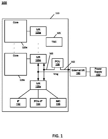
FIG. 1 is a block diagram of a portion of a system in accordance with an embodiment of the present invention.
FIG. 2 is a block diagram of a processor in accordance with an embodiment of the present invention.
FIG. 3 is a block diagram of a multi-domain processor in accordance with another embodiment of the present invention.
FIG. 4 is an embodiment of a processor including multiple cores.
FIG. 5 is a block diagram of a micro-architecture of a processor core in accordance with one embodiment of the present invention.
FIG. 6 is a block diagram of a micro-architecture of a processor core in accordance with another embodiment.
FIG. 7 is a block diagram of a micro-architecture of a processor core in accordance with yet another embodiment.
FIG. 8 is a block diagram of a micro-architecture of a processor core in accordance with a still further embodiment.
FIG. 9 is a block diagram of a processor in accordance with another embodiment of the present invention.
FIG. 10 is a block diagram of a representative SoC in accordance with an embodiment of the present invention.
FIG. 11 is a block diagram of another example SoC in accordance with an embodiment of the present invention.
FIG. 12 is a block diagram of an example system with which embodiments can be used.
FIG. 13 is a block diagram of another example system with which embodiments may be used.
FIG. 14 is a block diagram of a representative computer system.
FIG. 15 is a block diagram of a system in accordance with an embodiment of the present invention.
FIG. 16 is a block diagram of a power control logic in accordance with an embodiment of the present invention.
FIG. 17 is a block diagram of a processor including a hardware power control logic in accordance with another embodiment of the present invention.
FIG. 18 is a flow diagram of a method for controlling power consumption of a processor in accordance with an embodiment of the present invention.
FIG. 19 is a flow diagram of a method for controlling power consumption of a processor in accordance with another embodiment of the present invention.
FIG. 20 is a flow diagram of a method for updating trained model parameters in accordance with an embodiment of the present invention.
In various embodiments, an intelligent multi-core power management controller for a processor is provided that learns workload characteristics on-the-fly and dynamically adjusts power configurations to provide optimal performance per energy. In one embodiment, such power configurations include the number of active cores and threads, as well as an optimal voltage and frequency for each active core. In various embodiments, a machine learning-based performance and energy model identifies particular workload behaviors such as intensive memory accesses and predicts optimal power control, including placing one or more cores into an idle or low power state while saturating memory resources.
In an embodiment, a power management controller is configured with a policy that determines an optimal power configuration and a mechanism to apply the decided configuration to the underlying system. Such policies may include heuristics developed by experts, and/or offline/online machine learning schemes, and may further include a number of user-level and operating system (OS)-level core-to-thread management mechanisms.
A power management controller as described herein may be configured to allocate only needed resources to a workload, so that performance and energy efficiency can be maximized. As an example, memory bound workloads saturate memory resources (such as bandwidth or queues) before all compute resources are fully utilized. If such workloads are executed with all threads and cores active, poor efficiency will result. Some compute bound workloads also suffer from compromised scalability due to various reasons such as increased synchronization overhead. Embodiments apply to equally to other workloads that create slack in a core, such that the core becomes underutilized. Other example workloads include I/O or network bounded workloads. Embodiments may thus identify a best power configuration for different workloads. For example, particular workloads may be identified and underutilized resources for the workloads can be powered off or operate at reduced consumption levels to enable significant energy savings without adversely affecting performance.
In an embodiment, the best power configuration for a workload defines the optimal number of threads and cores, execution units, voltages and frequencies, and so forth. This power configuration depends on many parameters, including both runtime workload behaviors and system power status. In addition, when considering the overheads incurred during transitions between power states, the selection process becomes even more complex. A single, fixed control policy is hard to adapt to various workloads and different systems. Embodiments thus provide a set of different models to evaluate, and an intelligent selector chooses from the identified models. This enables multiple control policies and a flexible selection at runtime. Thus embodiments may be used to determine an optimal power configuration (e.g., number of cores/threads, and voltage/frequency) concurrently for each workload, rather than a predefined control policy based on a single performance/energy prediction model.
Embodiments operate to save energy without adversely affecting performance for memory-intensive workloads, which saturate memory resources before fully utilizing compute resources, which can waste energy in a multicore processor. Embodiments may identify such behaviors and turn off underutilized cores to provide energy savings without a performance sacrifice.
In some embodiments, a heterogeneous multiprocessor may include two different types of cores: one core type optimized for computation and another core type optimized for memory accesses. In one example, both types of cores implement the same instruction set architecture (ISA) but have different microarchitectures, which may facilitate thread migration between the core types.
Compute and memory bounded phases of a program may have very different processor requirements that cannot be optimized by a single core type. For example, a homogeneous multiprocessor optimized for compute workloads may target for a highest core count running at a frequency that can sustain one fused multiply add (FMA) per cycle per core. However, this multiprocessor may not be very energy efficient during a program phase that is mostly waiting for memory return. This is so, as during memory bounded phases, the cores are mostly idle waiting for memory accesses, yet the idle time may not be long enough to warrant placing the core into a low power state. As a result, the idling core at a high frequency can consume unnecessary power.
As such, embodiments provide a heterogeneous multiprocessor that includes two or more specialized core types that are optimized for different operating points. In the examples described herein, two core types, a compute-optimized core (also referred to as a compute-biased core) and a memory-optimized core (also referred to as a memory-biased core) are provided. However understand the scope of the present invention is not limited to 2 core types, and in other cases additional core types optimized for other workload types may be present.
Although the following embodiments are described with reference to energy conservation and energy efficiency in specific integrated circuits, such as in computing platforms or processors, other embodiments are applicable to other types of integrated circuits and logic devices. Similar techniques and teachings of embodiments described herein may be applied to other types of circuits or semiconductor devices that may also benefit from better energy efficiency and energy conservation. For example, the disclosed embodiments are not limited to any particular type of computer systems. That is, disclosed embodiments can be used in many different system types, ranging from server computers (e.g., tower, rack, blade, micro-server and so forth), communications systems, storage systems, desktop computers of any configuration, laptop, notebook, and tablet computers (including 2:1 tablets, phablets and so forth), and may be also used in other devices, such as handheld devices, systems on chip (SoCs), and embedded applications. Some examples of handheld devices include cellular phones such as smartphones, Internet protocol devices, digital cameras, personal digital assistants (PDAs), and handheld PCs. Embedded applications may typically include a microcontroller, a digital signal processor (DSP), network computers (NetPC), set-top boxes, network hubs, wide area network (WAN) switches, wearable devices, or any other system that can perform the functions and operations taught below. More so, embodiments may be implemented in mobile terminals having standard voice functionality such as mobile phones, smartphones and phablets, and/or in non-mobile terminals without a standard wireless voice function communication capability, such as many wearables, tablets, notebooks, desktops, micro-servers, servers and so forth. Moreover, the apparatuses, methods, and systems described herein are not limited to physical computing devices, but may also relate to software optimizations for energy conservation and efficiency. As will become readily apparent in the description below, the embodiments of methods, apparatuses, and systems described herein (whether in reference to hardware, firmware, software, or a combination thereof) are vital to a ‘green technology’ future, such as for power conservation and energy efficiency in products that encompass a large portion of the US economy.
Referring now to FIG. 1 , shown is a block diagram of a portion of a system in accordance with an embodiment of the present invention. As shown in FIG. 1 , system 100 may include various components, including a processor 110 which as shown is a multicore processor. Processor 110 may be coupled to a power supply 150 via an external voltage regulator 160 , which may perform a first voltage conversion to provide a primary regulated voltage to processor 110 .
As seen, processor 110 may be a single die processor including multiple cores 120 .sub.a- 120 .sub.n. In addition, each core may be associated with an integrated voltage regulator (IVR) 125 .sub.a- 125 .sub.n which receives the primary regulated voltage and generates an operating voltage to be provided to one or more agents of the processor associated with the IVR. Accordingly, an IVR implementation may be provided to allow for fine-grained control of voltage and thus power and performance of each individual core. As such, each core can operate at an independent voltage and frequency, enabling great flexibility and affording wide opportunities for balancing power consumption with performance. In some embodiments, the use of multiple IVRs enables the grouping of components into separate power planes, such that power is regulated and supplied by the IVR to only those components in the group. During power management, a given power plane of one IVR may be powered down or off when the processor is placed into a certain low power state, while another power plane of another IVR remains active, or fully powered.
Still referring to FIG. 1 , additional components may be present within the processor including an input/output interface 132 , another interface 134 , and an integrated memory controller 136 . As seen, each of these components may be powered by another integrated voltage regulator 125 .sub.x. In one embodiment, interface 132 may be enable operation for an Intel® Quick Path Interconnect (QPI) interconnect, which provides for point-to-point (PtP) links in a cache coherent protocol that includes multiple layers including a physical layer, a link layer and a protocol layer. In turn, interface 134 may communicate via a Peripheral Component Interconnect Express (PCIe™) protocol.
Also shown is a power control unit (PCU) 138 , which may include hardware, software and/or firmware to perform power management operations with regard to processor 110 . As seen, PCU 138 provides control information to external voltage regulator 160 via a digital interface to cause the voltage regulator to generate the appropriate regulated voltage. PCU 138 also provides control information to IVRs 125 via another digital interface to control the operating voltage generated (or to cause a corresponding IVR to be disabled in a low power mode). In various embodiments, PCU 138 may include a variety of power management logic units to perform hardware-based power management. Such power management may be wholly processor controlled (e.g., by various processor hardware, and which may be triggered by workload and/or power, thermal or other processor constraints) and/or the power management may be performed responsive to external sources (such as a platform or management power management source or system software). As described further herein, PCU 138 may include control logic to perform a workload classification based on a type of workload being executed, and cause the workload to be executed on a potentially different number of cores (and at potentially different performance states) based at least in part on the workload type.
While not shown for ease of illustration, understand that additional components may be present within processor 110 such as uncore logic, and other components such as internal memories, e.g., one or more levels of a cache memory hierarchy and so forth. Furthermore, while shown in the implementation of FIG. 1 with an integrated voltage regulator, embodiments are not so limited.
Note that the power management techniques described herein may be independent of and complementary to an operating system (OS)-based power management (OSPM) mechanism. According to one example OSPM technique, a processor can operate at various performance states or levels, so-called P-states, namely from P 0 to PN. In general, the P 1 performance state may correspond to the highest guaranteed performance state that can be requested by an OS. In addition to this P 1 state, the OS can further request a higher performance state, namely a P 0 state. This P 0 state may thus be an opportunistic or turbo mode state in which, when power and/or thermal budget is available, processor hardware can configure the processor or at least portions thereof to operate at a higher than guaranteed frequency. In many implementations a processor can include multiple so-called bin frequencies above the P 1 guaranteed maximum frequency, exceeding to a maximum peak frequency of the particular processor, as fused or otherwise written into the processor during manufacture. In addition, according to one OSPM mechanism, a processor can operate at various power states or levels. With regard to power states, an OSPM mechanism may specify different power consumption states, generally referred to as C-states, C 0 , C 1 to Cn states. When a core is active, it runs at a C 0 state, and when the core is idle it may be placed in a core low power state, also called a core non-zero C-state (e.g., C 1 -C 6 states), with each C-state being at a lower power consumption level (such that C 6 is a deeper low power state than C 1 , and so forth).
Understand that many different types of power management techniques may be used individually or in combination in different embodiments. As representative examples, a power controller may control the processor to be power managed by some form of dynamic voltage frequency scaling (DVFS) in which an operating voltage and/or operating frequency of one or more cores or other processor logic may be dynamically controlled to reduce power consumption in certain situations. In an example, DVFS may be performed using Enhanced Intel SpeedStep™ technology available from Intel Corporation, Santa Clara, Calif., to provide optimal performance at a lowest power consumption level. In another example, DVFS may be performed using Intel TurboBoost™ technology to enable one or more cores or other compute engines to operate at a higher than guaranteed operating frequency based on conditions (e.g., workload and availability).
Another power management technique that may be used in certain examples is dynamic swapping of workloads between different compute engines. For example, the processor may include asymmetric cores or other processing engines that operate at different power consumption levels, such that in a power constrained situation, one or more workloads can be dynamically switched to execute on a lower power core or other compute engine. Another exemplary power management technique is hardware duty cycling (HDC), which may cause cores and/or other compute engines to be periodically enabled and disabled according to a duty cycle, such that one or more cores may be made inactive during an inactive period of the duty cycle and made active during an active period of the duty cycle. Although described with these particular examples, understand that many other power management techniques may be used in particular embodiments.
Embodiments can be implemented in processors for various markets including server processors, desktop processors, mobile processors and so forth. Referring now to FIG. 2 , shown is a block diagram of a processor in accordance with an embodiment of the present invention. As shown in FIG. 2 , processor 200 may be a multicore processor including a plurality of cores 210 .sub.a- 210 .sub.n. In one embodiment, each such core may be of an independent power domain and can be configured to enter and exit active states and/or maximum performance states based on workload. The various cores may be coupled via an interconnect 215 to a system agent or uncore 220 that includes various components. As seen, the uncore 220 may include a shared cache 230 which may be a last level cache. In addition, the uncore may include an integrated memory controller 240 to communicate with a system memory (not shown in FIG. 2 ), e.g., via a memory bus. Uncore 220 also includes various interfaces 250 and a power control unit 255 , which may include a workload classification logic 256 (that may include or be associated with machine learning logic) to classify a workload being executed and perform dynamic control of a number of cores and/or performance state based at least in part thereon, as described herein.
In addition, by interfaces 250 a - 250 n , connection can be made to various off-chip components such as peripheral devices, mass storage and so forth. While shown with this particular implementation in the embodiment of FIG. 2 , the scope of the present invention is not limited in this regard.
Referring now to FIG. 3 , shown is a block diagram of a multi-domain processor in accordance with another embodiment of the present invention. As shown in the embodiment of FIG. 3 , processor 300 includes multiple domains. Specifically, a core domain 310 can include a plurality of cores 310 .sub.0- 310 .sub.n, a graphics domain 320 can include one or more graphics engines, and a system agent domain 350 may further be present. In some embodiments, system agent domain 350 may execute at an independent frequency than the core domain and may remain powered on at all times to handle power control events and power management such that domains 310 and 320 can be controlled to dynamically enter into and exit high power and low power states. Each of domains 310 and 320 may operate at different voltage and/or power. Note that while only shown with three domains, understand the scope of the present invention is not limited in this regard and additional domains can be present in other embodiments. For example, multiple core domains may be present each including at least one core.
In general, each core 310 may further include low level caches in addition to various execution units and additional processing elements. In turn, the various cores may be coupled to each other and to a shared cache memory formed of a plurality of units of a last level cache (LLC) 340 .sub.0- 340 .sub.n. In various embodiments, LLC 340 may be shared amongst the cores and the graphics engine, as well as various media processing circuitry. As seen, a ring interconnect 330 thus couples the cores together, and provides interconnection between the cores, graphics domain 320 and system agent circuitry 350 . In one embodiment, interconnect 330 can be part of the core domain. However in other embodiments the ring interconnect can be of its own domain.
As further seen, system agent domain 350 may include display controller 352 which may provide control of and an interface to an associated display. As further seen, system agent domain 350 may include a power control unit 355 which can include a workload classification logic 356 (itself including machine learning logic) to perform the workload classification-based thread migration and power control techniques as described herein.
As further seen in FIG. 3 , processor 300 can further include an integrated memory controller (IMC) 370 that can provide for an interface to a system memory, such as a dynamic random access memory (DRAM). Multiple interfaces 380 .sub.0- 380 .sub.n may be present to enable interconnection between the processor and other circuitry. For example, in one embodiment at least one direct media interface (DMI) interface may be provided as well as one or more PCIe™ interfaces. Still further, to provide for communications between other agents such as additional processors or other circuitry, one or more QPI interfaces may also be provided. Although shown at this high level in the embodiment of FIG. 3 , understand the scope of the present invention is not limited in this regard.
Referring to FIG. 4 , an embodiment of a processor including multiple cores is illustrated. Processor 400 includes any processor or processing device, such as a microprocessor, an embedded processor, a digital signal processor (DSP), a network processor, a handheld processor, an application processor, a co-processor, a system on a chip (SoC), or other device to execute code. Processor 400 , in one embodiment, includes at least two cores—cores 401 and 402 , which may include asymmetric cores or symmetric cores (the illustrated embodiment). However, processor 400 may include any number of processing elements that may be symmetric or asymmetric.
In one embodiment, a processing element refers to hardware or logic to support a software thread. Examples of hardware processing elements include: a thread unit, a thread slot, a thread, a process unit, a context, a context unit, a logical processor, a hardware thread, a core, and/or any other element, which is capable of holding a state for a processor, such as an execution state or architectural state. In other words, a processing element, in one embodiment, refers to any hardware capable of being independently associated with code, such as a software thread, operating system, application, or other code. A physical processor typically refers to an integrated circuit, which potentially includes any number of other processing elements, such as cores or hardware threads.
A core often refers to logic located on an integrated circuit capable of maintaining an independent architectural state, wherein each independently maintained architectural state is associated with at least some dedicated execution resources. In contrast to cores, a hardware thread typically refers to any logic located on an integrated circuit capable of maintaining an independent architectural state, wherein the independently maintained architectural states share access to execution resources. As can be seen, when certain resources are shared and others are dedicated to an architectural state, the line between the nomenclature of a hardware thread and core overlaps. Yet often, a core and a hardware thread are viewed by an operating system as individual logical processors, where the operating system is able to individually schedule operations on each logical processor.
Physical processor 400 , as illustrated in FIG. 4 , includes two cores, cores 401 and 402 . Here, cores 401 and 402 are considered symmetric cores, i.e., cores with the same configurations, functional units, and/or logic. In another embodiment, core 401 includes an out-of-order processor core, while core 402 includes an in-order processor core. However, cores 401 and 402 may be individually selected from any type of core, such as a native core, a software managed core, a core adapted to execute a native instruction set architecture (ISA), a core adapted to execute a translated ISA, a co-designed core, or other known core. Yet to further the discussion, the functional units illustrated in core 401 are described in further detail below, as the units in core 402 operate in a similar manner.
As depicted, core 401 includes two hardware threads 401 a and 401 b , which may also be referred to as hardware thread slots 401 a and 401 b . Therefore, software entities, such as an operating system, in one embodiment potentially view processor 400 as four separate processors, i.e., four logical processors or processing elements capable of executing four software threads concurrently. As alluded to above, a first thread is associated with architecture state registers 401 a , a second thread is associated with architecture state registers 401 b , a third thread may be associated with architecture state registers 402 a , and a fourth thread may be associated with architecture state registers 402 b . Here, each of the architecture state registers ( 401 a , 401 b , 402 a , and 402 b ) may be referred to as processing elements, thread slots, or thread units, as described above. As illustrated, architecture state registers 401 a are replicated in architecture state registers 401 b , so individual architecture states/contexts are capable of being stored for logical processor 401 a and logical processor 401 b . In core 401 , other smaller resources, such as instruction pointers and renaming logic in allocator and renamer block 430 may also be replicated for threads 401 a and 401 b . Some resources, such as re-order buffers in reorder/retirement unit 435 , ILTB 420 , load/store buffers, and queues may be shared through partitioning. Other resources, such as general purpose internal registers, page-table base register(s), low-level data-cache and data-TLB 415 , execution unit(s) 440 , and portions of out-of-order unit 435 are potentially fully shared.
Processor 400 often includes other resources, which may be fully shared, shared through partitioning, or dedicated by/to processing elements. In FIG. 4 , an embodiment of a purely exemplary processor with illustrative logical units/resources of a processor is illustrated. Note that a processor may include, or omit, any of these functional units, as well as include any other known functional units, logic, or firmware not depicted. As illustrated, core 401 includes a simplified, representative out-of-order (OOO) processor core. But an in-order processor may be utilized in different embodiments. The OOO core includes a branch target buffer 420 to predict branches to be executed/taken and an instruction-translation buffer (I-TLB) 420 to store address translation entries for instructions.
Core 401 further includes decode module 425 coupled to fetch unit 420 to decode fetched elements. Fetch logic, in one embodiment, includes individual sequencers associated with thread slots 401 a , 401 b , respectively. Usually core 401 is associated with a first ISA, which defines/specifies instructions executable on processor 400 . Often machine code instructions that are part of the first ISA include a portion of the instruction (referred to as an opcode), which references/specifies an instruction or operation to be performed. Decode logic 425 includes circuitry that recognizes these instructions from their opcodes and passes the decoded instructions on in the pipeline for processing as defined by the first ISA. For example, decoders 425 , in one embodiment, include logic designed or adapted to recognize specific instructions, such as transactional instruction. As a result of the recognition by decoders 425 , the architecture or core 401 takes specific, predefined actions to perform tasks associated with the appropriate instruction. It is important to note that any of the tasks, blocks, operations, and methods described herein may be performed in response to a single or multiple instructions; some of which may be new or old instructions.
In one example, allocator and renamer block 430 includes an allocator to reserve resources, such as register files to store instruction processing results. However, threads 401 a and 401 b are potentially capable of out-of-order execution, where allocator and renamer block 430 also reserves other resources, such as reorder buffers to track instruction results. Unit 430 may also include a register renamer to rename program/instruction reference registers to other registers internal to processor 400 . Reorder/retirement unit 435 includes components, such as the reorder buffers mentioned above, load buffers, and store buffers, to support out-of-order execution and later in-order retirement of instructions executed out-of-order.
Scheduler and execution unit(s) block 440 , in one embodiment, includes a scheduler unit to schedule instructions/operation on execution units. For example, a floating point instruction is scheduled on a port of an execution unit that has an available floating point execution unit. Register files associated with the execution units are also included to store information instruction processing results. Exemplary execution units include a floating point execution unit, an integer execution unit, a jump execution unit, a load execution unit, a store execution unit, and other known execution units.
Lower level data cache and data translation buffer (D-TLB) 450 are coupled to execution unit(s) 440 . The data cache is to store recently used/operated on elements, such as data operands, which are potentially held in memory coherency states. The D-TLB is to store recent virtual/linear to physical address translations. As a specific example, a processor may include a page table structure to break physical memory into a plurality of virtual pages.
Here, cores 401 and 402 share access to higher-level or further-out cache 410 , which is to cache recently fetched elements. Note that higher-level or further-out refers to cache levels increasing or getting further away from the execution unit(s). In one embodiment, higher-level cache 410 is a last-level data cache—last cache in the memory hierarchy on processor 400 —such as a second or third level data cache. However, higher level cache 410 is not so limited, as it may be associated with or includes an instruction cache. A trace cache—a type of instruction cache—instead may be coupled after decoder 425 to store recently decoded traces.
In the depicted configuration, processor 400 also includes bus interface module 405 and a power controller 460 , which may perform power management in accordance with an embodiment of the present invention. In this scenario, bus interface 405 is to communicate with devices external to processor 400 , such as system memory and other components.
A memory controller 470 may interface with other devices such as one or many memories. In an example, bus interface 405 includes a ring interconnect with a memory controller for interfacing with a memory and a graphics controller for interfacing with a graphics processor. In an SoC environment, even more devices, such as a network interface, coprocessors, memory, graphics processor, and any other known computer devices/interface may be integrated on a single die or integrated circuit to provide small form factor with high functionality and low power consumption.
Referring now to FIG. 5 , shown is a block diagram of a micro-architecture of a processor core in accordance with one embodiment of the present invention. As shown in FIG. 5 , processor core 500 may be a multi-stage pipelined out-of-order processor. Core 500 may operate at various voltages based on a received operating voltage, which may be received from an integrated voltage regulator or external voltage regulator.
As seen in FIG. 5 , core 500 includes front end units 510 , which may be used to fetch instructions to be executed and prepare them for use later in the processor pipeline. For example, front end units 510 may include a fetch unit 501 , an instruction cache 503 , and an instruction decoder 505 . In some implementations, front end units 510 may further include a trace cache, along with microcode storage as well as a micro-operation storage. Fetch unit 501 may fetch macro-instructions, e.g., from memory or instruction cache 503 , and feed them to instruction decoder 505 to decode them into primitives, i.e., micro-operations for execution by the processor.
Coupled between front end units 510 and execution units 520 is an out-of-order (OOO) engine 515 that may be used to receive the micro-instructions and prepare them for execution. More specifically OOO engine 515 may include various buffers to re-order micro-instruction flow and allocate various resources needed for execution, as well as to provide renaming of logical registers onto storage locations within various register files such as register file 530 and extended register file 535 . Register file 530 may include separate register files for integer and floating point operations. For purposes of configuration, control, and additional operations, a set of machine specific registers (MSRs) 538 may also be present and accessible to various logic within core 500 (and external to the core). For example, power limit information may be stored in one or more MSR and be dynamically updated as described herein.
Various resources may be present in execution units 520 , including, for example, various integer, floating point, and single instruction multiple data (SIMD) logic units, among other specialized hardware. For example, such execution units may include one or more arithmetic logic units (ALUs) 522 and one or more vector execution units 524 , among other such execution units.
Results from the execution units may be provided to retirement logic, namely a reorder buffer (ROB) 540 . More specifically, ROB 540 may include various arrays and logic to receive information associated with instructions that are executed. This information is then examined by ROB 540 to determine whether the instructions can be validly retired and result data committed to the architectural state of the processor, or whether one or more exceptions occurred that prevent a proper retirement of the instructions. Of course, ROB 540 may handle other operations associated with retirement.
As shown in FIG. 5 , ROB 540 is coupled to a cache 550 which, in one embodiment may be a low level cache (e.g., an L1 cache) although the scope of the present invention is not limited in this regard. Also, execution units 520 can be directly coupled to cache 550 . From cache 550 , data communication may occur with higher level caches, system memory and so forth. While shown with this high level in the embodiment of FIG. 5 , understand the scope of the present invention is not limited in this regard. For example, while the implementation of FIG. 5 is with regard to an out-of-order machine such as of an Intel® x86 instruction set architecture (ISA), the scope of the present invention is not limited in this regard. That is, other embodiments may be implemented in an in-order processor, a reduced instruction set computing (RISC) processor such as an ARM-based processor, or a processor of another type of ISA that can emulate instructions and operations of a different ISA via an emulation engine and associated logic circuitry.
Referring now to FIG. 6 , shown is a block diagram of a micro-architecture of a processor core in accordance with another embodiment. In the embodiment of FIG. 6 , core 600 may be a low power core of a different micro-architecture, such as an Intel® Atom™-based processor having a relatively limited pipeline depth designed to reduce power consumption. As seen, core 600 includes an instruction cache 610 coupled to provide instructions to an instruction decoder 615 . A branch predictor 605 may be coupled to instruction cache 610 . Note that instruction cache 610 may further be coupled to another level of a cache memory, such as an L2 cache (not shown for ease of illustration in FIG. 6 ). In turn, instruction decoder 615 provides decoded instructions to an issue queue 620 for storage and delivery to a given execution pipeline. A microcode ROM 618 is coupled to instruction decoder 615 .
A floating point pipeline 630 includes a floating point register file 632 which may include a plurality of architectural registers of a given bit with such as 128, 256 or 512 bits. Pipeline 630 includes a floating point scheduler 634 to schedule instructions for execution on one of multiple execution units of the pipeline. In the embodiment shown, such execution units include an ALU 635 , a shuffle unit 636 , and a floating point adder 638 . In turn, results generated in these execution units may be provided back to buffers and/or registers of register file 632 . Of course understand while shown with these few example execution units, additional or different floating point execution units may be present in another embodiment.
An integer pipeline 640 also may be provided. In the embodiment shown, pipeline 640 includes an integer register file 642 which may include a plurality of architectural registers of a given bit with such as 128 or 256 bits. Pipeline 640 includes an integer scheduler 644 to schedule instructions for execution on one of multiple execution units of the pipeline. In the embodiment shown, such execution units include an ALU 645 , a shifter unit 646 , and a jump execution unit 648 . In turn, results generated in these execution units may be provided back to buffers and/or registers of register file 642 . Of course understand while shown with these few example execution units, additional or different integer execution units may be present in another embodiment.
The description continues in the full USPTO document.
About 6,296 words. The USPTO PDF has it with every drawing.
Fees are due 3.5, 7.5 and 11.5 years after grant. This patent expired on March 6, 2026, so the fee marked "not paid" was the one that went unpaid.
PERFORMING POWER MANAGEMENT IN A MULTICORE PROCESSOR
Filed Feb 2015 · published Aug 2016Performing power management in a multicore processor
Filed Feb 2015 · granted Mar 2018Earlier publications, parents and continuations. None of them can still be enforced, or this patent would not be listed.
Prior art cited by the examiner or applicant. Useful when you check your own idea for novelty.
Everything on this page comes from the documents linked above.