Cross references to related applications
The present application is a national stage of International Application No. PCT/JP2012/072331 filed on Sep. 3, 2012 and claims priority to P.R.C Patent Application No. 201110281329.6 filed in the State Intellectual Property Office of The People's Republic of China on Sep. 21, 2011, the disclosure of which is incorporated herein by reference.
Background
The present disclosure relates to a multi-junction (also called a tandem-type, a stack-type, or a lamination-type) solar cell, a photoelectric conversion device, and a compound-semiconductor-layer lamination structure that use a compound semiconductor.
As a compound semiconductor configured of two or more types of elements, many types exist depending on a combination of the elements. Also, by laminating a lot of compound semiconductor layers made of different materials, a compound semiconductor device having various functions and various physical properties are achievable. As an example thereof, a solar cell may be mentioned. Here, as a solar cell, a silicon-based solar cell that uses silicon as a semiconductor, a compound semiconductor solar cell that uses a compound semiconductor, an organic solar cell that uses an organic material, etc. may be mentioned. In particular, the compound semiconductor solar cell has been developed aiming further improvement in energy conversion efficiency.
As a means for improving energy conversion efficiency of the compound semiconductor solar cell, there are provided a method in which a plurality of sub-cells each configured of a thin-film solar cell that is configured of a plurality of compound semiconductor layers are laminated to form a multi-junction solar cell, a method in which an effective combination of compound semiconductor materials configuring the compound semiconductor layers are searched, etc. Each of compound semiconductors such as GaAs and InP has a unique band gap, and a wavelength of light to be absorbed is different depending on this difference in band gap. Therefore, by laminating a plurality of types of sub-cells, efficiency of absorption of solar light that has a wide wavelength range is improved. In lamination, a combination of lattice constants and physical property values (such as band gaps) of crystal structures of the compound semiconductors configuring the respective sub-cells is important.
By the way, most of the multi-junction solar cells under current consideration are classified into a lattice-matched type and a lattice-mismatched type. In the lattice-matched type, compound semiconductor layers are laminated that are made of compound semiconductors having lattice constants that are almost the same with one another. In the lattice-mismatched type, compound semiconductor layers are laminated that are made of compound semiconductors having lattice constants that are different from one another with the use of metamorphic growth accompanied by dislocation. However, in the metamorphic growth method, undesirable lattice mismatch inevitably occurs, and therefore, there is an issue that quality of the compound semiconductors is significantly lowered.
On the other hand, in recent years, there has been proposed a method of manufacturing a multi-junction solar cell that utilizes a substrate bonding technique in junction of compound semiconductor layers, and a four-junction solar cell that has a structure of In.sub.0.48Ga.sub.0.52P/GaAs/InGaAsP/In.sub.0.53Ga.sub.0.47As has been reported.
This substrate bonding technique is a technique to form homojunction or heterojunction between the compound semiconductor layers to be joined, and may be classified, for example, into a direct bonding scheme in which different compound semiconductor layers are bonded directly to one another (for example, see Non-patent Literature 1: “Wafer Bonding and Layer Transfer Processes for High Efficiency Solar Cells”, NCPV and Solar Program Review Meeting 2003), and a scheme in which the compound semiconductor layers are joined with a connection layer in between. The substrate bonding technique has an advantage that it is not accompanied by an increase in threading dislocation. Existence of the threading dislocation leads to a not-preferable effect on electron performance of the compound semiconductor layers. In particular, the existence of the threading dislocation provides an easy diffusion path in the compound semiconductor layers as with a dopant and a recombination center, and causes a decrease in carrier density of the compound semiconductor layers. Also, the substrate bonding technique resolves the issue of lattice mismatch, and further avoids epitaxial growth caused by the lattice mismatch. Therefore, threading dislocation density that degrades the performance of the solar cell is largely reduced. In this substrate bonding technique, a covalent bonding is formed in an interface between different substances, in particular, in a hetero interface. At this time, it is important to perform a substrate junction process at a temperature by which thermal variation does not exceed a dynamic barrier necessary for progression in threading dislocation.
In junction by the direct bonding scheme, semiconductor-semiconductor bonding is performed in a nuclear scale. Therefore, transparency, heat conductivity, heat resistance, and reliability of the junction portion are superior than those in a case where junction is formed with the use of metal paste, a glass raw material (frit), etc. In this direct bonding scheme, an integrated-type or two-terminal compound semiconductor device is allowed to be integrated to a module with simplicity equivalent to that in a solar cell configured of a single-junction device, specifically, only by alloying the respective compound semiconductor layers to be laminated. CITATION LIST Non-Patent Literature
Non-patent Literature 1: Wafer Bonding and Layer Transfer Processes for High Efficiency Solar Cells, NCPV and Solar Program Review Meeting 2003 SUMMARY
By the way, in order to improve efficiency in utilizing solar light, it is necessary to take in solar light spectrum in a wide range. A maximum wavelength of the solar light spectrum is 2.5 μm. On the other hand, for example, in the above-described Non-patent Literature 1, the lowermost layer is configured of an InGaAs layer having a band gap of 0.72 eV, and this InGaAs layer is capable of only taking in the solar light having a wavelength of about 1.7 μm. In order to take in the solar light spectrum in a wide range, it is necessary to configure the sub-cell with the use of a compound semiconductor layer that has a further-lower band gap value. However, as long as the present inventors have examined, a technology is not known to provide a sub-cell formed of a compound semiconductor that has a desirable band gap while allowing, as a whole, a lattice constant of a base (for example, a substrate for film formation) for forming such a sub-cell to be matched with a lattice constant of the compound semiconductor that configures the sub-cell.
Therefore, it is desirable to provide a multi-junction solar cell in which lattice match is established, as a whole, with a material configuring the base and that includes a sub-cell formed of a compound semiconductor having a desirable band gap, or a photoelectric conversion device or a compound-semiconductor-layer lamination structure that includes a compound semiconductor layer.
A multi-junction solar cell according to an embodiment of the present disclosure includes a plurality of sub-cells that are laminated, in which light enters from the sub-cell located in an uppermost layer to the sub-cell located in a lowermost layer, and electric power is generated in each of the sub-cells,
each of the sub-cells includes a first compound semiconductor layer and a second compound semiconductor layer that are laminated, the first compound semiconductor layer having a first conductivity type, and the second compound semiconductor layer having a second conductivity type that is different from the first conductivity type,
in at least one predetermined sub-cell of the plurality of sub-cells,
the first compound semiconductor layer is configured of at least one first-compound-semiconductor-layer lamination unit in which a 1-A compound semiconductor layer and a 1-B compound semiconductor layer are laminated,
the second compound semiconductor layer is configured of at least one second-compound-semiconductor-layer lamination unit in which a 2-A compound semiconductor layer and a 2-B compound semiconductor layer are laminated,
a compound semiconductor composition configuring the 1-A compound semiconductor layer and a compound semiconductor composition configuring the 2-A compound semiconductor layer are same compound semiconductor composition A,
a compound semiconductor composition configuring the 1-B compound semiconductor layer and a compound semiconductor composition configuring the 2-B compound semiconductor layer are same compound semiconductor composition B,
the compound semiconductor composition A is determined based on a value of a band gap of the predetermined sub-cell,
the compound semiconductor composition B is determined based on a difference between a base lattice constant of a base used at a time of forming the first and second compound semiconductor layers and a lattice constant of the compound semiconductor composition A,
a thickness of the 1-B compound semiconductor layer is determined based on a difference between the base lattice constant and a lattice constant of the compound semiconductor composition B, and on a thickness of the 1-A compound semiconductor layer,
a thickness of the 2-B compound semiconductor layer is determined based on the difference between the base lattice constant and the lattice constant of the compound semiconductor composition B, and on a thickness of the 2-A compound semiconductor layer,
the thicknesses of the 1-A compound semiconductor layer and the 2-A compound semiconductor layer are smaller than a critical film thickness of the compound semiconductor composition A, and are thicknesses that cause no quantum effect, and
the thicknesses of the 1-B compound semiconductor layer and the 2-B compound semiconductor layer are smaller than a critical film thickness of the compound semiconductor composition B, and are thicknesses that cause no quantum effect.
A photoelectric conversion device according to an embodiment of the present disclosure includes a first compound semiconductor layer and a second compound semiconductor layer that are laminated, the first compound semiconductor layer having a first conductivity type, and the second compound semiconductor layer having a second conductivity type that is different from the first conductivity type,
the first compound semiconductor layer is configured of at least one first-compound-semiconductor-layer lamination unit in which a 1-A compound semiconductor layer and a 1-B compound semiconductor layer are laminated,
the second compound semiconductor layer is configured of at least one second-compound-semiconductor-layer lamination unit in which a 2-A compound semiconductor layer and a 2-B compound semiconductor layer are laminated,
a compound semiconductor composition configuring the 1-A compound semiconductor layer and a compound semiconductor composition configuring the 2-A compound semiconductor layer are same compound semiconductor composition A,
a compound semiconductor composition configuring the 1-B compound semiconductor layer and a compound semiconductor composition configuring the 2-B compound semiconductor layer are same compound semiconductor composition B,
the compound semiconductor composition A is determined based on a value of a band gap of the photoelectric conversion device,
the compound semiconductor composition B is determined based on a difference between a base lattice constant of a base used at a time of forming the first and second compound semiconductor layers and a lattice constant of the compound semiconductor composition A,
a thickness of the 1-B compound semiconductor layer is determined based on a difference between the base lattice constant and a lattice constant of the compound semiconductor composition B, and on a thickness of the 1-A compound semiconductor layer,
a thickness of the 2-B compound semiconductor layer is determined based on the difference between the base lattice constant and the lattice constant of the compound semiconductor composition B, and on a thickness of the 2-A compound semiconductor layer,
the thicknesses of the 1-A compound semiconductor layer and the 2-A compound semiconductor layer are smaller than a critical film thickness of the compound semiconductor composition A, and are thicknesses that cause no quantum effect, and
the thicknesses of the 1-B compound semiconductor layer and the 2-B compound semiconductor layer are smaller than a critical film thickness of the compound semiconductor composition B, and are thicknesses that cause no quantum effect.
A compound-semiconductor-layer lamination structure according to an embodiment of the present disclosure includes at least one compound-semiconductor-layer lamination unit in which an A compound semiconductor layer and a B compound semiconductor layer are laminated,
a compound semiconductor composition B configuring the B compound semiconductor layer is determined based on a difference between a base lattice constant of a base used at a time of forming the A and B compound semiconductor layers and a lattice constant of a compound semiconductor composition A configuring the A compound semiconductor layer,
a thickness of the B compound semiconductor layer is determined based on a difference between the base lattice constant and a lattice constant of the compound semiconductor composition B, and on a thickness of the A compound semiconductor layer,
the thickness of the A compound semiconductor layer is smaller than a critical film thickness of the compound semiconductor composition A, and is a thickness that causes no quantum effect, and
the thicknesses of the B compound semiconductor layer is smaller than a critical film thickness of the compound semiconductor composition B, and is a thickness that causes no quantum effect.
In the predetermined sub-cell in the multi-junction solar cell of an embodiment of the present disclosure, or in the photoelectric conversion device: the first compound semiconductor layer and the second compound semiconductor layer are laminated; the first compound semiconductor layer is configured of at least one first-compound-semiconductor-layer lamination unit in which the 1-A compound semiconductor layer and the 1-B compound semiconductor layer are laminated; and the second compound semiconductor layer is configured of at least one second-compound-semiconductor-layer lamination unit in which the 2-A compound semiconductor layer and the 2-B compound semiconductor layer are laminated. Further, the compound semiconductor composition A that configures the 1-A compound semiconductor layer and the 2-A compound semiconductor layer is determined based on the value of a band gap of the predetermined sub-cell; the compound semiconductor composition B that configures the 1-B compound semiconductor layer and the 2-B compound semiconductor layer is determined based on the difference between the base lattice constant of the base used at the time of forming the first and second compound semiconductor layers and the lattice constant of the compound semiconductor composition A; and the thicknesses of the 1-B compound semiconductor layer and the 2-B compound semiconductor layer are determined based on the difference between the base lattice constant and the lattice constant of the compound semiconductor composition B, and on the thickness of the 1-A compound semiconductor layer and the thickness of the 2-A compound semiconductor layer. Moreover, the thicknesses of the 1-A compound semiconductor layer and the 2-A compound semiconductor layer are smaller than the critical film thickness of the compound semiconductor composition A, and are thicknesses that cause no quantum effect; and the thicknesses of the 1-B compound semiconductor layer and the 2-B compound semiconductor layer are smaller than the critical film thickness of the compound semiconductor composition B, and are thicknesses that cause no quantum effect. In such a manner, a distortion compensation structure is configured of the 1-A compound semiconductor layer and the 1-B compound semiconductor layer.
Further, when a desirable band gap of the predetermined sub-cell, in other words, for example, a wavelength of light which the predetermined sub-cell is allowed to absorb most efficiently is set, or when a desirable band gap of the photoelectric conversion device, in other words, a wavelength of light which the photoelectric conversion device is allowed to absorb most efficiently or a desirable light emission wavelength is set, the compound semiconductor composition A that achieves this is determined. However, usually, the lattice constant of the determined compound semiconductor composition A and the base lattice constant have a difference, in other words, often, lattice-unmatched type is established. Therefore, in order to eliminate this difference, in other words, in order to cancel this difference (in order to establish a lattice-matched type), the compound semiconductor composition B is determined. Moreover, based on the difference between the base lattice constant and the lattice constant of the compound semiconductor composition B, and on the thicknesses of the 1-A compound semiconductor layer and the 2-A compound semiconductor layer, not only the thicknesses of the 1-B compound semiconductor layer and the 2-B compound semiconductor layer are determined, but also, upper-limit values and lower-limit values of layer thicknesses of the 1-A and 2-A compound semiconductor layers and the 1-B and 2-B compound semiconductor layers are defined. In other words, when these layer thicknesses are over the upper-limit values, lattice mismatch is caused, and dislocation may be caused. Further, when these layer thicknesses are smaller than the lower-limit values, the value of the band gap is varied.
In such a manner, in each of the first compound semiconductor layer and the second compound semiconductor layer in the predetermined sub-cell, the compound semiconductor composition is optimized (in other words, the band gap and the lattice constant are optimized), and the layer thickness is optimized. As a result of the above, even when lattice mismatch is established between the 1-A compound semiconductor layer and the base, this lattice mismatch is cancelled by the 1-B compound semiconductor layer, and the first compound semiconductor layer as a whole becomes of a lattice-matched type. The same is applicable also to the second compound semiconductor layer as a whole. Moreover, the first compound semiconductor layer and the second compound semiconductor layer as a whole are allowed to achieve efficient absorption with a desirable wavelength of light or light emission with a desirable wavelength. Further, this may, for example, further improve efficiency in absorption of solar light having a wide wavelength range, in the multi-junction solar cell.
In the compound-semiconductor-layer lamination structure according to an embodiment of the present disclosure: the compound semiconductor composition B is determined based on the difference between the base lattice constant and the lattice constant of the compound semiconductor composition A; and the thickness of the B compound semiconductor layer is determined based on the difference between the base lattice constant and the lattice constant of the compound semiconductor composition B, and on the thickness of the A compound semiconductor layer. Therefore, even when lattice mismatch is established between the A compound semiconductor layer and the base, this lattice mismatch is cancelled by the B compound semiconductor layer, and the compound-semiconductor-layer lamination structure as a whole becomes of a lattice-matched type. Therefore, restriction such as that it is necessary to determine the compound semiconductor composition A being limited by the base lattice constant in order to obtain the lattice-matched type is eased. Therefore, it is possible to expand the range of options for the compound semiconductor composition of the compound semiconductor layer configuring the compound-semiconductor-layer lamination structure, and to improve freedom in options.
Additional features and advantages are described herein, and will be apparent from the following Detailed Description and the figures.
Brief description of the figures
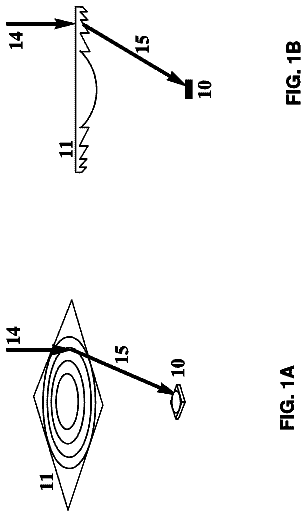
FIG. 1 (A) and (B) of FIG. 1 are a conceptual diagram of a multi-junction solar cell, and a conceptual diagram of a predetermined sub-cell located in a lowermost layer, a photoelectric conversion device, and a compound-semiconductor-layer lamination structure, respectively, in Example 1 or Example 3.
FIG. 2 (A) and (B) of FIG. 2 are conceptual diagrams of a compound semiconductor layer and the like for explaining a method of manufacturing the multi-junction solar cell, the photoelectric conversion device, and the compound-semiconductor-layer lamination structure in Example 3.
FIG. 3 (A) and (B) of FIG. 3 are conceptual diagrams of the compound semiconductor layer and the like for explaining the method of manufacturing the multi-junction solar cell, the photoelectric conversion device, and the compound-semiconductor-layer lamination structure in Example 3, following (B) of FIG. 2 .
FIG. 4 (A) and (B) of FIG. 4 are conceptual diagrams of multi-junction solar cells, photoelectric conversion devices, and compound-semiconductor-layer lamination structures in Example 4 and Example 5, respectively.
FIG. 5 (A) and (B) of FIG. 5 are conceptual diagrams of a compound semiconductor layer and the like for explaining a method of manufacturing a multi-junction solar cell, a photoelectric conversion device, and a compound-semiconductor-layer lamination structure in Example 6.
FIG. 6 (A) and (B) of FIG. 6 are conceptual diagrams of the compound semiconductor layer and the like for explaining the method of manufacturing the multi-junction solar cell, the photoelectric conversion device, and the compound-semiconductor-layer lamination structure in Example 6, following (B) of FIG. 5 .
FIG. 7 is a conceptual diagram of the compound semiconductor layer and the like for explaining the method of manufacturing the multi-junction solar cell, the photoelectric conversion device, and the compound-semiconductor-layer lamination structure in Example 6, following (B) of FIG. 6 .
FIG. 8 (A) and (B) of FIG. 8 are conceptual diagrams of a compound semiconductor layer and the like for explaining a method of manufacturing a multi-junction solar cell, a photoelectric conversion device, and a compound-semiconductor-layer lamination structure in Example 7.
FIG. 9 (A) and (B) of FIG. 9 are conceptual diagrams of the compound semiconductor layer and the like for explaining the method of manufacturing the multi-junction solar cell, the photoelectric conversion device, and the compound-semiconductor-layer lamination structure in Example 7, following (B) of FIG. 8 .
FIG. 10 (A) and (B) of FIG. 10 are conceptual diagrams of the compound semiconductor layer and the like for explaining the method of manufacturing the multi-junction solar cell, the photoelectric conversion device, and the compound-semiconductor-layer lamination structure in Example 7, following (B) of FIG. 9 .
FIG. 11 is a conceptual diagram of a modification of the multi-junction solar cell in Example 1.
FIG. 12 is a graph showing results obtained by variously varying band gaps of a second sub-cell and a first sub-cell, simulating, and determining conversion efficiencies, when a band gap of a fourth sub-cell is 1.910 eV and a band gap of a third sub-cell is 1.420 eV in a multi-junction solar cell in which four sub-cells are laminated.
FIG. 13 is a characteristic diagram illustrating film-forming characteristics of metal atoms.
FIG. 14 is a characteristic diagram illustrating a relationship between a film thickness of a Ti layer and light transmittance.
FIG. 15 (A) and (B) of FIG. 15 are photographs showing a result of an infrared microscopic transmission experiment.
FIG. 16 is a graph showing a relationship between photon energy and an absorption coefficient for each concentration of a p-type dopant in a p-type GaAs layer.
FIG. 17 is a graph showing a relationship between a thickness of the p-type GaAs layer at p-type dopant concentration of 3×10.sup.19 and transmittance of solar light at maximum wavelength of 2.5 μm.
FIG. 18 is a photograph of a bright-field image, of an interface of a junction of an InP substrate and a GaAs substrate, obtained by a scanning transmission electron microscope.
FIG. 19 is a graph showing variation in the film thickness of the Ti layer and the light transmittance over time.
FIG. 20 is a graph showing variation in the film thickness of the Ti layer and the light transmittance over time.
FIG. 21 is a graph showing a result of quantitative analysis of concentration of each atom in each distance in a lamination direction of the multi-junction solar cell in Example 3 based on energy dispersive X-ray spectrometry.
FIG. 22 is a photograph of a cross-section of a bonding junction interface obtained by a transmission electron microscope.
Detailed description
The present disclosure will be described below based on Examples referring to the drawings. However, the present disclosure is not limited to the Examples, and various numerical values, materials, etc. in the Examples are examples. It is to be noted that the description will be given in the following order. 1. Description related to general matters of a multi-junction solar cell, a photoelectric conversion device, and a compound-semiconductor-layer lamination structure of the present disclosure 2. Example 1 (the multi-junction solar cell, the photoelectric conversion device, and the compound-semiconductor-layer lamination structure of the present disclosure) 3. Example 2 (a modification of Example 1) 4. Example 3 (another modification of Example 1) 5. Example 4 (a modification of Example 3) 6. Example 5 (another modification of Example 3) 7. Example 6 (still another modification of Example 3) 8. Example 7 (a modification of Example 6) and others
[Description Related to General Matters of a Multi-junction Solar Cell, a Photoelectric Conversion Device, and a Compound-semiconductor-layer Lamination Structure of the Present Disclosure]
In a multi-junction solar cell of the present disclosure, a form may be adopted in which a predetermined sub-cell is located in a lowermost layer. A lamination order in a plurality of sub-cells is set to be a lamination order by which a band gap of a compound semiconductor configuring the sub-cell becomes larger as the compound semiconductor is closer to a light incident side, that is, a lamination order by which the band gaps of the compound semiconductors are larger in order from a support substrate side to a second electrode side which will be described later. In some cases, part of the plurality of sub-cells may be configured of a Ge layer.
In the multi-junction solar cell of the present disclosure including the above-described preferable form, or the photoelectric conversion device of the present disclosure or the compound-semiconductor-layer lamination structure of the present disclosure, a form may be adopted in which a group of atoms configuring the compound semiconductor composition A is same as a group of atoms configuring the compound semiconductor composition B. Further, in this case, a form may be adopted in which atomic percentage of the group of atoms configuring the compound semiconductor composition A is different from atomic percentage of the group of atoms configuring the compound semiconductor composition B.
Moreover, a value of the band gap of the predetermined sub-cell in the multi-junction solar cell of the present disclosure including the above-described various preferable forms, or a value of the band gap of the photoelectric conversion device in the photoelectric conversion device of the present disclosure including the above-described various preferable forms may be preferably from 0.45 eV to 0.75 eV both inclusive.
Further, in the multi-junction solar cell of the present disclosure including the above-described preferable forms and configurations, or in the photoelectric conversion device of the present disclosure or the compound-semiconductor-layer lamination structure of the present disclosure, a value of a band gap of the compound semiconductor composition B may be desirably larger than a value of a band gap of the compound semiconductor composition A.
Further, in the multi-junction solar cell or the photoelectric conversion device of the present disclosure including the above-described preferable forms and configurations, or in the compound-semiconductor-layer lamination structure of the present disclosure, |( LC .sub.A −LC .sub.0)/ LC .sub.0|≦1×10.sup.−3 and 0.25≦|( LC .sub.B −LC .sub.0)/( LC .sub.A −LC .sub.0)|≦4.0 may be preferably satisfied where LC.sub.A is the lattice constant of the compound semiconductor composition A, LC.sub.B is the lattice constant of the compound semiconductor composition B, and LC.sub.0 is the base lattice constant. Further, in this case, LC .sub.A −LC .sub.0>0 and LC .sub.B −LC .sub.0<0 may be more preferably established.
Further, in the multi-junction solar cell or the photoelectric conversion device of the present disclosure including the above-described preferable forms and configurations, or in the compound-semiconductor-layer lamination structure of the present disclosure, −1×10.sup.−3≦{( t .sub.B .Math.LC .sub.B +t .sub.A .Math.LC .sub.A)/( t .sub.B +t .sub.A)− LC .sub.0 }/LC .sub.0≦1×10.sup.−3 may be desirably satisfied where LC.sub.A is the lattice constant of the compound semiconductor composition A, LC.sub.B is the lattice constant of the compound semiconductor composition B, LC.sub.0 is the base lattice constant, t.sub.A is the thickness of the 1-A compound semiconductor layer and the 2-A compound semiconductor layer (or the thickness of the A compound semiconductor layer), and t.sub.B is the thickness of the 1-B compound semiconductor layer and the 2-B compound semiconductor layer (or the thickness of the B compound semiconductor layer).
Further, in the multi-junction solar cell or the photoelectric conversion device of the present disclosure including the above-described various preferable forms and configurations, or in the compound-semiconductor-layer lamination structure of the present disclosure, a configuration may be adopted in which the base is formed of InP, the compound semiconductor composition A is In.sub.xGa.sub.1-31 xAs, and the compound semiconductor composition B is In.sub.yGa.sub.1−yAs (where x>y). Further, in this case, 0.53≦x≦0.86 and 0≦y≦0.53 may be more preferably established. Alternatively, a configuration may be adopted in which the base is formed of InP, the compound semiconductor composition A is (InP).sub.1−z(In.sub.x′Ga.sub.1−x′As).sub.z, and the compound semiconductor composition B is (InP).sub.1−z(In.sub.y′Ga.sub.1−y′As).sub.z (where x′>y′). Further, in this case, 0.53≦x′≦0.86, 0≦y′≦0.53, and 0<z<1.0 may be more preferably established.
In the multi-junction solar cell or the photoelectric conversion device of the present disclosure including the above-described various preferable forms and configurations, or in the compound-semiconductor-layer lamination structure of the present disclosure (hereinafter, they may be collectively and simply referred to as “present disclosure” in some cases), the thicknesses of the 1-A compound semiconductor layer and the 2-A compound semiconductor layer are smaller than a critical film thickness of the compound semiconductor composition A, the thicknesses of the 1-B compound semiconductor layer and the 2-B compound semiconductor layer are smaller than a critical film thickness of the compound semiconductor composition B, the thickness of the A compound semiconductor layer is smaller than a critical film thickness of the compound semiconductor composition A, and the thicknesses of the B compound semiconductor layer is smaller than a critical film thickness of the compound semiconductor composition B. Here, when the thickness of the compound semiconductor layer is smaller than the critical film thickness, lattice mismatch is reduced due to distortion of crystalline lattice of the compound semiconductor crystal configuring the compound semiconductor layer, and thereby, occurrence of dislocation is suppressed. Further, the thicknesses of the 1-A compound semiconductor layer and the 2-A compound semiconductor layer are thicknesses that cause no quantum effect, the thicknesses of the 1-B compound semiconductor layer and the 2-B compound semiconductor layer are thicknesses that cause no quantum effect, the thickness of the A compound semiconductor layer is a thickness that causes no quantum effect, and the thickness of the B compound semiconductor layer is a thickness that causes no quantum effect. Here, “cause no quantum effect” means that quantum level is not generated even when surrounded by a double hetero barrier when the film thickness is equal to or larger than the de Broglie wave (from several nanometers to 20 nm both inclusive).
When the plurality of sub-cells are laminated in the multi-junction solar cell of the present disclosure, the lattice-mismatch type may be established between the sub-cells in some cases depending on the lattice constants of the compound semiconductors of the compound semiconductor layers configuring the sub-cells. In such a case, the sub-cell and the sub-cell that are to be the lattice-mismatched type may be desirably connected (joined) with the use of an amorphous connection layer formed of an electrically-conductive material. Alternatively, also in a case where the photoelectric conversion device of the present disclosure and a photoelectric conversion device other than that of the present disclosure are laminated, the lattice-mismatched type may be established in some cases depending on lattice constants of the compound semiconductors configuring the adjacent compound semiconductor layers between the laminated photoelectric conversion devices. In such a case, the compound semiconductor layer and the compound semiconductor layer that are to be the lattice-mismatched type may be desirably connected (joined) with the use of an amorphous connection layer formed of an electrically-conductive material. By connecting (joining) with the use of the amorphous connection layer formed of the electrically-conductive material in such a manner, contact resistance of a junction interface of the sub-cells or the compound semiconductor layers is reduced, and energy conversion efficiency is improved. It is to be noted that, in the description below, the multi-junction solar cell or the laminated photoelectric conversion devices provided with such a connection layer may be collectively referred to as “multi-junction solar cell of the present disclosure and the like provided with a connection layer” in some cases.
In the multi-junction solar cell of the present disclosure and the like provided with the connection layer in such a manner, depending on the lattice constants of the compound semiconductors that configure adjacent sub-cells or adjacent compound semiconductor layers, the adjacent sub-cells or the adjacent compound semiconductor layers may be of a lattice-matched type or a lattice-mismatched type. However, in the multi-junction solar cell of the present disclosure and the like provided with the connection layer as a whole, these lattice-matched type/lattice-mismatched type exist in a mixed manner. In the multi-junction solar cell of the present disclosure and the like provided with the connection layer, where a lattice constant of a compound semiconductor that configures one sub-cell or one compound semiconductor layer that is adjacent to the connection layer is Lc.sub.1, and a lattice constant of a compound semiconductor that configures the other sub-cell or the other compound semiconductor layer that is adjacent to the connection layer is Lc.sub.2, being the lattice-mismatched type means, being a type that satisfies: ( Lc .sub.1 −Lc .sub.2)/ Lc .sub.1≧1×10.sup.3 (A) or ( Lc .sub.1 −Lc .sub.2)/ Lc .sub.1≦−1×10.sup.−3 (B). It is to be noted that, when a value of (Lc.sub.1−Lc.sub.2)/Lc.sub.1 is out of the above-described range, that is, when the value satisfies: −1×10.sup.−3<( Lc .sub.1 −Lc .sub.2)/ Lc .sub.1<1×10.sup.−3 (C), it is the lattice-matched type. Further, in the multi-junction solar cell of the present disclosure and the like provided with the connection layer including such a preferable form, it may be preferable to adopt a form in which a tunnel junction layer is provided in a place between the adjacent sub-cells in which the connection layer is not provided. The same is applicable to, or the same may be adopted in the multi-junction solar cell and the photoelectric conversion device of the present disclosure including the above-described various preferable forms and configurations.
Here, as described above, the connection layer is a layer having amorphous characteristics, and is configured of metal or alloy. Specifically, as a material configuring the connection layer, it may be preferable to use a material having ohmic characteristics with respect to the compound semiconductor layer to be connected, more specifically, metal or alloy having a work function that is smaller than a Fermi level of an n-type semiconductor or is larger than a Fermi level of a p-type semiconductor. Accordingly, contact resistance is significantly reduced, and favorable ohmic connection is achievable. It is to be noted that “amorphous connection layer” or “connection layer having amorphous characteristics” means a state that does not have long-term orderly characteristics as in crystal and that does not allow a lattice image to be observed in an image taken by a transmission electron microscope as shown in FIG. 22 .
A metal thin film (having a thickness of several nanometers or smaller, for example) is typically formed based on a PVD method such as a vacuum evaporation method and a sputtering method. However, at that time, the metal thin film is often formed in an island-like shape and is rarely formed in a layer-like shape. Further, when the metal thin film is formed in an island-like shape, it is difficult to control the film thickness with high accuracy. In formation of a metal thin film based on the vacuum evaporation method, often, an island is formed after atoms and molecules absorbed on a base have undergone processes such as surface diffusion, collision and aggregation, and desorption, and the island grows to be combined with an adjacent island, thereby forming a continuous thin film. At that time, formation of an island, transition from being amorphous to being a crystal layer, variation in crystal alignment, etc. occur.
The description continues in the full USPTO document.
 Lapsed, fee not paid11 drawings