Lapsed, fee not paid4 drawings
Cameras, Displays & Optics · US 9,897,833 B2
Array substrate and liquid crystal display panel
The present invention provides an array substrate and a liquid crystal display panel.
US 9,897,848 B2 · Assignee: SHENZHEN CHINA STAR OPTOELECTRONICS TECHNOLOGY CO., LTD. · Inventors: Chen; Lixuan
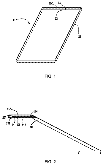
Sheet 1 of 7 from the published document. All sheets in the USPTO PDF
The invention provides a manufacturing method of color resist layer to manufacture the color resist layer by micro transfer printing (MTP), comprising forming a color resist thin film on a first substrate, using a MTP transfer stamp to adsorb a part of the color resist thin film to the plurality of protrusions of the MTP transfer stamp, and transferring the color resist thin film adsorbed by the plurality of protrusions of the MTP transfer stamp to the second substrate to form the color resist layer on the second substrate. The method uses the protrusions of the MTP transfer stamp to form the pattern to control the pattern of the color resist layer instead of exposure and development. No color resist material is wasted, the cost is reduced and the process is simple and widely applicable.
1 of 7 drawing sheets so far from the published document, cropped to the drawing. Every sheet is in the USPTO PDF.
What the patent claimed, word for word. All of it is now free to use.
The present invention relates to the field of display, and in particular to a manufacturing method of color resist layer. 2. The Related Arts
The liquid crystal display (LCD), due to the advantages of high display quality, low power-consumption, thin size, and no radiation, is widely used in mobile phones, TV, PDA, digital camera, notebook PC, desktop PC, and so on.
In general, the LCD panel comprises a color filter (CF) substrate, a thin film transistor (TFT) substrate, an LCD sandwiches between the CF substrate and the TFT substrate, and a sealant; whose manufacturing process comprises an array process (thin film, lithography, etching and stripping), a cell process (attaching TFT substrate and CF substrate), and module assembly process (driver IC and the printed circuit board lamination); wherein the array process is mainly to form TFT substrate, for controlling the LC molecules motion; the cell process is mainly to add LC between the TFT substrate and the CF substrate; and the module assembly process is mainly to laminate the driver IC and integrate the printed circuit board, so as to drive the LC molecules to rotate to generate the images.
The CF substrate is a main part for the LCD. The known manufacturing method for LCD is to manufacture a black matrix (BM) before manufacturing a color resist layer (comprising red color resist, green color resist and blue color resist). The following takes the manufacturing method for res color resist as example to describe the color resist layer manufacturing in known technology: first, coating a red color resist material on the substrate, and then red color resist is cured to become a red color resist thin film, followed by exposure and development processes to form patterned red color resist layer. The drawback is that a large amount of red color resist material is developed and wasted in the above method.
The micro transfer printing is a technology to transfer a micro element grown on a substrate to another substrate by a patterned polydimethylsiloxane (PDMS) transfer stamp to be adsorbed to the micro element off from the substrate, and then the micro element adsorbed by the PDMS transfer stamp is attached to the pre-set position on another substrate, and then the PDMS transfer stamp is lifted off to accomplish micro element transfer.
The object of the present invention is to provide a manufacturing method of color resist layer, able to reduce the color resist material consumption and the manufacturing cost.
To achieve the above object, the present invention provides a manufacturing method of color resist layer, which comprises: Step 1 : providing a first substrate, coating a color resist material on the first substrate, and curing the color resist material to form a color resist thin film; Step 2 : providing a micro transfer printing (MTP) transfer stamp, a surface on one side of the MTP transfer stamp having a plurality of protrusions, the plurality of protrusions forming a pattern matching the pattern of a color resist layer to be formed; Step 3 : using the MTP transfer stamp to adsorb a part of the color resist thin film to the plurality of protrusions of the MTP transfer stamp; Step 4 : providing a second substrate, aligning the MTP transfer stamp and the second substrate, releasing the color resist thin film adsorbed by the plurality of protrusions of the MTP transfer stamp to the second substrate to form the color resist layer on the second substrate.
In Step 1 , the color resist material comprises: red color resist material, green color resist material, blue color resist material or white color resist material.
The MTP transfer stamp is a polydimethylsiloxane (PDMS) transfer stamp.
Specifically, Step 3 comprises: attaching the surface on one side of the MTP transfer stamp having a plurality of protrusions to the color resist thin film, and then peeling the MTP transfer stamp off from the color resist thin film so that a part of the color resist thin film is adsorbed to the plurality of protrusions of the MTP transfer stamp.
Specifically, Step 4 comprises: attaching the surface on one side of the MTP transfer stamp having a plurality of protrusions to the second substrate, and then peeling the MTP transfer stamp off from the second substrate so as to form the color resist layer on the second substrate.
The adhesion strength of the MTP transfer stamp on the color resist thin film is proportional to the speed the MTP transfer stamp peels off.
The second substrate is a glass substrate.
The manufacturing method of the color resist layer is applicable to color-filter-on-array (COA) LCD panel, black-matrix-on array (BOA) LCD panel and white organic light-emitting diode (WOLED) LCD panel.
The present invention also provides a manufacturing method of color resist layer, which comprises: Step 1 : providing a first substrate, coating a color resist material on the first substrate, and curing the color resist material to form a color resist thin film; Step 2 : providing a micro transfer printing (MTP) transfer stamp, a surface on one side of the MTP transfer stamp having a plurality of protrusions, the plurality of protrusions forming a pattern matching the pattern of a color resist layer to be formed; Step 3 : using the MTP transfer stamp to adsorb a part of the color resist thin film to the plurality of protrusions of the MTP transfer stamp; Step 4 : providing a second substrate, aligning the MTP transfer stamp and the second substrate, releasing the color resist thin film adsorbed by the plurality of protrusions of the MTP transfer stamp to the second substrate to form the color resist layer on the second substrate; wherein specifically, Step 3 comprising: attaching the surface on one side of the MTP transfer stamp having a plurality of protrusions to the color resist thin film, and then peeling the MTP transfer stamp off from the color resist thin film so that a part of the color resist thin film being adsorbed to the plurality of protrusions of the MTP transfer stamp; wherein specifically, Step 4 comprising: attaching the surface on one side of the MTP transfer stamp having a plurality of protrusions to the second substrate, and then peeling the MTP transfer stamp off from the second substrate so as to form the color resist layer on the second substrate.
Compared to the known techniques, the present invention provides the following advantages: the present invention provides a manufacturing method of color resist layer to manufacture the color resist layer by micro transfer printing (MTP), comprising forming a color resist thin film on a first substrate, using a MTP transfer stamp to adsorb a part of the color resist thin film to the plurality of protrusions of the MTP transfer stamp, and transferring the color resist thin film adsorbed by the plurality of protrusions of the MTP transfer stamp to the second substrate to form the color resist layer on the second substrate. The method uses the protrusions of the MTP transfer stamp to form the pattern to control the pattern of the color resist layer instead of exposure and development. No color resist material is wasted, the cost is reduced and the process is simple and widely applicable.
To make the technical solution of the embodiments according to the present invention, a brief description of the drawings that are necessary for the illustration of the embodiments will be given as follows. Apparently, the drawings described below show only example embodiments of the present invention and for those having ordinary skills in the art, other drawings may be easily obtained from these drawings without paying any creative effort. In the drawings:
FIG. 1 is a schematic view showing Step 1 of the manufacturing method of color resist layer provided by an embodiment of the present invention;
FIG. 2 is a schematic view showing Step 2 of the manufacturing method of color resist layer provided by an embodiment of the present invention;
FIG. 3 is a schematic view showing Step 3 of the manufacturing method of color resist layer provided by an embodiment of the present invention;
FIG. 4 and FIG. 5 are schematic views showing Step 4 of the manufacturing method of color resist layer provided by an embodiment of the present invention;
FIG. 6 is a schematic view showing the relation between the speed at which the MTP transfer stamp peels off and the adhesion strength of the MTP transfer stamp on the color resist thin film in the manufacturing method of color resist layer provided by an embodiment of the present invention; and
FIG. 7 is a schematic view showing the flowchart of the manufacturing method of color resist layer provided by an embodiment of the present invention.
To further explain the technical means and effect of the present invention, the following refers to embodiments and drawings for detailed description.
Refer to FIG. 7 . The present invention provides a manufacturing method of color resist layer, which comprises:
Step 1 : as shown in FIG. 1 , providing a first substrate 1 , coating a color resist material on the first substrate 1 , and curing the color resist material to form a color resist thin film 2 .
Specifically, the color of the color resist material can be any colors required by the application, such as, red color resist material, green color resist material, blue color resist material or white color resist material.
In Step 1 , the color resist material is distributed in a solution and the solution with distributed color resist material is coated on the first substrate 1 , then a bake process is used to cure the color resist material to form the color resist thin film 2 . The color resist thin film 2 has no pattern and covers entirely over the first substrate.
Step 2 : as shown in FIG. 2 , providing a micro transfer printing (MTP) transfer stamp 3 , a surface on one side of the MTP transfer stamp 3 having a plurality of protrusions 4 , the plurality of protrusions 4 forming a pattern matching the pattern of a color resist layer to be formed.
Optionally, the MTP transfer stamp is a polydimethylsiloxane (PDMS) transfer stamp.
Step 3 : as shown in FIG. 3 , using the MTP transfer stamp 3 to adsorb a part of the color resist thin film 2 to the plurality of protrusions 4 of the MTP transfer stamp 3 .
Specifically, because the pattern formed by the plurality of protrusions 4 is the same as the pattern of the color resist layer to be formed, the pattern of the such color resist film 4 adsorbed on the plurality of protrusions 4 is also the same as the pattern of the color resist layer to be formed.
Moreover, Step 3 specifically comprises: attaching the surface on one side of the MTP transfer stamp 3 having a plurality of protrusions 4 to the color resist thin film 2 , and then peeling the MTP transfer stamp 3 off from the color resist thin film 2 so that a part of the color resist thin film 2 is adsorbed to the plurality of protrusions 4 of the MTP transfer stamp 3 .
It should be noted that, as shown in FIG. 6 , the adhesion strength of the MTP transfer stamp on the color resist thin film is proportional to the speed the MTP transfer stamp peels off.
In other words, the higher the peel off speed of the MTP transfer stamp 3 is from the color resist thin film 2 , the larger the adhesion strength of the MTP transfer stamp 3 on the color resist thin film 2 . Because the adhesion strength of the first substrate 1 on the color resist film 2 remains constant, the peel off speed of the MTP transfer stamp can be controlled to make the adhesion strength of the MTP transfer stamp 3 on the color resist thin film 2 greater than the adhesion strength of the first substrate 1 on the color resist film 2 , resulting in a part of color resist thin film 2 being adsorbed to the plurality of protrusions 4 of the MTP transfer stamp 3 .
Step 4 : as shown in FIG. 4 and FIG. 5 , providing a second substrate 5 , aligning the MTP transfer stamp 3 and the second substrate 5 , releasing the color resist thin film 2 adsorbed by the plurality of protrusions 4 of the MTP transfer stamp 3 to the second substrate 5 to form the color resist layer 6 on the second substrate 5 .
Specifically, the second substrate 5 is preferably a glass substrate. Specifically, Step 4 comprises: attaching the surface on one side of the MTP transfer stamp 3 having a plurality of protrusions 4 to the second substrate 5 , and then peeling the MTP transfer stamp 3 off from the second substrate 5 so as to form the color resist layer 6 on the second substrate 5 .
It should be noted that, as shown in FIG. 6 , because the adhesion strength of the second substrate 5 on the color resist film 2 remains constant, the peel off speed of the MTP transfer stamp 3 can be controlled to make the adhesion strength of the MTP transfer stamp 3 on the color resist thin film 2 less than the adhesion strength of the second substrate 5 on the color resist film 2 , resulting in a part of color resist thin film 2 adsorbed to the plurality of protrusions 4 of the MTP transfer stamp 3 being transferred to the second substrate 5 to form the color resist layer 6 of a preset pattern at the corresponding location.
It should be noted that the above manufacturing method of the color resist layer is not only applicable to the color resist layer in the color filter of the conventional LCD, but also applicable to color-filter-on-array (COA) LCD panel, black-matrix-on array (BOA) LCD panel and white organic light-emitting diode (WOLED) LCD panel. The color resist layer is not only a color resist layer with sequentially arranged red, green and blue color resists, but also with sequentially arranged red, green, blue and white color resists, or sequentially arranged red, green, blue and yellow color resists. Take the color resist layer with sequentially arranged red, green and blue color resists as example. The above manufacturing method can be repeated a plurality of times to manufacture the red, green and blue color resists in sequence to form corresponding color resist layer.
In summary, the present invention provides a manufacturing method of color resist layer to manufacture the color resist layer by micro transfer printing (MTP), comprising forming a color resist thin film on a first substrate, using a MTP transfer stamp to adsorb a part of the color resist thin film to the plurality of protrusions of the MTP transfer stamp, and transferring the color resist thin film adsorbed by the plurality of protrusions of the MTP transfer stamp to the second substrate to form the color resist layer on the second substrate. The method uses the protrusions of the MTP transfer stamp to form the pattern to control the pattern of the color resist layer instead of exposure and development. No color resist material is wasted, the cost is reduced and the process is simple and widely applicable.
It should be noted that in the present disclosure the terms, such as, first, second are only for distinguishing an entity or operation from another entity or operation, and does not imply any specific relation or order between the entities or operations. Also, the terms “comprises”, “include”, and other similar variations, do not exclude the inclusion of other non-listed elements. Without further restrictions, the expression “comprises a . . . ” does not exclude other identical elements from presence besides the listed elements.
Embodiments of the present invention have been described, but not intending to impose any unduly constraint to the appended claims. Any modification of equivalent structure or equivalent process made according to the disclosure and drawings of the present invention, or any application thereof, directly or indirectly, to other related fields of technique, is considered encompassed in the scope of protection defined by the clams of the present invention.
About 2,745 words. The USPTO PDF has it with every drawing.
Fees are due 3.5, 7.5 and 11.5 years after grant. This patent expired on February 20, 2026, so the fee marked "not paid" was the one that went unpaid.
MANUFACTURING METHOD OF COLOR RESIST LAYER
Filed Jun 2016 · published Dec 2017Manufacturing method of color resist layer
Filed Jun 2016 · granted Feb 2018Earlier publications, parents and continuations. None of them can still be enforced, or this patent would not be listed.
Prior art cited by the examiner or applicant. Useful when you check your own idea for novelty.
Everything on this page comes from the documents linked above.