Lapsed, fee not paid3 drawings
Hardware & Electronics · US 9,893,399 B2
Waveguide filter
An embodiment of the present invention discloses a waveguide filter, which includes a first waveguide at an upper layer and a second waveguide at a lower layer.
US 9,893,407 B2 · Assignee: TDK CORPORATION · Inventors: Ootsuka; Noriaki et al.
Sheet 1 of 15 from the published document. All sheets in the USPTO PDF
A directional coupler includes: a main line connecting a first port and a second port; first to third subline sections each of which is formed of a line configured to be electromagnetically coupled to the main line; a first matching section provided between the first subline section and the second subline section; a second matching section provided between the second subline section and the third saline section; and a stack for integrating these components. The stack includes a plurality of dielectric layers and a plurality of conductor layers stacked on each other. Each of the first and second matching sections includes two inductors each formed using one or more of the conductor layers, and a capacitor formed using two or more of the conductor layers.
Directional couplers are used for detecting the levels of transmission/reception signals in transmission/reception circuits of wireless communication apparatuses such as cellular phones and wireless LAN communication apparatuses. A directional coupler configured as follows is known as a conventional directional coupler. The directional coupler has an input port, an output port, a coupling port, a terminal port, a main line, and a subline. One end of the main line is connected to the input port, and the other end of the main line is connected to the output port. One end of the subline is connected to the coupling port, and the other end of the subline is connected to the terminal port. The main line and the subline are configured to be electromagnetically coupled to each other. The terminal port is grounded via a terminator having a resistance of, for example, 50 Ω. The input port receive
1 of 15 drawing sheets so far from the published document, cropped to the drawing. Every sheet is in the USPTO PDF.
What the patent claimed, word for word. All of it is now free to use.
The present invention relates to a wideband capable directional coupler.
Directional couplers are used for detecting the levels of transmission/reception signals in transmission/reception circuits of wireless communication apparatuses such as cellular phones and wireless LAN communication apparatuses.
A directional coupler configured as follows is known as a conventional directional coupler. The directional coupler has an input port, an output port, a coupling port, a terminal port, a main line, and a subline. One end of the main line is connected to the input port, and the other end of the main line is connected to the output port. One end of the subline is connected to the coupling port, and the other end of the subline is connected to the terminal port. The main line and the subline are configured to be electromagnetically coupled to each other. The terminal port is grounded via a terminator having a resistance of, for example, 50 Ω. The input port receives a high frequency signal, and the output port outputs the same. The coupling port outputs a coupling signal having a power that depends on the power of the high frequency signal received at the input port.
Major parameters indicating the characteristics of directional couplers include insertion loss, coupling, isolation, directivity, and return loss at the coupling port. Definitions of these parameters will now be described. First, assume that the input port receives a high frequency signal of power P1. In this case, let P2 be the power of the signal output from the output port, P3 be the power of the signal output from the coupling port, and P4 be the power of the signal output from the terminal port. Assuming that the output port receives a high frequency signal of power P02, let P03 be the power of the signal output from the coupling port. Assuming that the coupling port receives a high frequency signal of power P5, let P6 be the power of the signal reflected at the coupling port. Further, let IL represent insertion loss, C represent coupling, I represent isolation, D represent directivity, and RL represent return loss at the coupling port. These parameters are defined by the following equations. IL= 10 log ( P 2 /P 1) [db] C= 10 log ( P 3 /P 1) [db] I= 10 log ( P 03 /P 02) [dB] D =10 log ( P 4 /P 3) [dB] RL= 10 log ( P 6 /P 5) [dB]
The coupling of the conventional directional coupler increases with increasing frequency of the high frequency signal received at the input port. The conventional directional coupler thus suffers from the problem that the frequency response of the coupling is not flat. Where coupling is denoted as −c (dB), an increase in coupling means a decrease in the value of c.
U.S. Pat. No. 9,077,061 B2 discloses a directional coupler aiming to resolve the aforementioned problem. The directional coupler disclosed therein has a subline divided into a first subline and a second subline. One end of the first subline is connected to the coupling port. One end of the second subline is connected to the terminal port. A phase conversion unit is provided between the other end of the first subline and the other end of the second subline. The phase conversion unit causes a phase shift to be generated in a signal passing therethrough in such a manner that the absolute value of the phase shift monotonically increases within the range from 0 degree to 180 degrees as the frequency increases in a predetermined frequency band. The phase conversion unit is specifically a low-pass filter.
Mobile communication systems conforming to the Long Term Evolution (LTE) standard have become practically used in recent years, and further, practical use of mobile communication systems conforming to the LTE-Advanced standard, which is an evolution of the LTE standard, is under study. Carrier Aggregation (CA) is one of the key technologies of the LTE-Advanced standard. CA uses multiple carriers called component carriers simultaneously to enable wideband transmission.
A mobile communication apparatus operable under CA uses multiple frequency bands simultaneously. Accordingly, such a mobile communication apparatus requires a wideband capable directional coupler, that is, a directional coupler usable for multiple signals in multiple frequency bands.
Directional couplers for use in wireless communication apparatuses are sometimes expected to be bidirectional, that is, to exhibit the same characteristics even when used with the input port and the output port reversed and with the coupling port and the terminal port reversed, as compared with when used without reversing them. Examples of situations requiring bidirectionality include when a directional coupler provided in a transmission circuit for supplying a transmission signal to an antenna is used to detect the level of the transmission signal and also the level of a reflected wave signal resulting from the transmission signal reflected at the antenna. The detection of the level of the reflected wave signal by the directional coupler is for the purpose of adjusting the characteristics of an impedance matching element provided between the transmission circuit and the antenna so as to sufficiently reduce the level of the reflected wave signal. In the aforementioned example, when the directional coupler detects the level of a transmission signal, the transmission signal is received at the input port and output from the output port, and the coupling port outputs a signal having a power that depends on the level of the transmission signal. On the other hand, when the directional coupler detects the level of a reflected wave signal, the reflected wave signal is received at the output port and output from the input port, and the terminal port outputs a signal having a power that depends on the level of the reflected wave signal.
JP 2014-057207A discloses a directional coupler that is wideband capable and bidirectional. In the directional coupler disclosed in JP 2014-057207A, the subline includes a first coupling section having strong coupling to the main line, a second coupling section having weak coupling to the main line and located closer to the coupling port than the first coupling section, a third coupling section having weak coupling to the main line and located closer to the isolation port (terminal port) than the first coupling section, a first non-coupling section not coupled to the main line, extending between the first and second coupling sections and having a length of a quarter or more of a wavelength corresponding to the service frequency band, and a second non-coupling section not coupled to the main line, extending between the first and third coupling sections and having a length of a quarter or more of the wavelength corresponding to the service frequency band.
The directional coupler disclosed in U.S. Pat. No. 9,077,061 B2 has insufficient isolation in a frequency band not lower than the cut-off frequency of the low-pass filter. More specifically, where isolation is denoted as −i (dB), this directional coupler does not exhibit a sufficiently large value of i in a frequency band not lower than the cut-off frequency of the low-pass filter. Thus, this directional coupler does not work in a frequency band not lower than the cut-off frequency of the low-pass filter.
We proceed to explain why the directional coupler disclosed in U.S. Pat. No. 9,077,061 B2 does not exhibit sufficiently large value of i in a frequency band not lower than the cut-off frequency of the low-pass filter. In this directional coupler, there are formed a path connecting the connection point between the first subline and the low-pass filter to the ground via only a first capacitor, and a path connecting the connection point between the second subline and the low-pass filter to the ground via only a second capacitor. Consequently, in a frequency band not lower than the cut-off frequency of the low-pass filter, a high frequency signal going from the first sublime to the low-pass filter mostly flows to the ground via the first capacitor, and a high frequency signal going from the second subline to the low-pass filter mostly flows to the ground via the second capacitor. Thus, in this directional coupler, most part of the high frequency signal fails to pass through the low-pass filter in a frequency band not lower than the cut-off frequency of the low-pass filter.
For the reason described above, the directional coupler disclosed in U.S. Pat. No. 9,077,061 B2 is only usable over a limited frequency band lower than the cut-off frequency of the low-pass filter. Providing a wideband capable directional coupler is thus difficult with the technology described in U.S. Pat. No. 9,077,061 B2.
In the directional coupler disclosed in JP 2014-057207A, the subline includes the first and second non-coupling sections each having a length of a quarter or more of the wavelength corresponding to the service frequency band. The two non-coupling sections are each extremely long. For example, if the service frequency is 3 GHz, then the wavelength is 10 cm and the length of each of the two coupling sections is 2.5 cm or more. In JP 2014-057207A, each of the two non-coupling sections is formed of a long and narrow spiral line. Because of the two extremely long non-coupling sections, the directional coupler disclosed in JP 2014-057207A is disadvantageously large in footprint.
It is an object of the present invention to provide a directional coupler that is wideband capable and bidirectional, and has a reduced footprint.
A directional coupler of the present invention includes a first port, a second port, a third port, a fourth port, a main line connecting the first port and the second port, a first, a second and a third subline section each of which is formed of a line configured to be electromagnetically coupled to the main line, and a first and a second matching section.
The first to third subline sections and the first and second matching sections each have a first end and a second end opposite to each other. The first end of the first subline section is connected to the third port. The first end of the first matching section is connected to the second end of the first subline section. The first end of the second subline section is connected to the second end of the first matching section. The first end of the second matching section is connected to the second end of the second subline section. The first end of the third subline section is connected to the second end of the second matching section. The second end of the third subline section is connected to the fourth port.
Each of the first and second matching sections causes a change in the phase of a signal passing therethrough. Each of the first and second matching sections includes a first path connecting the first end and the second end of the matching section, and a second path connecting the first path and the ground. The first path includes a first inductor. The second path includes a first capacitor and a second inductor connected in series.
The directional coupler of the present invention may further include a stack for integrating the first to fourth ports, the main line, the first to third sublines, and the first and second matching sections. The stack includes a plurality of dielectric layers and a plurality of conductor layers stacked on each other. Each of the first and second inductors may be foimed using one or more conductor layers among the plurality of conductor layers. The first capacitor may be formed using two or more conductor layers among the plurality of conductor layers.
In the directional coupler of the present invention, the strength of coupling of the second subline section to the main line may be higher than the strength of coupling of the first subline section to the main line and the strength of coupling of the third subline section to the main line.
In the directional coupler of the present invention, the first inductor may have a first end and a second end opposite to each other, and the second inductor may have a first end and a second end, the first end being closest to the first path in terms of circuitry, the second end being closest to the ground in terms of circuitry. The first capacitor may be provided between the first end of the first inductor and the first end of the second inductor. In this case, the second path may further include a second capacitor provided between the second end of the first inductor and the first end of the second inductor.
In the directional coupler of the present invention, the first path may further include a third inductor connected to the first inductor in series. In this case, the second inductor may have a first end and a second end, the first end being closest to the first path in terms of circuitry, the second end being closest to the ground in terms of circuitry. The first capacitor may be provided between the first end of the second inductor and the connection point between the first inductor and the third inductor,
In the directional coupler of the present invention, the second inductor may have an inductance of 0.1 nH or higher.
The present invention provides a directional coupler with wideband capability and bidirectionality by constructing the directional coupler to include the first to third subline sections and the first and second matching sections, The directional coupler of the present invention eliminates the need for a line having a length of a quarter or more of the wavelength of a high frequency signal. The directional coupler of the present invention thus achieves a reduced footprint, in addition to the wideband capability and bidirectionality.
Other and further objects, features and advantages of the invention will appear more fully from the following description.
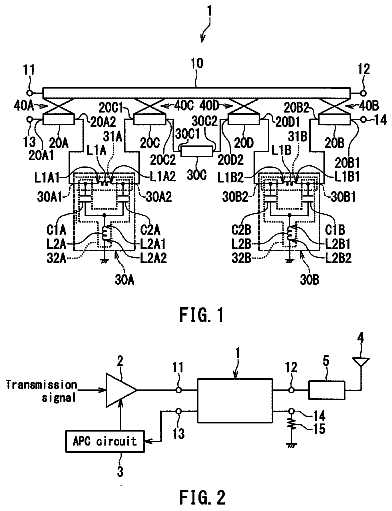
FIG. 1 is a circuit diagram illustrating the circuitry of a directional coupler according to a first embodiment of the invention.
FIG. 2 is a circuit diagram illustrating an example of use of the directional coupler according to the first embodiment of the invention.
FIG. 3 is a perspective view of the directional coupler according to the first embodiment of the invention.
FIG. 4 is a perspective internal view of a stack included in the directional coupler shown in FIG. 3 .
FIG. 5 is a perspective, partial internal view of the stack included in the directional coupler shown in FIG. 3 .
FIG. 6A to FIG. 6D are explanatory diagrams illustrating the respective top surfaces of the first to fourth dielectric layers of the stack included in the directional coupler shown in FIG. 3 .
FIG. 7A to FIG. 7D are explanatory diagrams illustrating the respective top surfaces of the fifth to eighth dielectric layers of the stack included in the directional coupler shown in FIG. 3 .
FIG. 8A to FIG. 8D are explanatory diagrams illustrating the respective top surfaces of the ninth to twelfth dielectric layers of the stack included in the directional coupler shown in FIG. 3 .
FIG. 9A to FIG. 9D are explanatory diagrams illustrating the respective top surfaces of the thirteenth to sixteenth dielectric layers of the stack included in the directional coupler shown in FIG. 3 .
FIG. 10A to FIG. 10D are explanatory diagrams illustrating the respective top surfaces of the seventeenth to twentieth dielectric layers of the stack included in the directional coupler shown in FIG. 3 .
FIG. 11A to FIG. 11D are explanatory diagrams illustrating the respective top surfaces of the twenty-first to twenty-fourth dielectric layers of the stack included in the directional coupler shown in FIG. 3 .
FIG. 12 is a circuit diagram illustrating the circuitry of a directional coupler of a first comparative example.
FIG. 13 is a characteristic diagram illustrating the frequency response of the insertion loss of the directional coupler of the first comparative example.
FIG. 14 is a characteristic diagram illustrating the frequency response of the coupling of the directional coupler of the first comparative example.
FIG. 15 is a characteristic diagram illustrating the frequency response of the isolation of the directional coupler of the first comparative example.
FIG. 16 is a characteristic diagram illustrating the frequency response of the return loss at the coupling port of the directional coupler of the first comparative example.
FIG. 17 is a characteristic diagram illustrating the frequency response of the insertion loss of the directional coupler according to the first embodiment of the invention.
FIG. 18 is a characteristic diagram illustrating the frequency response of the return loss at the input port of the directional coupler according to the first embodiment of the invention.
FIG. 19 is a characteristic diagram illustrating the frequency response of the coupling of the directional coupler according to the first embodiment of the invention.
FIG. 20 is a characteristic diagram illustrating the frequency response of the isolation of the directional coupler according to the first embodiment of the invention.
FIG. 21 is a characteristic diagram illustrating the frequency response of the directivity of the directional coupler according to the first embodiment of the invention.
FIG. 22 is a characteristic diagram illustrating the frequency response of the return loss at the coupling port of the directional coupler according to the first embodiment of the invention.
FIG. 23 is a circuit diagram illustrating the circuitry of a directional coupler according to a second embodiment of the invention. DETAILED DESCRIPTION OF THE PREFERRED EMBODIMENTS First Embodiment
Preferred embodiments of the present invention will now be described in detail with reference to the drawings. First, reference is made to FIG. 1 to describe the circuitry of a directional coupler according to a first embodiment of the invention. As shown in FIG. 1 , the directional coupler 1 according to the first embodiment includes a first port 11 , a second port 12 , a third port 13 , and a fourth port 14 . The directional coupler 1 further includes a main line 10 , a first subline section 20 A, a second subline section 20 B, a third subline section 20 C, a first matching section 30 A, and a second matching section 30 B. The main line 10 connects the first port 11 and the second port 12 . Each of the first to third subline sections 20 A, 20 B and 20 C is formed of a line configured to be electromagnetically coupled to the main line 10 . One of the third and fourth ports 13 and 14 is grounded via a terminator 15 having a resistance of, for example, 50 Ω.
The first subline section 20 A has a first end 20 A 1 and a second end 20 A 2 opposite to each other. The second subline section 20 B has a first end 20 B 1 and a second end 20 B 2 opposite to each other. The third subline section 20 C has a first end 20 C 1 and a second end 20 C 2 opposite to each other. The first matching section 30 A has a first end 30 A 1 and a second end 30 A 2 opposite to each other. The second matching section 30 B has a first end 30 B 1 and a second end 30 B 2 opposite to each other.
The first end 20 A 1 of the first subline section 20 A is connected to the third port 13 . The first end 30 A 1 of the first matching section 30 A is connected to the second end 20 A 2 of the first subline section 20 A. The first end 20 B 1 of the second subline section 20 B is connected to the second end 30 A 2 of the first matching section 30 A. The first end 30 B 1 of the second matching section 30 B is connected to the second end 20 B 2 of the second subline section 20 B. The first end 20 C 1 of the third subline section 20 C is connected to the second end 30 B 2 of the second matching section 30 B. The second end 20 C 2 of the third subline section 20 C is connected to the fourth port 14 .
The first matching section 30 A includes a first path 31 A connecting the first end 30 A 1 and the second end 30 A 2 , and a second path 32 A connecting the first path 31 A and the ground. The first path 31 A includes a first inductor L 1 A. The first inductor L 1 A has a first end L 1 A 1 and a second end L 1 A 2 opposite to each other. Here, of the two ends of the first inductor L 1 A, the first end L 1 A 1 is taken as the end closer to the first subline section 20 A, whereas the second end L 1 A 2 is taken as the end closer to the second subline section 20 B.
The second path 32 A includes a first capacitor C 1 A and a second inductor L 2 A connected in series. The second inductor L 2 A has a first end L 2 A 1 and a second end L 2 A 2 . In terms of circuitry, the first end L 2 A 1 is closest to the first path 31 A, and the second end L 2 A 2 is closest to the ground. The first capacitor C 1 A is provided between the first end L 1 A 1 of the first inductor L 1 A and the first end L 2 A 1 of the second inductor L 2 A. In the first embodiment, the second path 32 A further includes a second capacitor C 2 A provided between the second end L 1 A 2 of the first inductor L 1 A and the first end L 2 A 1 of the second inductor L 2 A. The second inductor L 2 A has an inductance of 0.1 nH or higher. The inductance of the second inductor L 2 A is preferably not higher than 7 nH.
The circuitry of the second matching section 30 B is similar to that of the first matching section 30 A. More specifically, the second matching section 30 B includes a first path 31 B connecting the first end 30 B 1 and the second end 30 B 2 , and a second path 32 B connecting the first path 31 B and the ground. The first path 31 B includes a first inductor L 1 R The first inductor L 1 B has a first end L 1 B 1 and a second end L 1 B 2 opposite to each other. Here, of the two ends of the first inductor L 1 B, the first end L 1 B 1 is taken as the end closer to the third subline section 20 C, whereas the second end L 1 B 2 is taken as the end closer to the second subline section 20 B.
The second path 32 B includes a first capacitor C 1 B and a second inductor L 2 B connected in series. The second inductor L 2 B has a first end L 2 B 1 and a second end L 2 B 2 . In terms of circuitry, the first end L 2 B 1 is closest to the first path 31 B, and the second end L 2 B 2 is closest to the ground. The first capacitor C 1 B is provided between the first end L 1 B 1 of the first inductor L 1 B and the first end L 2 B 1 of the second inductor L 2 B. In the first embodiment, the second path 32 B further includes a second capacitor C 2 B provided between the second end L 1 B 2 of the first inductor L 1 B and the first end L 2 B 1 of the second inductor L 2 B. The second inductor L 2 B has an inductance of 0.1 nH or higher. The inductance of the second inductor L 2 B is preferably not higher than 7 nH.
The main line 10 includes a first portion 10 A to be electromagnetically coupled to the first subline section 20 A, a second portion 10 B to be electromagnetically coupled to the second subline section 20 B, and a third portion 10 C to be electromagnetically coupled to the third subline section 20 C. Here, a portion of the main line 10 to be coupled to the first subline section 20 A, i.e., the first portion 10 A, and the first subline section 20 A in combination will be referred to as the first coupling section 40 A. A portion of the main line 10 to be coupled to the second subline section 20 B, i.e., the second portion 10 B, and the second subline section 20 B in combination will be referred to as the second coupling section 40 B. A portion of the main line 10 to be coupled to the third subline section 20 C, i.e., the third portion 10 C, and the third subline section 20 C in combination will be referred to as the third coupling section 40 C.
The strength of coupling of the first coupling section 40 A, the strength of coupling of the second coupling section 40 B, and the strength of coupling of the third coupling section 40 C will be defined as follows.
The strength of coupling of the first coupling section 40 A is the strength of coupling of the first subline section 20 A to the main line 10 , that is, the strength of coupling of the first subline section 20 A to the first portion 10 A of the main line 10 . Specifically, the strength of coupling of the first coupling section 40 A is expressed in terms of a ratio of the power of a high frequency signal appearing on the first subline section 20 A to the power of a high frequency signal supplied to the first portion 10 A.
The strength of coupling of the second coupling section 40 B is the strength of coupling of the second subline section 20 B to the main line 10 , that is, the strength of coupling of the second subline section 20 B to the second portion 10 B of the main line 10 . Specifically, the strength of coupling of the second coupling section 40 B is expressed in terms of a ratio of the power of a high frequency signal appearing on the second subline section 20 B to the power of a high frequency signal supplied to the second portion 10 B.
The strength of coupling of the third coupling section 40 C is the strength of coupling of the third subline section 20 C to the main line 10 , that is, the strength of coupling of the third subline section 20 C to the third portion 10 C of the main line 10 . Specifically, the strength of coupling of the third coupling section 40 C is expressed in terms of a ratio of the power of a high frequency signal appearing on the third subline section 20 C to the power of a high frequency signal supplied to the third portion 10 C.
The strength of coupling of the second coupling section 40 B may be higher than the strength of coupling of the first coupling section 40 A and the strength of coupling of the third coupling section 40 C.
Each of the first and second matching sections 30 A and 30 B is a circuit for performing impedance matching between a signal source and a load, assuming a situation in which one of the third and fourth ports 13 and 14 is grounded via a terminator serving as the load, and the other of the third and fourth ports 13 and 14 is connected with the signal source having an output impedance equal to the resistance of the terminator (e.g., 50 C 2 ). On the assumption of the above situation, the first and second matching sections 30 A and 30 B are each designed so that the reflection coefficient as viewed in the direction from one of the third and fourth ports 13 and 14 to the other has an absolute value of zero or near zero in the service frequency band of the directional coupler 1 . Each of the first and second matching sections 30 A and 30 B causes a change in the phase of a signal passing therethrough.
The circuitry of the directional coupler 1 , including element values, is preferably symmetric with respect to the second coupling section 40 B. However, the circuitry of the directional coupling 1 may be asymmetric if the degree of asymmetry is within an acceptable range.
In the following, we discuss the case where the circuitry of the directional coupler 1 is symmetric. In this case, the strength of coupling of the third coupling section 40 C is equal to the strength of coupling of the first coupling section 40 A. Further, the circuitry of the first matching section 30 A and that of the second matching section 30 B, including element values, are mutually symmetric with respect to the second coupling section 40 B. More specifically, the inductances of the first inductors L 1 A and L 1 B pairing up with each other are substantially equal to each other; the inductances of the second inductors L 2 A and L 2 B pairing up with each other are substantially equal to each other; the capacitances of the first capacitors C 1 A and C 1 B pairing up with each other are substantially equal to each other; and the capacitances of the second capacitors C 2 A and C 2 B pairing up with each other are substantially equal to each other. When signals of the same frequency pass through the first and second matching sections 30 A and 30 B, the first and second matching sections 30 A and 30 B cause changes of the same magnitude in the phase of those signals. The directional coupler 1 is bidirectional because the circuitry thereof is symmetric with respect to the second coupling section 40 B. As mentioned above, the inductances of two inductors pairing up with each other are “substantially equal to each other”, and ditto for the capacitances of two capacitors pairing up with each other. This means that errors in the inductances and capacitances resulting from manufacturing variances of the inductors and capacitors are tolerated.
In the first matching section 30 A shown in FIG. 1 , the first capacitor C 1 A is provided between the first end L 1 A 1 of the first inductor L 1 A and the first end L 2 A 1 of the second inductor L 2 A, and the second capacitor C 2 A is provided between the second end L 1 A 2 of the first inductor L 1 A and the first end L 2 A 1 of the second inductor L 2 A. In the second matching section 30 B shown in FIG. 1 , the first capacitor C 1 B is provided between the first end L 1 B 1 of the first inductor L 1 B and the first end L 2 B 1 of the second inductor L 2 B, and the second capacitor C 2 B is provided between the second end L 1 B 2 of the first inductor DB and the first end L 2 B 1 of the second inductor L 2 B. However, in terms of circuitry, the first and second capacitors C 1 A and C 2 A in the first matching section 30 A may be provided in a reversed arrangement from that in the example shown in FIG. 1 , and ditto for the first and second capacitors C 1 B and C 2 B in the second matching section 30 B. More specifically, in the first matching section 30 A, the first capacitor C 1 A may be provided between the second end L 1 A 2 of the first inductor L 1 A and the first end L 2 A 1 of the second inductor L 2 A, and the second capacitor C 2 A may be provided between the first end L 1 A 1 of the first inductor L 1 A and the first end L 2 A 1 of the second inductor L 2 A. In this case, in the second matching section 30 B, the first capacitor C 1 B is provided between the second end L 1 B 2 of the first inductor L 1 B and the first end L 2 B 1 of the second inductor L 2 B, and the second capacitor C 2 B is provided between the first end L 1 B 1 of the first inductor L 1 B and the first end L 2 B 1 of the second inductor L 2 B.
The operation and effects of the directional coupler 1 according to the first embodiment will now be described. The directional coupler 1 is usable in the following first and second modes of use. In the first mode of use, the first port 11 serves as the input port, the second port 12 serves as the output port, the third port 13 serves as the coupling port, and the fourth port 14 serves as the terminal port. In the first mode of use, the fourth port 14 is grounded via a terminator having a resistance of, for example, 50 Ω. In the second mode of use, the second port 12 serves as the input port, the first port 11 serves as the output port, the fourth port 14 serves as the coupling port, and the third port 13 serves as the terminal port. In the second mode of use, the third port 13 is grounded via a terminator having a resistance of, for example, 50 Ω.
In the first mode of use, a high frequency signal is received at the first port 11 and output from the second port 12 . The third port 13 outputs a coupling signal having a power that depends on the power of the high frequency signal received at the first port 11 .
In the first mode of use, a first, a second and a third signal path are formed between the first port 11 serving as the input port and the third port 13 serving as the coupling port. The first signal path passes through the first coupling section 40 A. The second signal path passes through the second coupling section 40 B and the first matching section 30 A. The third signal path passes through the third coupling section 40 C, the second matching section 30 B and the first matching section 30 A. When a high frequency signal has been received at the first port 11 , the coupling signal to be output from the third port 13 is a signal resulting from a combination of a signal having passed through the first signal path, a signal having passed through the second signal path, and a signal having passed through the third signal path. The coupling of the directional coupler 1 used in the first mode of use depends on the strength of coupling of each of the first to third coupling sections 40 A, 40 B and 40 C and the relationship among the phases of the signal having passed through the first signal path, the signal having passed through the second signal path, and the signal having passed through the third signal path.
In the first mode of use, a fourth, a fifth and a sixth signal path are formed between the second port 12 serving as the output port and the third port 13 serving as the coupling port. The fourth signal path passes through the first coupling section 40 A. The fifth signal path passes through the second coupling section 40 B and the first matching section 30 A. The sixth signal path passes through the third coupling section 40 C, the second matching section 30 B and the first matching section 30 A. The isolation of the directional coupler used in the first mode of use depends on the strength of coupling of each of the first to third coupling sections 40 A, 40 B and 40 C and the relationship among the phases of the signal having passed through the fourth signal path, the signal having passed through the fifth signal path, and the signal having passed through the sixth signal path.
In the second mode of use, a high frequency signal is received at the second port 12 and output from the first port 11 . The fourth port 14 outputs a coupling signal having a power that depends on the power of the high frequency signal received at the second port 12 .
In the second mode of use, a seventh, an eighth and a ninth signal path are formed between the second port 12 serving as the input port and the fourth port 14 serving as the coupling port. The seventh signal path passes through the third coupling section 40 C. The eighth signal path passes through the second coupling section 40 B and the second matching section 30 B. The ninth signal path passes through the first coupling section 40 A, the first matching section 30 A and the second matching section 30 B. When a high frequency signal has been received at the second port 12 , the coupling signal to be output from the fourth port 14 is a signal resulting from a combination of a signal having passed through the seventh signal path, a signal having passed through the eighth signal path, and a signal having passed through the ninth signal path. The coupling of the directional coupler 1 used in the second mode of use depends on the strength of coupling of each of the first, the second and the third coupling sections 40 A, 40 B and 40 C and the relationship among the phases of the signal having passed through the seventh signal path, the signal having passed through the eighth signal path, and the signal having passed through the ninth signal path.
In the second mode of use, a tenth, an eleventh and a twelfth signal path are formed between the first port 11 serving as the output port and the fourth port 14 serving as the coupling port. The tenth signal path passes through the third coupling section 40 C. The eleventh signal path passes through the second coupling section 40 B and the second matching section 30 B. The twelfth signal path passes through the first coupling section 40 A, the first matching section 30 A and the second matching section 30 B. The isolation of the directional coupler used in the second mode of use depends on the strength of coupling of each of the first to third coupling sections 40 A, 40 B and 40 C and the relationship among the phases of the signal having passed through the tenth signal path, the signal having passed through the eleventh signal path, and the signal having passed through the twelfth signal path.
Now, an example of use of the directional coupler 1 in the first and second modes of use will be described with reference to FIG. 2 . FIG. 2 is a circuit diagram illustrating an example of use of the directional coupler 1 . FIG. 2 illustrates a transmission circuit including the directional coupler 1 . The transmission circuit shown in FIG. 2 includes a power amplifier 2 , an automatic power control (APC) circuit 3 and an impedance matching element 5 , in addition to the directional coupler 1 .
The power amplifier 2 has an input, an output, and a gain control end. The input of the power amplifier 2 receives a transmission signal, which is a high frequency signal. The output of the power amplifier 2 is connected to the first port 11 of the directional coupler 1 .
The APC circuit 3 has an input and an output. The input of the APC circuit 3 is connected to the third port 13 of the directional coupler 1 . The output of the APC circuit 3 is connected to the gain control end of the power amplifier 2 .
The second port 12 of the directional coupler 1 is connected to an antenna 4 via the impedance matching element 5 . The impedance matching element 5 is an element for performing impedance matching between the transmission circuit and the antenna 4 in order to sufficiently reduce the level of a reflected wave signal resulting from the transmission signal reflected at the antenna 4 . The fourth port 14 of the directional coupler 1 is grounded via the terminator 15 .
Next, the first mode of use of the directional coupler 1 in the transmission circuit shown in FIG. 2 will be described. In the first mode of use, the transmission signal amplified by the power amplifier 2 is received at the first port 11 and output from the second port 12 . The third port 13 outputs a coupling signal having a power that depends on the level of the transmission signal received at the first port 11 . The transmission signal output from the second port 12 goes through the impedance matching element 5 and is emitted from the antenna 4 . The coupling signal output from the third port 13 is received at the APC circuit 3 . In accordance with the level of the coupling signal output from the third port 13 , the APC circuit 3 controls the gain of the power amplifier 2 so that the power amplifier 2 provides an output signal of approximately constant level.
Next, the second mode of use of the directional coupler 1 in the transmission circuit shown in FIG. 2 will be described. In the second mode of use, the directional coupler 1 is used to detect the level of a reflection wave signal resulting from the transmission signal reflected at the antenna 4 . In the second mode of use, the reflected wave signal is the high frequency signal to be received at the directional coupler 1 . The reflected wave signal is received at the second port 12 and output from the first port 11 . Thus, in the second mode of use, the second port 12 serves as the input port, the first port 11 serves as the output port, the fourth port 14 serves as the coupling port, and the third port 13 serves as the terminal port. In the second mode of use, the third port 13 is grounded via a terminator. The fourth port 14 is connected with a power detector (not illustrated). The fourth port 14 outputs a coupling signal having a power that depends on the power of the reflected wave signal received at the second port 12 . The non-illustrated power detector detects the level of the coupling signal. The information on the level of the coupling signal is used to adjust the characteristics of the impedance matching element 5 so as to sufficiently reduce the level of the reflected wave signal.
The level of the reflected wave signal received at the directional coupler 1 is lower than that of the transmission signal received at the directional coupler 1 . Thus, sufficient isolation is required of the directional coupler 1 not only in the first mode of use but also in the second mode of use.
The description continues in the full USPTO document.
About 7,343 words. The USPTO PDF has it with every drawing.
Fees are due 3.5, 7.5 and 11.5 years after grant. This patent expired on February 13, 2026, so the fee marked "not paid" was the one that went unpaid.
DIRECTIONAL COUPLER
Filed Jun 2016 · published Feb 2017Directional coupler
Filed Jun 2016 · granted Feb 2018Earlier publications, parents and continuations. None of them can still be enforced, or this patent would not be listed.
Prior art cited by the examiner or applicant. Useful when you check your own idea for novelty.
Everything on this page comes from the documents linked above.