Field of the invention
The present invention relates to: an electric near-field probe having a function of transmission and reception capable of exciting a crystal having a piezoelectric effect, that is, a piezoelectric crystal, by an external electric field and of detecting a piezoelectric effect signal generated from the excited piezoelectric crystal; a control system for the same; and a piezoelectric crystal detector employing the electric near-field probe and the control system for the same.
Background of the invention
It is known that when an alternating electric field is applied, a piezoelectric crystal mechanically vibrates at a particular frequency. Then, even after application of the alternating electric field is stopped, the mechanical vibration is maintained with attenuation by a piezoelectric effect and thereby generates a new alternating electric field.
Thus, by detecting the newly generated alternating electric field as a piezoelectric effect signal with an electric field probe (an electric field type antenna), the presence or absence of a piezoelectric crystal can be detected in a non-contact (e.g., Non-patent Document 1).
At that time, in a case that an electric field probe having a function of both transmission and reception capable of also applying an alternating electric field to the piezoelectric crystal is employed as the electric field probe, detection of a piezoelectric crystal can efficiently be achieved.
Such piezoelectric crystals include illicit drugs such as cocaine and stimulant. Then, as a specific example that an electric field probe having a function of both transmission and reception is applied to detection of an illicit drug, a technique is proposed that: a capacitor constructed from two metal plates is employed and then an object to be inspected such as a bag is inserted between the metal plates; and then an alternating electric field is applied between the metal plates and thereby a piezoelectric effect signal from an illicit drug such as cocaine and stimulant is received so that a concealed illicit drug is detected in a sealed state in a non-contact (e.g., Patent Document 1). PRIOR ART REFERENCE Patent Document
Patent Document 1: U.S. Pat. No. 7,132,942 Non-Patent Document
Non-patent Document 1: T. Rayner et al., Narcotics detection using piezoelectric ringing, the international society for optics and photonics Proc., 1997, vol. 2936, pp. 31-38 SUMMARY OF THE INVENTION Problems to be Solved by the Invention
Nevertheless, in the case of conventional art, as described above, it has not been expected that measurement is performed in a state that the entirety of an object to be inspected is inserted between the metal plates of a capacitor. Thus, size increase of the electric field probe and hence size increase of the detector have been unavoidable. Further, a to-be-inspected object having a size not insertable between the metal plates of the capacitor cannot be inspected.
Further, natural cocaine or the like contains an impurity also. This has caused another problem that sufficient detection sensitivity cannot be obtained in the conventional art. Thus, this technique has not been used in practice.
Thus, an object of the present invention is to provide: an electric field probe having a small size and a light weight and yet having a transmission and reception function of capable of applying an alternating electric field to a piezoelectric crystal so as to excite the piezoelectric crystal and also detecting a piezoelectric effect signal with a sufficient sensitivity; a control system for this; and a piezoelectric crystal detector. Means for Solving the Problem
For resolving the above-mentioned problems, the present inventor has conceived that in contrast to the conventional art wherein measurement is performed in a state that an object to be inspected is inserted between the metal plates of a capacitor, when a capacitor in which the distance between the metal plates is reduced to reduce size and weight is employed for fabricating an electric near-field probe having a function of transmission and reception, size and weight reduction of the electric field probe can be achieved.
Specifically, attention has been focused on a fact that when a voltage is applied to a capacitor, a leakage electric field occurs in the outside of the metal plates. Then, it has been conceived that when an electric near-field caused by the leakage electric field is transmitted so that the piezoelectric crystal is vibrated at a particular resonance frequency and then an alternating electric field, that is, a piezoelectric effect signal, generated by the vibration is detected, the piezoelectric effect signal can be detected with a sufficient sensitivity without the necessity of inserting the to-be-inspected object between the metal plates. Hence size and weight reduction of the electric field probe can be achieved.
However, when the leakage electric field is to be used, simultaneously to occurrence of the electric near-field, an alternating magnetic near-field is generated in some cases. The generated alternating magnetic near-field causes vibration in the metal plates or the like, and thereby induces an alternating magnetic field signal (magnetic ringing) so as to disturb the receiving of the piezoelectric effect signal. This causes a possibility of degradation in the detection sensitivity.
Thus, the present inventor has investigated means of suppressing occurrence of the alternating magnetic field signal in the above-mentioned electric near-field probe. As a result, with focusing attention on the inductor of an LCR resonance circuit provided in the electric near-field probe, it has been conceived that an inductor constructed such that a lead wire is wound around a toroidal core is to be employed.
The LCR resonance circuit is constructed such that a capacitor (C) constructed by inserting air or a dielectric material between two parallel metal plates serving as conductors is connected to an inductor (L) in series. Here, R indicates a resistance component contained in the inductor, the capacitor, a wiring, a transmission amplifier, and the like.
Then, in the LCR resonance circuit, when an inductor constructed such that a lead wire is wound around a toroidal core is employed, the magnetic field generated from the inductor is confined so that leakage of the magnetic field can sufficiently be suppressed. As a result, occurrence of an alternating magnetic field signal (magnetic ringing) can be suppressed.
An electric near-field probe having the above-mentioned LCR resonance circuit can have a remarkably small size and a remarkably light weight in comparison with an electric field probe of the conventional art. Further, as described above, a piezoelectric crystal can be excited by an electric near-field generated by a leakage electric field and, at the same time, a piezoelectric effect signal can be detected in a state that leakage of a magnetic field is sufficiently suppressed. Thus, when the electric near-field probe is held by the hand like a handy type metal detector and then merely brought close to an object to be inspected such as clothes and a bag, the presence or absence of a piezoelectric crystal can be detected.
That is, the invention according to claim 1 is an electric near-field probe comprising a series resonance circuit that is constructed such that a capacitor constructed such that a space between two metal plates arranged in parallel to each other is filled with a dielectric material or air and an inductor constructed such that a lead wire is wound around a toroidal core, are connected in series and that has a predetermined resonance frequency, wherein an electric near-field originating from a leakage electric field from the capacitor generated when an alternating voltage is applied to the series resonance circuit is transmitted to a piezoelectric crystal so that the piezoelectric crystal is excited and, at the same time, a piezoelectric effect signal generated from the excited piezoelectric crystal is received by the capacitor so that the piezoelectric effect signal is detected by the series resonance circuit.
Next, in order to improve the detection sensitivity further, the present inventor has investigated a capacitor structure more advantageous in transmission of the leakage electric field and detection of the piezoelectric effect signal. As a result, it has been confirmed that when an opening part is provided near the center of the metal plate opposing the piezoelectric crystal, the electric field intensity immediately above the probe center can be increased and the detection sensitivity can be improved further.
That is, the invention according to claim 2 is the electric near-field probe according to claim 1 , wherein an opening part is provided in a center portion of the metal plate opposing the piezoelectric crystal among the two metal plates constituting the capacitor.
Next, the present inventor has investigated a series resonance circuit (including a series resonance circuit whose equivalent circuit becomes the same) that permits efficient detection in the electric near-field probe. As a result, it has been confirmed that when a plurality of series resonance circuits having different resonance frequencies are provided, piezoelectric crystals having different resonance frequencies depending on the kind, the particle size, or the like can efficiently be detected by using one electric near-field probe.
That is, the invention according to claim 3 is the electric near-field probe according to claim 1 or 2 , wherein the series resonance circuit is constructed from a plurality of series resonance circuits having different resonance frequencies.
Then, in such an electric near-field probe including a plurality of series resonance circuits, when an alternating voltage of a frequency corresponding to each resonance frequency is inputted, resonance can easily be achieved at each of the different resonance frequencies.
That is, the invention according to claim 4 is the electric near-field probe according to claim 3 , wherein in each of the plurality of series resonance circuits, when an alternating voltage of a resonance frequency corresponding to each series resonance circuit is inputted, resonance is achieved.
Further, also when a modulated alternating voltage is inputted to an electric near-field probe having a series resonance circuit constructed from a plurality of series resonance circuits, resonance can easily be achieved at different resonance frequencies.
That is, the invention according to claim 5 is the electric near-field probe according to claim 3 , wherein in the plurality of series resonance circuits, when a modulated alternating voltage is inputted, resonance is achieved.
The electric near-field probe according to the present invention is basically used in the outside of an electromagnetic shield. Then, when the electric near-field probe is used in the outside of an electromagnetic shield as such, the electric near-field probe becomes subject to control under Article 100 of Radio Act. Thus, the electric field intensity at a 30-m away position need be limited to 100 μV/m or lower.
Thus, in the electric near-field probe according to the present invention, it is preferred that the electric field intensity at a distance is suppressed to the regulation value or lower and yet the electric field intensity in the vicinity of the probe is increased as high as possible.
As a result of investigation, the present inventor has confirmed that when an electric near-field probe of gradio structure type constructed such that two capacitors having the same shape and the same size are horizontally arranged and aligned with a wiring connected in opposite polarity to each other is employed, a sufficient electric field intensity can be ensured and yet the electric fields at a distance can cancel out.
That is, the invention according to claim 6 is the electric near-field probe according to claim 1 , wherein two capacitors having the same shape and the size are arranged and aligned in parallel to each other, then an inductor having the same shape and the size is connected to each capacitor, and then the capacitors are connected to each other in opposite polarity so as to be constructed in a gradio structure type.
In some cases, the electric near-field probe is used in an electromagnetic shielding environment. In such cases, a noise from the outside is reduced by the electromagnetic shielding environment. On the other hand, a noise from the reception circuit is not reduced. Thus, there is a possibility that the noise from the reception circuit becomes dominant and degrades the receiving sensitivity.
Thus, the present inventor has confirmed that when the series resonance circuit is constructed such that the amplification factor for the noise in the reception circuit at the time of receiving is reduced and yet the amplification factor for the piezoelectric effect signal received by the electric near-field probe is maintained large, degradation in the receiving sensitivity is not caused.
That is, the invention according to claim 7 is the electric near-field probe according to claim 1 , wherein the series resonance circuit is provided with an amplification factor changing circuit constructed such that an amplification factor for a noise in a reception circuit can be reduced and yet an amplification factor for the piezoelectric effect signal received by the electric near-field probe can be maintained large.
Further, the present inventor has confirmed that when a series resonance circuit is provided such as to reduce a transient phenomenon occurring in the electric near-field probe after termination of a transmission signal, the receiving sensitivity can be improved.
That is, the invention according to claim 8 is the electric near-field probe according to claim 1 , wherein the series resonance circuit is provided with an amplifier circuit for transmission constructed such as to reduce a fall time of a transient phenomenon occurring in the electric near-field probe after termination of a transmission signal.
Here, the amplification factor changing circuit and the amplifier circuit for transmission described above may be applied to a probe, especially, an electric near-field probe, constructed from another resonance circuit and then a similar effect can be obtained.
The above-mentioned electric near-field probe is controlled by an electric near-field probe control system described below.
That is, the invention according to claim 9 is an electric near-field probe control system for controlling the electric near-field probe according to any one of claims 1 to 8 , wherein an alternating voltage is applied to the series resonance circuit having a predetermined resonance frequency so that an electric near-field originating from a leakage electric field generated by the capacitor is transmitted from the electric near-field probe so as to excite the piezoelectric crystal and, on the other hand, a piezoelectric effect signal generated from the excited piezoelectric crystal is received by the capacitor so that presence or absence or a property of the piezoelectric crystal is detected by the series resonance circuit.
The above-mentioned electric near-field probe control system can be contained in the form of a small and light-weight system. Then, a piezoelectric crystal can sufficiently be excited by an electric near-field originating from a leakage electric field and hence a piezoelectric effect signal can be obtained with sufficient detection sensitivity.
Further, the invention according to claim 10 is a piezoelectric crystal detector comprising the electric near-field probe according to any one of claims 1 to 8 and the electric near-field probe control system according to claim 9 and thereby detects presence or absence or a property of a piezoelectric crystal.
This is a piezoelectric crystal detector having: an electric near-field probe constructed in a small size and a light weight; and an electric near-field probe control system. Thus, a portable piezoelectric crystal detector can be provided that can easily be carried and can perform high-accuracy measurement in a short time.
Further, the invention according to claim 11 is the piezoelectric crystal detector according to claim 10 , serving as an illicit drug detector.
As described above, in the electric near-field probe according to the present invention, when the probe is held by the hand and then held over an object like a handy type metal detector, a piezoelectric effect signal can be obtained with sufficient detection sensitivity. Thus, illicit drugs such as cocaine and stimulant composed of piezoelectric crystals can efficiently be detected.
Further, the invention according to claim 12 is the piezoelectric crystal detector according to claim 10 , employed in a non-contact key system.
By constructing a non-contact key system in which unlock is performed when a piezoelectric crystal key in which a piezoelectric crystal is buried is hang over a piezoelectric crystal detector, high security performance can be provided.
Further, the invention according to claim 13 is a piezoelectric crystal detector, wherein a plurality of the electric near-field probes according to any one of claims 1 to 8 are arranged between the plate electrodes arranged in parallel to each other.
Further, the present inventor has investigated a piezoelectric crystal detector in which even for piezoelectric crystals distributed broadly, a piezoelectric effect signal can be received with a high sensitivity so that the piezoelectric crystals can efficiently be detected and searched out.
As such a piezoelectric crystal detector for detecting piezoelectric crystals distributed broadly, in the conventional art, there has been a piezoelectric crystal detector for performing transmission and reception by using plate electrodes (parallel plate electrodes) arranged in parallel to each other. Nevertheless, it has been difficult so far to receive a piezoelectric effect signal with sufficiently high sensitivity.
The present inventor has found that when a plurality of the electric near-field probes according to the present invention are arranged between the parallel plate electrodes and then parallel plate electrodes are used for transmission and each of the plurality of electric near-field probes having been arranged is used for receiving, the piezoelectric crystals distributed broadly can efficiently be detected and searched out.
That is, when an electric field is transmitted from such parallel plate electrodes, the electric field can be generated broadly. Thus, even piezoelectric crystals distributed broadly can sufficiently be excited so that a piezoelectric effect signal can be generated. Then, it has been found that when the piezoelectric effect signal is received by a plurality of the electric near-field probes according to the present invention, the piezoelectric effect signal can be received with a high sensitivity and hence the piezoelectric crystals can efficiently be detected and searched out, in comparison with a case that receiving is performed by parallel plate electrodes.
Further, in a case that receiving is performed by parallel plate electrodes, even when a piezoelectric crystal is moved in a horizontal direction so that the distance from the parallel plate electrodes is changed, the receiving sensitivity does not substantially vary. However, in a case that receiving is performed by an electric near-field probe, it has been found that when a piezoelectric crystal is moved in a perpendicular direction so that the distance from the parallel plate electrodes is changed, the receiving sensitivity varies. Thus, the receiving sensitivity is improved at a position close to the electric near-field probe so that the piezoelectric crystal can more efficiently be detected and searched out.
Then, the piezoelectric crystal detector having the above-mentioned configuration can be constructed such that a reception circuit is connected to each of the plurality of electric near-field probes and then a transmission circuit is connected to the parallel plate electrodes. Since these reception circuits and transmission circuit are inexpensive, the piezoelectric crystal detector can be provided at a low cost.
Here, these reception circuits and transmission circuit may be provided individually or, alternatively, may be provided in an integrated manner. Further, the entirety may be constructed and integrated into one transmission and reception circuit. In a case that the individual circuits are provided individually, a piezoelectric crystal detector having higher detection sensitivity can be provided. On the other hand, in a case that the individual circuits are provided in an integrated manner, a more compact piezoelectric crystal detector can be provided.
Further, when the transmission and reception circuit is used as a circuit connected to the electric near-field probe, in cooperation with the electric field transmitted from the electric near-field probe, the electric field spreads at a higher intensity over a wider region. Thus, piezoelectric crystals in a wider range can sufficiently be excited and hence a piezoelectric effect signal can more efficiently be received with a high sensitivity. Effect of the Invention
According to the present invention, it can provide: an electric field probe having a small size and a light weight and yet having a transmission and reception function of capable of applying an alternating electric field to a piezoelectric crystal so as to excite the piezoelectric crystal and also detecting a piezoelectric effect signal with a sufficient sensitivity; a control system for this; and a piezoelectric crystal detector.
Brief description of the drawings
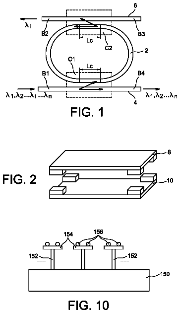
FIG. 1 is a diagram showing an example of configuration of a single frequency type electric near-field probe.
FIG. 2 is a diagram showing an example of configuration of a plural frequency type electric near-field probe.
FIG. 3 is a circuit diagram showing an example of configuration of a gradio structure type electric near-field probe.
FIG. 4 is a circuit diagram showing an example of configuration of a single frequency type electric near-field probe and a control system for this.
FIG. 5 is a circuit diagram showing an example of configuration of a plural frequency type electric near-field probe and a control system for this.
FIG. 6 is a circuit diagram showing another example of configuration of a plural frequency type electric near-field probe and a control system for this.
FIG. 7 is a circuit diagram showing another example of configuration of a plural frequency type electric near-field probe and a control system for this.
FIG. 8 is a circuit diagram showing an example of configuration of a high-sensitivity receiving type electric near-field probe and a control system for this.
FIG. 9 is a diagram describing an example of a pulse sequence for single frequency.
FIG. 10 is a diagram describing an example of a pulse sequence for plural frequency.
FIG. 11 is a schematic diagram of a frequency-modulated pulse sequence.
FIG. 12 is a circuit diagram showing an example of configuration of a transmission amplifier.
FIG. 13 is a diagram showing a voltage waveform of a sine burst wave generated in a resonance circuit by using a transmission amplifier shown in FIG. 12 .
FIG. 14 is a block diagram showing a configuration of a piezoelectric crystal detector according to an embodiment of the present invention.
FIG. 15 is a perspective view of a piezoelectric crystal detector according to an embodiment of the present invention.
FIG. 16 is a diagram showing electric field intensity generated in the vicinity of a capacitor of an electric near-field probe.
FIG. 17 is a waveform obtained when a waveform of an excitation transmission pulse (a sine burst wave) from an electric near-field probe is received by an electric field probe installed in the vicinity of an electric near-field probe.
FIG. 18 is a diagram showing an example of a waveform of a transmission pulse in a case that two different excitation transmission pulses (sine burst waves) are transmitted simultaneously.
FIG. 19 is a diagram showing an example of a waveform of a modulated transmission pulse (a sine burst wave) having undergone frequency modulation.
FIG. 20 is a diagram showing an example of measurement results of a relation between electric field intensity and an electric near-field probe.
FIG. 21 is a diagram showing a relation between the frequency of a piezoelectric effect signal and the size (the width) of synthetic quartz.
FIG. 22 is a diagram showing a time domain signal (before phase detection) of a piezoelectric effect signal from a plurality of Rochelle crystals.
FIG. 23 is a diagram showing a time domain signal (after phase detection) of a piezoelectric effect signal from a plurality of Rochelle crystals.
FIG. 24 is a diagram showing a frequency domain signal of a piezoelectric effect signal from a plurality of Rochelle crystals.
FIG. 25 is a diagram showing a piezoelectric effect signal received from two Rochelle salts having different resonance frequencies by an electric near-field probe having two resonance frequencies.
FIG. 26 is a diagram showing a piezoelectric effect signal received from a plurality of Rochelle salts having different resonance frequencies by an electric near-field probe having two resonance frequencies.
FIG. 27 is a diagram showing a piezoelectric effect signal received from a plurality of Rochelle salts excited by using a frequency-modulated sine burst wave.
FIG. 28 is a diagram showing relations between the intensity of a piezoelectric effect signal and the distance from an electric near-field probe in electric near-field probes of gradio structure type and of normal type.
FIG. 29 is a perspective view schematically showing an example of a piezoelectric crystal detector in which plurality of electric near-field probes are arranged.
FIG. 30 is a diagram showing a piezoelectric effect signal received by using a piezoelectric crystal detector shown in FIG. 29 .
FIG. 31 is a diagram showing an example of measurement results of magnetic ringing in electric near-field probes whose inductors are different from each other.
FIG. 32 is a diagram showing an example of measurement results of a piezoelectric effect signal in electric near-field probes whose inductors are different from each other.
FIG. 33 is a diagram showing the shapes of a sine burst wave generated from an electric near-field probe in a case that a human body is present in the vicinity and in a case that a human body is not present.
Mode of implementing the invention
The present invention is described below in detail on the basis of an embodiment with reference to the drawings.
1. Electric Near-Field Probe
First, an electric near-field probe is described below.
Single Frequency Type
FIG. 1 shows the configuration of a single frequency type electric near-field probe of the present invention. Part (a) is a schematic diagram (the right part is a top view and the left part is a sectional view). Part (b) is a sectional view schematically showing the configuration of a capacitor 11 shown in part (a).
As shown in FIG. 1( a ) , a single frequency type electric near-field probe 1 has an LCR resonance circuit using one capacitor 11 and one inductor 12 . The capacitor 11 and the inductor 12 are connected in series and then connected to a transmission and reception circuit through a coaxial cable 13 . One end of the inductor 12 is connected to the ground and hence maintained at a reference potential.
a. Capacitor
As the capacitor 11 , a capacitor of parallel plate type preferable for formation of an electric field is employed. Specifically, the capacitor is constructed such that air or a dielectric material (polytetrafluoroethylene such as Teflon (registered trademark), a glass epoxy resin, or the like) is inserted between two metal plates fixed with a constant interval in between. By suitably changing the distance between the metal plates, the area, the kind of the dielectric material, the capacitance (C) of the capacitor can be adjusted.
Here, in the capacitor 11 shown in FIG. 1( b ) , numerals 111 a and 111 b indicate metal plates fabricated from a copper foil, numeral 112 indicates a dielectric material of polytetrafluoroethylene, and numeral 113 indicates a protection plate fabricated from plastics. When the protection plate 113 side is caused to oppose an object to be inspected, an electric near-field originating from a leakage electric field of the capacitor 11 is transmitted to a piezoelectric crystal serving as an object of measurement. Further, after the termination of transmission, a piezoelectric effect signal from the piezoelectric crystal is detected. The capacitor 11 having such a configuration can be fabricated, for example, by employing a microwave substrate fabricated by Polyflon Company (trade name: Cuflon) or the like.
In the above-mentioned capacitor 11 , an opening part 111 c is provided in the center portion of the metal plate 111 a . As such, when the opening part 111 c is provided in the center portion of the metal plate 111 a opposing the piezoelectric crystal, the electric field intensity immediately above the probe center can be increased and, at the same time, the detection sensitivity can also be improved further. Here, the size and the shape of the metal plate 111 a are not limited to particular ones. However, for example, in the case of a rectangular shape, a size of approximately 80×80 mm is preferable. Further, the size and the shape of the opening part 111 c provided in the metal plate 111 a like this are also not limited to particular ones. However, in the case of the metal plate 111 a having the above-mentioned size, it is preferable that the opening part 111 c is formed in a rectangular shape having a size of approximately 10×10 mm.
Here, a variable capacitor whose capacitance can be changed may be connected in parallel to the capacitor 11 . In this case, the resonance frequency can suitably be adjusted in one electric near-field probe 1 . This widens the range of application and hence is preferable.
b. Inductor
The inductor 12 is constructed such that a lead wire is wound around a toroidal core. When the fashion of winding of the lead wire is adjusted, the inductor 12 having a desired inductance (L) can be formed.
When the toroidal core is employed, a magnetic field generated from the inductor 12 can be confined so that leakage of the magnetic field can sufficiently be suppressed. Thus, occurrence of an alternating magnetic field signal (magnetic ringing) serving as an unnecessary signal at the time of measurement can be suppressed so that a piezoelectric effect signal can be detected with a high sensitivity.
c. Resonance Frequency
The electric near-field probe 1 having the above-mentioned configuration can perform both transmission of an alternating electric field and receiving of a piezoelectric effect signal. Then, on the basis of the inductance (L), the capacitance (C), and the resistor (R), a resonance frequency corresponding to an object piezoelectric crystal is set up. For example, in the case of inductance L=80.8 pH, capacitance C=167 pF, and R=6.8Ω, the resonance frequency is set to be 1.37 MHz. Here, the resonance frequency of the object piezoelectric crystal varies depending on the shape and the kind of the piezoelectric crystal. Even in piezoelectric crystals of the same kind, the resonance frequency varies depending on the size of the crystal grains or the like. Specifically, a large particle in the order of several centimeters has a resonance frequency in kHz band and a small particle in the order of several millimeters has a resonance frequency in MHz band.
Plural Frequency Type
Next, a plural frequency type electric near-field probe is described below. In the plural frequency type electric near-field probe, two or more parallel plate type capacitors like that described above are employed and then an inductor using a toroidal core is attached independently to each capacitor. FIG. 2 shows outlines of an electric near-field probe having two resonance frequencies (the right part is a top view and the left part is a sectional view).
As an example, an electric near-field probe 2 having two different resonance frequencies is constructed from combinations between a capacitor 21 a and an inductor 22 a and between a capacitor 21 b and an inductor 22 b so that two resonance circuits whose resonance frequencies are different are formed. Then, each resonance circuit is connected to the transmission and reception circuit through a coaxial cable 23 a or 23 b . Here, the resonance frequencies are set suitably into appropriate frequencies in accordance with the application. Here, in FIG. 2 , numeral 24 indicates a metal plate fabricated from a copper foil and numeral 25 indicates a dielectric material of polytetrafluoroethylene.
When a plurality of series resonance circuits having different resonance frequencies are provided, as described above, a plurality of piezoelectric crystals having different resonance frequencies depending on the kind, the particle size, or the like can efficiently be detected by using one electric near-field probe.
Gradio Structure Type
Next, a gradio structure type electric near-field probe is described below. FIG. 3 shows outlines of a gradio structure type electric near-field probe (the right part is a top view and the left part is a sectional view). In a gradio structure type electric near-field probe 4 , capacitors 41 a and 41 b having the same shape and size are aligned in parallel and then connected in opposite polarity to each other. Specifically, two identical capacitors of parallel plate type are aligned in a plane and then connected such that the relation of connection to the front and the rear surface of each capacitor becomes opposite to each other. By virtue of this, a gradio structure is constructed. Here, in FIG. 3 , numeral 43 indicates a coaxial cable, numeral 44 indicates a metal plate fabricated from a copper foil, and numeral 45 indicates a dielectric material of polytetrafluoroethylene.
When the connection is in opposite polarity to each other, leakage electric near-fields from the two capacitors 41 a and 41 b aligned in parallel are in opposite directions to each other and hence the electric fields cancelled out at a distance. Thus, an electric near-field probe in which the electric field intensity at a distance is attenuated to the regulation value or lower and yet attenuation of the electric field intensity in the vicinity is avoided as much as possible can be provided within the regulation range by Radio Act.
At that time, when an inductor 42 a , a capacitor 41 a , a capacitor 41 b , and an inductor 42 b are connected in this order, in the two electrodes of the capacitor, similarly to the above-mentioned single frequency type, the voltages oscillate relative to the ground so that resonance can be obtained.
2. Control System
Next, a basic configuration of a control system for controlling the electric near-field probe is described below.
Single Frequency Control Circuit
FIG. 4 is a circuit diagram showing an example of configuration of a single frequency type electric near-field probe and a control system for this. A piezoelectric crystal detector is constructed from the electric near-field probe and a circuit (a control circuit) of the control system.
For example, in the control circuit, a commercially available FPGA development board is employed. Then, a pulse generating circuit, a signal processing circuit, and a signal acquiring circuit are constructed in the inside of the FPGA so that the control circuit can be fabricated.
As shown in FIG. 4 , a transmission signal is outputted from a digital input/output terminal of the FPGA, then amplified by a transmission amplifier, and then provided through a low-pass filter and a cross diode to the electric near-field probe. At that time, the electric near-field probe, the cross diode, and the transmission amplifier constitute a series resonance circuit.
In association with the voltage amplification by the resonance circuit, the voltage across both ends of the capacitor becomes Q (10 to 150)-fold the output voltage of the transmission amplifier. Thus, the output intensity of the electric near-field can be increased further.
Further, at the time of receiving, a band-pass filter is provided so that an alternating electric field near the resonance frequency of the electric near-field probe is received. This reduces an external noise having a frequency component outside the band.
Here, in order to increase the voltage amplification factor at the time of transmission, it is preferable that a D-class amplifier circuit having a low power consumption within the amplifier and capable of low-impedance output is employed as the transmission amplifier. Then, in association with this, as shown in FIG. 4 , it is preferable that a low-pass filter is arranged immediately behind the transmission amplifier so that leakage of radio waves of harmonic components of the excitation frequency from the electric near-field probe including the cable is prevented.
Next, when the cross diode of FIG. 4 is arranged immediately behind the low-pass filter of the series resonance circuit, a transient phenomenon occurring in the electric near-field probe after transmission of a transmission pulse can be reduced. That is, as the voltage acting on the electric near-field probe after transmission attenuates and approaches the forward threshold voltage of the diode, the resistance component of the diode varies nonlinearly in accordance with the applied voltage and thereby increases rapidly. Thus, the energy accumulated in the resonance circuit is efficiently consumed by the resistance of the diode and hence a transient phenomenon can be reduced. Further, also in order that, at the time of receiving, the transmission amplifier of low impedance may be disconnected so that the configuration may be changed into a resonance circuit having a receiving amplifier, the cross diode need be arranged.
Further, in order that the output from the transmission amplifier may be not transferred to the receiving side, a transmission/reception changeover switch constructed from a semiconductor relay or a reed relay may be employed. The cross diode arranged immediately in front of the receiving amplifier is inserted for the purpose of clamping the signal when a large voltage acts on the receiving amplifier.
As the receiving amplifier, one having an amplification factor of approximately 50 to 100 dB is employed. Then, for the purpose of reducing a subsequent noise and preventing aliasing in an ADC, a band-pass filter or a low-pass filter is employed.
The output of the ADC is transferred from the digital input/output terminal to the FPGA and then, in the inside, lead to a circuit for accumulating the piezoelectric effect signal and an FFT circuit for calculating a frequency spectrum.
When a high-speed ADC (10 to 100 MHz) of parallel type is employed as the ADC, in the inside of the FPGA, phase detection is performed on the output signal of the ADC so that the signal is decomposed into two components whose phases are different by 90 degrees and then measurement is performed.
Further, when a low-speed ADC (1 to 3 MHz) of serial type is employed, the sampling frequency is set to be 4/(odd number)-fold the excitation frequency so that the signal can be decomposed into two components whose phases are different by 90 degrees by a band-pass sampling method.
The description continues in the full USPTO document.
 Lapsed, fee not paid13 drawings