BACKGROUND OF THE INVENTION Field of the Invention
The present invention relates to a thin film piezoelectric element that substantially does not contain lead. The present invention also relates to a piezoelectric actuator, a liquid ejection head, a liquid ejection device, a vibration correction mechanism, a variable optical component, a movable optical component, an optical instrument, an imaging device, an optical switch, a micromirror device, an ultrasonic probe, an ultrasonic inspection device, an acoustic component, an angular velocity sensor, a vibration power generation device, a surface acoustic wave generating device, a piezoelectric shutter and an electronic instrument. Description of the Related Art
A thin film piezoelectric element normally comprises a lower electrode, an upper electrode and a piezoelectric film sandwiched between the electrodes. A piezoelectric film is formed by a polycrystalline substance prepared from a ferroelectric metal oxide. A piezoelectric film generally contains as principal ingredient ABO.sub.3 type perovskite-type metal oxide such as lead zirconate titanate (PZT). However, since PZT contains lead as A-site element, its adverse influence on the environment is regarded as a problem that needs to be dissolved. For this reason, there is a demand for piezoelectric film containing no lead (lead-free piezoelectric film).
Barium zirconate titanate film is known as lead-free piezoelectric film. Japanese Patent Application Laid-Open No. 2011-243722 describes an achievement of suppressing cracks of piezoelectric film by adding manganese oxide to barium zirconate titanate by not less than 2 mol % and not more than 4 mol % relative to the sum of titanium and zirconium. However, the piezoelectric performance of the disclosed composition shows a peak at and around room temperature. Therefore, in applications where the operating temperature is assumed to be between about −30° C. and 50° C., there arises a problem of an insufficient piezoelectric constant at low and high temperatures and also a problem of a large dielectric loss at any operating temperature.
Summary of the invention
Therefore, the object of the present invention is to solve the above identified problem and provide a thin film piezoelectric element whose piezoelectric film portion has a high Curie temperature and that shows both a high and stable piezoelectric constant and a small dielectric loss within the temperature range between −30° C. and 50° C.
The present invention also provides a piezoelectric actuator, a liquid ejection head, a liquid ejection device, a vibration correction mechanism, a variable optical component, a movable optical component, an optical instrument, an imaging device, an optical switch, a micromirror device, an ultrasonic probe, an ultrasonic inspection device, an acoustic component, an angular velocity sensor, a vibration power generation device, a surface acoustic wave generating device, a piezoelectric shutter and an electronic instrument.
A piezoelectric element according to the present invention comprises: a substrate; a first electrode; a piezoelectric film; and a second electrode, the piezoelectric film containing oxides of Ba, Bi, Ti, Zr, Fe and Mn, wherein the molar ratio y of Bi relative to the sum of Ba and Bi is 0.001≦y≦0.015; the molar ratio x of Zr relative to the sum of Ti, Zr, Fe and Mn is 0.010≦x≦0.060; the molar ratio z of Fe relative to the sum of Ti, Zr, Fe and Mn is 0.001≦z≦0.015; the molar ratio m of Mn relative to the sum of Ti, Zr, Fe and Mn is 0.0020≦m≦0.0150; and the relationship between y and z is expressed by 0.90≦y/z≦1.10.
A piezoelectric actuator according to the present invention comprises a piezoelectric element as defined above and a vibration plate carrying the piezoelectric element arranged thereon.
A liquid ejection head according to the present invention comprises a liquid chamber provided with a vibrating portion having a piezoelectric element as defined above and an ejection port communicating with the liquid chamber.
A liquid ejection device according to the present invention comprises a mounting portion for receiving a transfer medium and a liquid ejection head as defined above.
A vibration correction mechanism according to the present invention comprises two or more than two piezoelectric actuators as defined above, the piezoelectric actuators being arranged so as to expand/contract in not less than two directions in response to an application of a voltage.
A variable optical component according to the present invention comprises a piezoelectric actuator as defined above and an optical component mechanically connected to the piezoelectric actuator and has a mechanism for causing the shape of the optical component to be changed by deformation of the piezoelectric actuator.
A movable optical component according to the present invention comprises a piezoelectric actuator as defined above and an optical component mechanically connected to the piezoelectric actuator and has a mechanism for causing the optical component to be moved and/or rotated by deformation of the piezoelectric actuator.
An optical instrument according to the present invention comprises a vibration correction mechanism as defined above and an optical component held to the vibration correction mechanism or comprises a variable optical component as defined above or a movable optical component as defined above.
An imaging device according to the present invention comprises a vibration correction mechanism as defined above and an imaging element unit held to the vibration correction mechanism.
An optical switch according to the present invention comprises a variable optical component as defined above or a movable optical component as defined above.
A micromirror device according to the present invention comprises a plurality of micromirrors and a plurality of piezoelectric actuators as defined above, the plurality of piezoelectric actuators being mechanically connected to the respective micromirrors.
An ultrasonic probe according to the present invention comprises a piezoelectric actuator as defined above and has a function of oscillating ultrasonic waves and a function of receiving reflected ultrasonic waves.
An ultrasonic inspection device according to the present invention comprises an ultrasonic probe as defined above, a signal processing unit and an image generation unit.
An acoustic component according to the present invention comprises a piezoelectric actuator as defined above and transmits or receives sounds by driving the piezoelectric actuator.
An angular velocity sensor according to the present invention comprises a piezoelectric element as defined above and transforms any change in the shape of the piezoelectric element into angular velocity information.
A vibration power generation device according to the present invention comprises a piezoelectric element as defined above and transforms vibration energy into electric energy by means of the piezoelectric element.
A surface acoustic wave generating device according to the present invention comprises a piezoelectric element as defined above and generates surface acoustic waves by means of the piezoelectric element.
A piezoelectric shutter according to the present invention comprises a surface acoustic wave generating device as defined above and a light shielding member and moves the light shielding member by driving the surface acoustic wave generating device.
An electronic instrument according to the present invention comprises an electronic component and a piezoelectric element as defined above, the piezoelectric element being arranged on the electronic component.
Further features of the present invention will become apparent from the following description of exemplary embodiments with reference to the attached drawings.
Brief description of the drawings
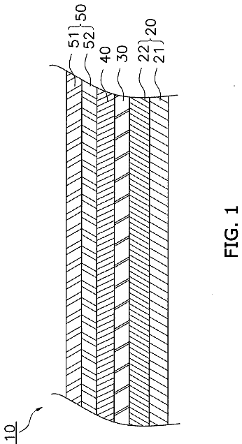
FIGS. 1A, 1B and 1C are schematic cross sectional views of the first embodiment of piezoelectric element according to the present invention, showing an exemplary configuration thereof.
FIGS. 2A, 2B and 2C are schematic cross sectional views of the first embodiment of piezoelectric element according to the present invention, showing another exemplary configuration thereof.
FIGS. 3A and 3B are a schematic cross sectional view and a schematic back surface view of a piezoelectric actuator according to the present invention, showing an exemplary configuration thereof.
FIGS. 4A and 4B are schematic views of a liquid ejection head and a liquid ejection device according to the present invention, respectively showing exemplary configurations thereof.
FIG. 5 is a schematic view of a vibration correction mechanism according to the present invention, showing an exemplary configuration thereof.
FIGS. 6A and 6B are schematic views of a variable optical component and a movable optical component according to the present invention, respectively showing exemplary configurations thereof.
FIGS. 7A, 7B and 7C are schematic views of an optical instrument according to the present invention, respectively showing exemplary configurations thereof.
FIG. 8 is a schematic view of an imaging device according to the present invention, showing an exemplary configuration thereof.
FIGS. 9A and 9B are schematic views of an optical switch according to the present invention, showing an exemplary configuration thereof.
FIG. 10 is a schematic view of a micromirror device according to the present invention, showing an exemplary configuration thereof;
FIGS. 11A and 11B are schematic views of an ultrasonic probe and an ultrasonic inspection device according to the present invention, respectively showing exemplary configurations thereof.
FIG. 12 is a schematic view of an acoustic component according to the present invention, showing an exemplary configuration thereof.
FIG. 13 is a schematic view of an angular velocity sensor according to the present invention, showing an exemplary configuration thereof.
FIG. 14 is a schematic view of a vibration power generation device according to the present invention, showing an exemplary configuration thereof.
FIGS. 15A, 15B, 15C and 15D are schematic views of the second embodiment of piezoelectric element according to the present invention, a surface acoustic wave generating device and a piezoelectric shutter according to the present invention, respectively showing exemplary configurations thereof.
FIGS. 16A and 16B are schematic illustrations of the content ratios of the ingredients of the piezoelectric film portions of the embodiments of piezoelectric element according to the present invention.
Description of the embodiments
Preferred embodiments of the present invention will now be described in detail in accordance with the accompanying drawings.
A piezoelectric element according to the present invention comprises a substrate, a first electrode, a piezoelectric film and a second electrode (first embodiment) or alternatively it comprises a substrate, a piezoelectric film and a plurality of comb-shaped electrodes (second embodiment).
The piezoelectric film is an oxide film containing Ba, Bi, Ti, Zr, Fe and Mn, wherein the value of y representing the molar ratio of Bi relative to the sum of Ba and Bi is 0.001≦y≦0.015; the value of x representing the molar ratio of Zr relative to the sum of Ti, Zr, Fe and Mn is 0.010≦x≦0.060; the value of z representing the molar ratio of Fe relative to the sum of Ti, Zr, Fe and Mn is 0.001≦z≦0.015; the value of m representing the molar ratio of Mn relative to the sum of Ti, Zr, Fe and Mn is 0.0020≦m≦0.0150; and the relationship between y and z is expressed by 0.90≦y/z≦1.10.
The general formula
as shown below is the chemical formula of the perovskite-type metal oxide, which is the principal ingredient of the piezoelectric film. (Ba.sub.1-yBi.sub.y)(Ti.sub.1-x-z-mZr.sub.zFe.sub.xMn.sub.m)O.sub.3 (1), where x, y, z, y/z and m are respectively defined as 0.010≦x≦0.060, 0.001≦y≦0.015, 0.001≦z≦0.015, 0.90≦y/z≦1.10 and 0.0020≦m≦0.0150.
(Configuration of Piezoelectric Element)
FIGS. 1A through 1C are schematic cross sectional views of the first embodiment of piezoelectric element according to the present invention, showing an exemplary configuration thereof. The first embodiment of piezoelectric element of the present invention has a configuration realized by arranging a substrate 101 , a first electrode 102 , a piezoelectric film 103 and a second electrode 104 . In the first embodiment shown in FIG. 1A , all of the first electrode 102 , the piezoelectric film 103 and the second electrode 104 have the same area and all the edge surfaces of them are vertically aligned in the direction perpendicular to the surface of the substrate 101 . However, the configuration of the first embodiment is by no means limited to the one illustrated in FIG. 1A . As seen from FIGS. 1B and 1C , each of the constituting parts may freely be modified in terms of area and shape according to the application thereof, or one or more than one additional constituting members may be arranged between them, so long as the arrangement of such additional members does not impair the function of the piezoelectric element as a whole. Examples of additional members that can be used for a piezoelectric element according to the present invention include one or more than one adhesion components 106 for enhancing the adhesiveness between the individual constituting parts and one or more than one buffer components for improving the crystallinity and the orientation of each of the constituting parts as shown in FIGS. 2A and 2B .
FIG. 15A is a schematic cross sectional view of the second embodiment of piezoelectric element according to the present invention, showing an exemplary configuration thereof. The second embodiment of piezoelectric element according to the present invention has a configuration realized by arranging a substrate 101 , a piezoelectric film 103 and a plurality of comb-shaped electrodes 105 . So long as the number of the comb-shaped electrodes 105 is not less than two, the arrangement of the comb-shaped electrodes 105 is not limited to the one illustrated in FIG. 15A , although it is preferable that the number of the electrodes is a multiple of two and the pair or each pair of them are interdigitally arranged as shown in FIG. 15A . The substrate 101 and the piezoelectric film 103 may or may not be patterned.
(Substrate)
While the material of the substrate 101 is not subjected to any limitations, it is preferably a material that is neither deformed nor molten in the heating process where the first electrode 102 , the piezoelectric film 103 and the second electrode 104 are arranged on the substrate. The highest temperature of the heating process is normally not higher than 800° C. Examples of preferable substrates that can be used for the purpose of the present invention include single crystal substrates of magnesium oxide (MgO), strontium titanate (SrTiO.sub.3), lanthanum aluminate (LaAlO.sub.3) and so on, ceramic substrates of zirconia (ZiO.sub.2), alumina (Al.sub.2O.sub.3), silica (SiO.sub.2) and so on, semiconductor substrates of silicon (Si), tungsten (W) and so on, and substrates of heat-resistant stainless steel (SUS). Two or more than two of such materials as listed above may be combined for use and two or more than two substrates may be laid one on the other to form a multilayered substrate structure.
When the piezoelectric film 103 is selectively oriented in the perpendicular direction relative to the surface of the substrate 101 , the underlying layers including the substrate 101 and the first electrode 102 are preferably oriented in a similar manner. If such is the case, a single crystal substrate is preferably employed for the substrate 101 .
(Electrodes)
As a piezoelectric element according to the present invention comprises a pair of electrodes, the piezoelectric film 103 can be made to produce piezoelectric strain by applying a voltage to the piezoelectric film 103 and an electric signal that corresponds to the strain of the piezoelectric film 103 can be drawn out. The material of the electrodes is not subjected to any particular limitations and any material that can normally be used for electrodes can also be used for the electrodes of a piezoelectric element according to the present invention. Examples of such materials include metals such as Ti, Pt, Ta, Ir, Sr, In, Sn, Au, Al, Fe, Cr, Ni, Pd, Ag, Cu and Ru and compounds of these metals. The use of metal electrodes of Ti, Pt, Au or Ru is particularly preferable.
The first electrode 102 , the second electrode 104 and the comb-shaped electrodes 105 may be made of a material selected from the above listed ones which may be formed as a laminated structure by laying two or more than two of those materials one on the other. Additionally, the first electrode 102 and the second electrode 104 may be made of respective materials that are different from each other.
The method of manufacturing the first electrode 102 , the second electrode 103 and the comb-shaped electrodes 105 is not subjected to any particular limitations, although an electrode thin film having a high density and an excellent electro-conductivity can be obtained by using a technique selected from sputtering, vapor deposition and CSD (chemical solution deposition). The electrodes may be patterned to make them show a desired shape.
The electrode width and the electrode pitch of the comb-shaped electrodes 105 are not subjected to any particular limitations and can be selected so as to match the properties of the surface acoustic waves to be oscillated by excitation. However, it is suited for excited oscillations of surface acoustic waves that both the electrode width and the electrode pitch are not less than 10 μm and not more than 500 μm.
(Piezoelectric Film)
For the purpose of the present invention, a piezoelectric film refers to a thin film-shaped crystal aggregate that shows a piezoelectric effect or an inverse piezoelectric effect. A thin film is a texture arranged so as to cover one or both of the surfaces of a flat-shaped base member (substrate) and to be brought into tight contact with the latter. As shown in FIG. 1A , an electrode layer such as a first electrode 102 or an adjustment layer may be arranged between the substrate 101 and the piezoelectric film 103 . The piezoelectric film 103 may directly cover the surface of the substrate 101 as shown in FIG. 15A . As far as the present invention is concerned, a film that has a film thickness, or the thickness that the film shows when it is measured in the direction perpendicular to the plane where it is arranged, of less than 10 μm and in which the number of crystal grains as counted in the above defined perpendicular direction is not more than 20 is referred to as thin film. A so-called piezoelectric ceramic product obtained by baking a metal oxide so as to produce a molded independent object differs from the piezoelectric film of a piezoelectric element according to the present invention and hence is not within the scope of the present invention.
Unlike a piezoelectric ceramic product that is independent from a substrate, the piezoelectric film is held in tight contact with the substrate and hence is bound by the substrate. Compressive stress or tensile stress arises in the inside of the piezoelectric film that is bound by the substrate in directions running along the film surface. Therefore, the piezoelectric film of a piezoelectric element according to the present invention has residual stress in a direction parallel with the surface of the substrate. This residual stress suppresses any change in the crystal structure of the piezoelectric film that arises in response to a change in the external environmental temperature. Then, as a result, the Curie temperature of the piezoelectric film becomes higher than a piezoelectric ceramic product having the same composition as that of the piezoelectric film and hence the actual operating temperature range is expanded toward the high temperature side.
Note that the internal residual stress of the piezoelectric film is generated along the surface thereof that is held in tight contact with the substrate and therefore the internal residual stress is reduced as the film thickness is increased. For example, when the thickness of the piezoelectric film is greater than 10 μm, any effect of raising the Curie temperature due to the internal residual stress can no longer be expected.
Adaptability to microprocessing is another advantage of a piezoelectric film over piezoelectric ceramic products. A piezoelectric film having a thickness less than 10 μm can be processed to make it show a micropattern by means of a patterning operation during the film forming process or by means of an etching operation after the film forming process.
(Perovskite-Type Metal Oxide)
For the purpose of the present invention, a perovskite-type metal oxide refers to a metal oxide having a perovskite structure, which is ideally a cubic crystal structure, as defined in Iwanami Dictionary of Physics and Chemistry, Ver. 5 (Iwanami Shoten Publishers, published on Feb. 20, 1998). Metal oxides having a perovskite structure are generally expressed by the chemical formula of ABO.sub.3. In a perovskite-type metal oxide, element A and element B take an ionic form and occupy specific respective positions in a unit lattice that are referred to respectively as A-site and B-site. For example, in the case of a unit lattice of a cubic crystal system, element A is located at the vertexes of the cube and element B is located at the body center of the cube. Element O takes the form of oxygen anion and is located at the face centers of the cube.
A metal oxide expressed by the general formula
means that the metal elements located at A-sites are Ba and Bi and metal elements located at B-sites are Ti, Zr and Fe. Note, however, that some of the elements Ba and Bi may be located at B-sites and, similarly, some of the elements Ti, Zr and Fe may be located at A-sites.
When the molar ratio of the elements at B-sites to the element O is 1:3 in a metal oxide expressed by the above describe general formula
and if the molar ratio is shifted slightly, for example by not less than 1%, such a shifted molar ratio is within the scope of the present invention provided that the metal oxide has a perovskite structure as its main phase.
When the molar ratio of the elements at A-sites to the elements at B-sites is 1:1 in the metal oxide expressed by the above describe general formula
and if the amount of the elements at A-sites shows a surplus or shortage of between −5% and 20%, such a surplus or shortage is within the scope of the present invention provided that the metal oxide has a perovskite structure as its main phase.
If the metal oxide has a perovskite structure or not can be determined by examining the piezoelectric film to see its X-ray diffraction or electron diffraction peaks. The piezoelectric film of a metal oxide having a perovskite structure as main crystal phase may auxiliary have some other crystal phases.
(Composition Ratio of Piezoelectric Film)
When the piezoelectric film of a piezoelectric element according to the present invention contains Bi and Fe within the range expressed in the general formula (1), the piezoelectric film shows an improved piezoelectric constant and a reduced dielectric loss (also referred to as dielectric tangent or tan δ) in the temperature range between −30° C. and 50° C., particularly in the low temperature range not higher than 20° C. Most of the trivalent Bi elements are located at A-sites of the perovskite skeleton while most of the trivalent Fe elements are located at B-sites. While Bi.sup.3+ ions can position themselves both at A-sites and B-sites, since Fe.sup.3+ ions having a relatively small ionic radius preferentially take positions at B-sites and the amount of Fe.sup.3+ ions is substantially equal to the amount of Bi.sup.3+ ions in a piezoelectric element according to the present invention, Bi.sup.3+ ions consequently take positions at A-sites.
As Bi.sup.3+ ions take positions at A-sites, the cubic crystal lattices become stabilized under the effect of the lone pairs of electrons that Bi.sup.3+ ions have. Then, as a result, the phase transfer temperature T.sub.to from tetragonal crystal to orthorhombic crystal in the crystal structure of the principal ingredients of the piezoelectric film is shifted toward the low temperature side. Due to this fact, the piezoelectric constant is improved and the dielectric loss is reduced between −30° C. and 50° C. (within the drive temperature range of piezoelectric element). Particularly in the low temperature range not higher than 20° C., a remarkable effect can be obtained because the orthorhombic crystal phase that appears when Bi and Fe are non-existent is turned into a tetragonal crystal phase due to the existence of Bi and Fe.
In the above-described general formula (1), the value of x that represents the molar ratio of Zr at B-sites is within the range of 0.010≦x≦0.060, preferably 0.030≦x≦0.060. When the value of x is greater than 0.060, the Curie temperature falls while the high temperature resistance becomes insufficient in any application of the piezoelectric film to a piezoelectric element and the dielectric loss increases at high temperatures around 50° C. When, on the other hand, the value of x is smaller than 0.010, no satisfactory piezoelectric constant can be obtained in the temperature range between −30° C. and 50° C. in any application of the piezoelectric film to a piezoelectric element.
In the above-described general formula (1), y that represents the molar ratio of Bi at A-sites and z that represents the molar ratio of Fe at B-sites are respectively within the temperature ranges of 0.001≦y≦0.015 and 0.001≦z≦0.015.
When the molar ratio of either Bi or Fe falls below 0.001, no satisfactory piezoelectric constant can be obtained within the temperature range between −30° C. and 50° C., particularly in the low temperature range not higher than 20° C., in any application of the piezoelectric film to a piezoelectric element. When, on the other hand, the molar ratio of either Bi or Fe exceeds 0.015, the dielectric loss is increased in the temperature range between −30° C. and 50° C. From the viewpoint of obtaining a preferable piezoelectric constant and a preferable dielectric loss, both the molar ratio of Bi and that of Fe (the y value and the z value) are preferably not less than 0.001 and not more than 0.010. More preferably, both the content ratio of Bi and that of Fe (the y value and the z value) are not less 0.002 and not more than 0.008.
In the above-described general formula (1), the ratio of y that represents the molar ratio of Bi at A-sites to z that represents the molar ratio of Fe at B-sites, or y/z, is within the range of 0.90≦y/z≦1.10 and ideally y/z=1. When y/z falls below 0.90, the piezoelectric constant is reduced because Fe precipitates onto grain boundaries and forms non-perovskite type auxiliary phases with other elements. When, on the other hand, y/z exceeds 1.10, the dielectric loss is increased because Bi oxide precipitates onto grain boundaries.
In the above-described general formula (1), m that represents the molar ratio of Mn at B-sites is not less than 0.0020 and not more than 0.0150.
When the piezoelectric film is made to contain Mn within the above defined range of content ratio, the piezoelectric constant of a piezoelectric element according to the present invention is found at an improved level and the dielectric loss is suppressed within the temperature range between −30° C. and 50° C. When the Mn molar ratio m is less than 0.0020, the physical properties of the piezoelectric film show little difference with those of piezoelectric film containing no Mn and hence the above-described advantages cannot satisfactorily be obtained. When, on the other hand, the Mn molar ratio m exceeds 0.0150, the dielectric loss of the piezoelectric element dramatically increases. When the dielectric loss of the piezoelectric element exceeds 1.5% (measurement frequency: 1 kHz) within the temperature range between −30° C. and 50° C., there arise problems such as heat generation that takes place while the piezoelectric element is in operation and a remarkable increase of power consumption.
The Mn contained in the piezoelectric film is not limited to metal Mn. In other words, it is sufficient for the piezoelectric film to contain Mn as ingredient. For example, Mn may exist as solid solution at B-sites or may be contained at grain boundaries. Furthermore, Mn ingredient may be contained in the piezoelectric film in the form of metal, ion, oxide, metal salt or complex. Generally, Mn can take a valence of 4+, 2+ or 3+.
The means of observing the composition of a piezoelectric film according to the present invention is not subjected to any particular limitations. Means that can be used for observing the composition include X-ray fluorometry (XRF), inductively coupled plasma atomic emission spectrometry (ICP-AES) and atomic absorption spectrometry (AAS). With any of these means, the weight ratio and the composition ratio of each of the elements contained in the piezoelectric film can be determined. Of the above-listed means, the particularly preferable one for determining the composition is XRF.
(Other Ingredients of Piezoelectric Film)
The above-described piezoelectric film may contain Ca and Sr to such an extent that commercially available materials of Ba inevitably contain, Nb to such an extent that commercially available materials of Ti inevitably contain, and Hf to such an extent that commercially available materials of Zr inevitably contain.
For the purpose of the present invention, the expression that the principal ingredients of a piezoelectric film are Ba, Bi, Ti, Zr, Fe, Mn and O means that, when the composition of the piezoelectric film is analyzed, the top seven elements in terms of abundance ratios expressed by molar quantities (numbers of atoms) are Ba, Bi, Ti, Zr, Fe, Mn and O. The piezoelectric film preferably contains Ba, Bi, Ti, Zr, Fe, Mn and O (the perovskite-type metal oxide as expressed by the general formula (1)) by not less than 98.5 mol % as sum total.
(Thickness of Piezoelectric Film)
Preferably, the maximum thickness T.sub.P of the piezoelectric film 103 in the region thereof that is sandwiched between the first electrode 102 and the second electrode 104 is not more than 10 μm. When the film is not flat, the film thickness is measured in the direction perpendicular to the surface of the substrate 101 , using the surface of the substrate 101 as starting point. The preferable upper limit of the maximum film thickness T.sub.P is 5,000 nm, while the lower limit thereof is 500 nm. By defining the maximum film thickness T.sub.P to be not less than 500 nm and not more than 5,000 nm, the obtained piezoelectric film functions well and the processability of the piezoelectric film for forming an element can be secured.
More preferably, the maximum film thickness T.sub.P of the piezoelectric film 103 is not less than 700 nm and not more than 4,000 nm. Most preferably, it is not less than 1,000 nm and not more than 3,500 nm.
The maximum film thickness T.sub.P of the piezoelectric film 103 can be measured by means of a contact step meter or by microscopic observation of a cross section of the film.
FIG. 1C shows an exemplar maximum film thickness T.sub.P identified for a piezoelectric element according to the present invention and having a patterned piezoelectric film 103 .
(Thickness of Electrodes)
The average value of the maximum film thickness T.sub.E1 and the minimum film thickness T.sub.E2 of the first electrode 102 and the second electrode 104 , or (T.sub.E1+T.sub.E2)/2, is preferably within the range of 0.002×T.sub.P≦(T.sub.E1+T.sub.E2)/2≦500 nm. The maximum film thickness T.sub.E1 and the minimum film thickness T.sub.E2 are determined in the region where the first electrode 102 and the second electrode 104 are disposed oppositely relative to each other with the piezoelectric film sandwiched between them. In other words, if either or both of the electrodes have a dummy portion that does not participate in the function of the piezoelectric element, the film thickness of such a dummy portion is not taken into consideration. The maximum film thickness of the first electrode 102 and the maximum film thickness of the second electrode 104 are compared and the greater one is selected and specified as T.sub.E1. Similarly, the minimum film thickness of the first electrode 102 and the minimum film thickness of the second electrode 104 are compared and the smaller one is selected and specified as T.sub.E2. The maximum film thickness and the minimum film thickness of each of the electrodes can be measured by microscopic observation of a cross section of the electrode.
FIG. 1C shows an example where the maximum film thickness and the minimum film thickness of the second electrode 104 , which is a patterned electrode, of a piezoelectric element according to the present invention are selected and specified respectively as T.sub.E1 and T.sub.E2. In this instance, the first electrode 102 is made of a flat film and has a uniform film thickness that is found somewhere between T.sub.E1 and T.sub.E2.
The lower limit of the average value (T.sub.E1+T.sub.E2)/2 is 0.002×T.sub.P, which is 0.2% of the maximum film thickness T.sub.P of the piezoelectric film 103 . For example, when T.sub.P=5,000 nm, the lower limit of (T.sub.E1+T.sub.E2)/2 is 10 nm. As far as this requirement is satisfied, the electric resistance of each of the electrodes shows a large and uniform value and does not vary as a function of the point on it so that consequently a much more uniform voltage is applied to the piezoelectric element to realize a preferable result.
The upper limit of the average value (T.sub.E1+T.sub.E2)/2 is 500 nm. As far as this requirement is satisfied, the risk that the electrodes can obstruct the operation of detecting the strain generated in the piezoelectric element is reduced to realize a preferable result.
For the second embodiment of piezoelectric element according to the present invention, the average value of the maximum film thickness T.sub.E1 and the minimum film thickness T.sub.E2 of the comb-shaped electrodes, or (T.sub.E1+T.sub.E2)/2, is preferably within the range of 0.002×T.sub.P≦(T.sub.E1+T.sub.E2)/2≦500 nm.
(Adhesion Component)
An adhesion component containing a metal of Group IV elements and/or a metal of Group V elements is preferably interposed between the first electrode and the substrate. FIGS. 2A and 2B are schematic cross sectional views of an embodiment of piezoelectric element according to the present invention in which an adhesion component 106 is arranged between the substrate 101 and the first electrode 102 . The adhesion component may be arranged as a number of spot-like pieces that are embedded in the first electrode as in the case of the adhesion component 106 shown in FIG. 2A or as a layer having a thickness of not less than 1 nm and not more than 10 nm as in the case of the adhesion component 106 shown in FIG. 2B . The material of the adhesion component 106 is preferably selected from free metals of Ti, Zr and Hf of Group IV elements, oxides thereof and nitrides thereof and/or from free metals of V, Nb and Ta of Group V elements, oxides thereof and nitrides thereof from the viewpoint of adhesiveness. All or part of the adhesion component 106 may be chemically bonded to the substrates 101 or the first electrode 102 to form an alloy or a composite oxide.
(Crystal Structure of Piezoelectric Film)
For the purpose of the present invention, a piezoelectric film refers to a thin film-shaped crystal aggregate and, preferably, the crystal aggregate has a texture formed of crystal grains having a columnar structure. FIG. 2C is a schematic cross sectional view of a piezoelectric element having a piezoelectric film 103 that has a texture produced by crystal grains having a columnar structure in the inside thereof. In FIG. 2C , both the shaded regions and the unshaded regions indicate crystal grains having a columnar structure. The fact that the crystal grains have a columnar structure can be confirmed by observing a cross section of the piezoelectric film portion of the piezoelectric element by means of a microscope. In most instances, a crystal grain having a columnar structure and a crystal grain located adjacent to the former one show different crystal orientations and hence the grain boundaries can be determined by seeing the light areas and shaded areas in the microscopic image. A texture refers to a state where two or more than two crystal grains are located adjacent to each other and, preferably, substantially all the area of a cross section of the piezoelectric film 103 shows an aggregate of columnar crystals. Ideally, a single crystal grain having a columnar structure is held in contact with both the first electrode 102 and the second electrode 104 . In the instance of the second embodiment of piezoelectric element according to the present invention, a single crystal grain is preferably held in contact with both the substrate 101 and one of the comb-shaped electrodes 105 .
The crystal grain diameter of the piezoelectric film 103 at the film surface is preferably not less than 300 nm and not more than 5,000 nm in terms of average circle equivalent diameter. If this requirement is satisfied, the piezoelectric constant of the piezoelectric element becomes more satisfactory in the temperature range between −30° C. and 50° C. In addition, if the crystal grain diameter is not greater than 5,000 nm, the thin film piezoelectric element shows an excellent processability. The expression of “circle equivalent diameter” refers to the expression of “projected area equivalent circle diameter” that is being popularly used in the field of microscopic observations and means the diameter of a real circle having the same area as the projected area of the crystal grain that is the target of microscopic observation. For the purpose of the present invention, the method of measuring the circle equivalent diameter is not subjected to any particular limitations. For example, the circle equivalent diameter can be determined by processing a photographic image obtained by observing the surface of the piezoelectric material that is the target of observation by means of a polarization microscope or a scanning electron microscope. Because the optimum magnification of microscope may vary as a function of the grain diameter to be observed, an optical microscope and an electron microscope may selectively be employed for the observation. The circle equivalent diameter may be determined not from the surface of the material but from an image of the polished surface or of a cross section. The expression of “average circle equivalent diameter” refers to the average value of the circle equivalent diameters of a plurality of crystal grains.
(Curie Temperature)
The Curie temperature of the piezoelectric film of a piezoelectric element according to the present invention is preferably not lower than 121° C. When the Curie temperature of the piezoelectric film is not less than 121° C., the Curie temperature can be considered as being sufficiently separated from the drive temperature range (between −30° C. and 50° C.) of the piezoelectric element. Such a Curie temperature is preferable, because in that case, even if an abrupt temperature change takes place at and near such a Curie temperature, the influence of the Curie temperature change on the piezoelectric constant and the dielectric loss of the piezoelectric element can be disregarded in the drive temperature range of the piezoelectric element. More preferable Curie temperature range is not lower than 130° C. and not higher than 195° C.
The description continues in the full USPTO document.
 Lapsed, fee not paid2 drawings