 Lapsed, fee not paid6 drawings
Hardware & Electronics · US 9,886,889 B2
Shift register unit, gate driving circuit and display device
There provide a shift register unit, a gate driving circuit and a display device.
US 9,886,921 B2 · Assignee: BEIJING BOE OPTOELECTRONICS TECHNOLOGY CO., LTD. · Inventors: Chen; Xiaochuan et al.
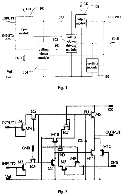
Sheet 1 of 3 from the published document. All sheets in the USPTO PDF
A gate driving circuit comprises GOA units of multiple stages. Each GOA unit includes a pull-up module and an output module. The pull-up module outputs a second clock signal to the output module when an input signal is at a high level; and the output module is turned on when the second clock signal is at a high level, and outputs a third clock signal as a first gate driving signal and outputs a fourth clock signal as a second gate driving signal when being turned on; the third clock signal and the fourth clock signal have opposite phases but the same cycle, and the cycle of the second clock signal is twice that of the third clock signal. It also discloses a liquid crystal display and a gate driving method, two rows of pixels are driven by one GOA unit, thus the space for disposing TFTs is saved, the sealing area of the LCD is reduced.
At present, LCDs are commonly used flat panel displays, wherein Thin Film Transistor Liquid Crystal Display (TFT-LCD) is the mainstream product. With the increasingly fierce competition of TFT-LCD products, manufacturers have to reduce costs of products by means of adopting new technologies one after another, so as to enhance market competitiveness of products. The Gate on Array (GOA) technology refers to integrating gate drivers of the TFT-LCD on an array substrate, thus forming scan driving to the panel. As compared with the conventional techniques of Chip On Flex/Film (COF) and Chip On Glass (COG), the GOA technology not only can save costs, but also can achieve symmetry on both sides of the panel, which beautifies the design and leaves out a bonding area and a fan-out wiring space of the gate integrated circuit (Gate IC), thus achieving the design of a narrow frame; meanwhile, since
1 of 3 drawing sheets so far from the published document, cropped to the drawing. Every sheet is in the USPTO PDF.
What the patent claimed, word for word. All of it is now free to use.
The present disclosure relates to the technology of gate driving, and in particular to a gate driving circuit, a gate driving method, and a liquid crystal display (LCD).
At present, LCDs are commonly used flat panel displays, wherein Thin Film Transistor Liquid Crystal Display (TFT-LCD) is the mainstream product. With the increasingly fierce competition of TFT-LCD products, manufacturers have to reduce costs of products by means of adopting new technologies one after another, so as to enhance market competitiveness of products. The Gate on Array (GOA) technology refers to integrating gate drivers of the TFT-LCD on an array substrate, thus forming scan driving to the panel. As compared with the conventional techniques of Chip On Flex/Film (COF) and Chip On Glass (COG), the GOA technology not only can save costs, but also can achieve symmetry on both sides of the panel, which beautifies the design and leaves out a bonding area and a fan-out wiring space of the gate integrated circuit (Gate IC), thus achieving the design of a narrow frame; meanwhile, since the technique of gate direction bonding can be saved, it also facilitates improving productivity and yield.
Currently, the GOA circuit commonly used in the gate driving circuit adopts a 10T1C mode, in which one GOA unit in the gate driving circuit can drive only one row of gates and ten TFTs are needed to drive each row of gates. However, a display device with a small size will have an extremely small dot pitch under a resolution with a high number of Pixel Per Inch (PPI), less than 30*90 μm sometimes, if ten TFTs are disposed on a space of 90 μm, these ten TFTs need to be arranged in a row, in this way, a quite large sealing area is required.
In view of the above, a primary object of the present disclosure is to provide a gate driving circuit, a gate driving method, and a display that can reduce the space occupied by the GOA circuit, and thereby reduce the sealing area of the display device.
To achieve the above object, the technical solutions of the present disclosure are implemented as follows:
The present disclosure provides a gate driving circuit comprising GOA units of multiple stages, each of the GOA units including a pull-up module and an output module,
the pull-up module for outputting a second clock signal to the output module when an input signal is at a high level; and
the output module for being turned on when the second clock signal is at a high level, and outputting a third clock signal as a first gate driving signal and outputting a fourth clock signal as a second gate driving signal when being turned on,
wherein the third clock signal and the fourth clock signal have opposite phases but the same cycle, the cycle of the second clock signal is twice that of the third clock signal.
In the above technical solution, the GOA unit further comprises a pull-down module for pulling down voltage of the pull-up module.
In the above technical solution, when the second clock signal changes from a low level to a high level, the third clock signal changes from a low level to a high level and the fourth clock signal changes from a high level to a low level.
In the above technical solution, the pull-up module comprises a first switching device, a boosting device, and a third switching device, wherein the source of the first switching device is taken as an input signal terminal, the gate of the first switching device is connected to the source thereof, and the drain of the first switching device is connected to one end of the boosting device; the other end of the boosting device is connected to the drain of the third switching device; the gate of the third switching device is connected to a connection point of the drain of the first switching device and the boosting device, the source of the third switching device is taken as a second clock signal input terminal, the drain of the third switching device is connected to the other end of the boosting device; and
a connection point of the boosting device and the drain of the third switching device is taken as an output terminal of the pull-up module, and connected to the output module.
In the above technical solution, the output module comprises a seventh switching device and a tenth switching device; wherein the gate of the seventh switching device is connected to the output terminal of the pull-up module, the source of the seventh switching device is taken as a third clock signal input terminal, and the drain of the seventh switching device is taken as a first gate driving signal output terminal; the gate of the tenth switching device is connected to the output terminal of the pull-up module, the source of the tenth switching device is taken as a fourth clock signal input terminal, and the drain of the tenth switching device is taken as a second gate driving signal output terminal.
In the above technical solution, the output module is further for pulling down the first gate driving signal when the third clock signal changes from a low level to a high level and the fourth clock signal changes from a high level to a low level.
In the above technical solution, the output module further comprises an eleventh switching device, the gate of the eleventh switching device is connected to the fourth clock signal input terminal, the source of the eleventh switching device is connected to the first gate driving signal output terminal, and the drain of the eleventh switching device is connected to a low level terminal.
In the above technical solution, the second clock signals of adjacent GOA units have opposite phases but the same cycle.
The present disclosure also provides a liquid crystal display, comprising the gate driving circuit described above.
The present disclosure also provides a gate driving method, the method comprising:
outputting, by a pull-up module, a second clock signal to an output module when an input signal is at a high level; and
turning on the output module when the second clock signal is at a high level, so as to output a third clock signal as a first gate driving signal and output a fourth clock signal as a second gate driving signal,
wherein the third clock signal and the fourth clock have opposite phases but the same cycle, and the cycle of the second clock signal is twice that of the third clock signal.
In the above technical solution, when the second clock signal changes from a low level to a high level, the third clock signal changes from a low level to a high level and the fourth clock signal changes from a high level to a low level.
In the above technical solution, after outputting the third clock signal as the first gate driving signal and prior to outputting the fourth clock signal as the second gate driving signal, the method further comprises pulling down, by the output module, the first gate driving signal when the third clock signal changes from a low level to a high level and the fourth clock signal changes from a high level to a low level.
One GOA unit in the gate driving circuit of the present disclosure can output two gate driving signals, thus, two rows of pixels are driven by one GOA unit, as compared with the conventional GOA circuit, less TFTs are required to drive two rows of pixels, thus the space for disposing TFTs is saved, the sealing area of the LCD is reduced, and the narrow frame of the LCD is achieved.
FIG. 1 is a schematic diagram of functional configuration of each GOA unit in a gate driving circuit of the present disclosure;
FIG. 2 is a schematic diagram of architecture of specific components of a GOA unit in a gate driving circuit of a first embodiment of the present invention;
FIG. 3 is a time sequence diagram of input and output signals of a GOA unit in a gate driving circuit of the first embodiment of the present invention;
FIG. 4 is a flow chart of implementation of a gate driving method in a second embodiment of the present invention;
FIG. 5 is a schematic diagram of architecture of specific components of a GOA unit in a gate driving circuit of a third embodiment of the present invention; and
FIG. 6 is a schematic diagram of architecture of specific components of a GOA unit in a gate driving circuit of a fourth embodiment of the present invention.
With respect to the LCD of the present disclosure, its array substrate comprises p (p is an integer not less than one) data driving lines and q (q is an integer not less than one) gate driving lines, pixels are set on areas where the data driving lines and the gate driving lines are interleaved, that is to say, pixels of p rows and q columns are set on the array substrate of the LCD, a gate driving circuit of the LCD outputs a gate driving signal to the pixels through the gate driving lines, and thereby drives the pixels to open, so that the respective pixels can receive a data signal output by the data driving circuit through the data driving lines, and thereby an image is displayed based on the data signal.
The gate driving circuit of the LCD comprises GOA units of multiple stages, each GOA unit can drive two adjacent rows of pixels, to be specific, the GOA unit of each stage drives two adjacent rows of pixels through two gate driving lines, when the GOA unit outputs a signal at a high level, the corresponding two adjacent rows of pixels are driven to be opened through the corresponding gate driving lines, so that the corresponding two adjacent rows of pixels can receive a data signal; when the GOA unit outputs a signal at a low level, the corresponding two adjacent rows of pixels are closed to stop receiving the data signal. Thus, in one frame of picture, the GOA units of multiple stages in the gate driving circuit output a signal at a high level in sequence, and drive the pixels one by one with two adjacent rows of pixels as a unit.
Each GOA unit has an input signal terminal (INPUT terminal), a reset signal input terminal (RESET input terminal), a low level (VSS) terminal, a first clock signal (CLK 1 ) input terminal, a second clock signal (CLK 2 ) input terminal, a third clock signal (CLK 3 ) input terminal, a fourth clock signal (CLK 4 ) input terminal, a first gate driving signal (OUTPUT_n) output terminal, and a second gate driving signal (OUTPUT_n+1) output terminal, wherein OUTPUT_n is a gate driving signal for the n-th row of pixels, OUTPUT_n+1 is a gate driving signal for the n+1-th row of pixels (n is an integer not less than 1, n is not less than the total number p of rows of pixels, if n is the last row of pixels, then the OUTPUT_n+1 terminal can be useless). The GOA unit of any stage other than the first stage takes an output signal OUTPUT_n−1 of a GOA unit of a previous stage as INPUT, and takes an output signal OUTPUT_n+2 of a GOA unit of a next stage as RESET; in particular, as for the GOA unit of the first stage, it takes an STV signal (frame opening signal) as INPUT, as for the GOA unit of the last stage, usually a dummy GOA unit that is resultant and useless is designed to reset it.
Specifically, as shown in FIG. 1 , the GOA unit of each stage comprises a pull-up module 11 and an output module 12 . The pull-up module 11 outputs CLK 2 to the output module 12 when INPUT is at a high level, the output module 12 is tuned on when CLK 2 is at a high level, and outputs CLK 3 as the first gate driving signal (OUTPUT_n), and outputs CLK 4 as the second gate driving signal (OUTPUT_n+1) when being turned on, wherein CLK 3 and CLK 4 have opposite phases but the same cycle.
In addition, the pull-up module 11 is further for, when RESET is at a high level, stopping outputting CLK 2 to the output module 12 , so that the output module 12 is able to quickly stop outputting the gate driving signal and complete a reset operation. Thus it can be known that, the output module 12 , under the action of the pull-up module 11 , can implement normally outputting and completing a shift within one cycle, and also can make the GOA unit reset according to the RESET signal and complete a reset operation in the operating process of the GOA unit.
The GOA unit of each stage further comprises a pull-down module 13 for pulling down voltage of the pull-up module 11 , i.e., suppressing noise of the pull-up module 11 . First Embodiment
In this embodiment, the specific circuit structure of GOA unit of each stage is shown in FIG. 2 , wherein the pull-up module 11 comprises a first switching device M 1 , a second switching device M 2 , a boosting device C 1 , and a third switching device M 3 , the source of M 1 is taken as the INPUT terminal, the gate of M 1 is connected to the source thereof, and the drain of M 1 is connected to the source of M 2 , a connection point of the drain of M 1 and the source of M 2 is a pull up (PU) point, the drain of M 2 is connected to a low level (VSS) terminal, the gate of M 2 is connected to the RESET terminal, one end of the boosting device C 1 is connected to the gate of M 3 and to the PU point, the other end of C 1 is connected to the drain of M 3 and taken as an output terminal of the pull-up module 11 , the source of M 3 is taken as the second clock signal input terminal.
The output module 12 comprises a seventh switching device M 7 , an eleventh switching device M 11 , and a tenth switching device M 10 , wherein the gate of M 7 is connected to the output terminal of the pull-up module 11 , i.e., being connected to a connection point of C 1 and the drain of M 3 , the source of M 7 is taken as the CLK 3 input terminal, and the drain of M 7 is taken as the OUTPUT_n output terminal; the gate of M 10 is connected to the output terminal of the pull-up module 11 , i.e., being connected to a connection point of C 1 and the drain of M 3 , the source of M 10 is taken as the fourth clock signal input terminal, the drain of M 10 is taken as the OUTPUT_n+1 output terminal; the source of M 11 is connected to the drain of M 7 , i.e., being connected to the OUTPUT_n output terminal, the gate of M 11 is connected to the source of M 10 , i.e., being connected to the CLK 4 input terminal, and the drain of M 11 is connected to the VSS terminal.
The pull-down module 13 comprises a fourth switching device M 4 , the gate of M 4 is connected to the RESET terminal, and the drain of M 4 is connected to the drain of M 3 , i.e., the output terminal of the pull-up module 11 , the source of M 4 is connected to the VSS terminal. Voltage at the output terminal of the pull-up module 11 is pulled down according to the RESET signal.
The pull-down module 13 may further comprise a fifth switching device M 5 , a sixth switching device M 6 , an eighth switching device M 8 , a ninth switching device M 9 , and a twelfth switching device M 12 , wherein the source of M 9 is taken as the CLK 1 input terminal, the gate of M 9 is connected to the source thereof, the drain of M 9 is connected to the source of M 8 and the gate of M 5 , this connection point is a pull down (PD) point; the gate of M 8 is connected to the gate of M 6 and to the PU point, the drain of M 8 and the drain of M 6 are connected to the VSS terminal, the source of M 6 is connected to the drain of M 5 , and the source of MS is connected to the source of M 9 .
The source of M 12 is connected to the PU point, the gate of M 12 is connected to the PD point of the pull-down module, and the drain of M 2 and the drain of M 12 are connected to the low level (VSS) terminal.
The operating process of the GOA unit described above is as follows: when the gate driving signal output by the GOA unit of a previous stage is OUTPUT_n−1, that is, INPUT of the GOA unit of the current stage is at a high level, M 1 is turned on to charge the PU point, C 1 further pulls up the voltage at the PU point, i.e., charging the gate of M 3 , M 3 is turned on; thereafter, CLK 2 changes from a low level to a high level, since M 3 is turned on, a high level signal of CLK 2 is transmitted to the gate of M 7 and the gate of M 10 to make M 7 and M 10 be turned on, CLK 3 is also at a high level, then the drain of M 7 , i.e., the OUTPUT_n output terminal, outputs CLK 3 at a high level, that is, it outputs OUTPUT_n to drive the n-th row of pixels to open; thereafter. CLK 3 changes from a high level to a low level, the OUTPUT_n output terminal stops outputting OUTPUT_n, CKL 4 changes from a low level to a high level, since M 10 is still in a turned-on state, the drain of M 10 , i.e., the OUTPUT_n+1 output terminal, outputs CKL 4 at a high level, that is, it outputs OUTPUT_n+1 to drive the n+1-th row of pixels to open, M 11 also is turned on to further pull down the OUTPUT_n output terminal, make the OUTPUT_n output terminal output terminal stop outputting OUTPUT_n, and thereby suppress the noise generated at the OUTPUT_n output terminal in this process. When CLK 3 changes from a low level to a high level again and CLK 4 changes from a high level to a low level, CLK 2 changes from a high level to a low level, M 7 and M 10 are turned off, the OUTPUT_n output terminal and the OUTPUT_n+1 output terminal are quickly pulled down to stop outputting.
When the GOA unit of a next stage outputs OUTPUT_n+2, that is, the RESET of the GOA unit of the current stage is at a high level, M 2 is turned on to discharge the PU point, and pull down the voltage at the PU point, so that the voltage at the gate of M 3 is pulled down, M 3 is turned off, CLK 2 cannot be transmitted to the gate of M 7 and the gate of M 10 , which makes M 7 and M 10 remain in a turned-off state, the OUTPUT_n output terminal and the OUTPUT_n+1 output terminal of the GOA unit of the current stage stop outputting.
In the above process, when CLK 2 changes from a high level to a low level, CLK 1 changes from a low level to a high level, M 9 is turned on to charge the PD point, the voltage at the PD point is pulled up, M 5 is tuned on to charge the PD point to further pull up the voltage at the PD point, which makes M 12 and M 4 be turned on. M 12 discharges the PU point when being turned on, and suppresses the noise generated by the pull-up module 11 . M 4 discharges the other end of C 1 , the drain of M 3 , the gate of M 7 , and the gate of M 10 when being turned on, and suppresses the noise generated by the output module 12 . When CLK 2 is at a high level, that is, when the GOA unit of the current stage outputs normally, M 6 and M 8 are also turned on to suppress the noise generated by the pull-up module 11 .
The time sequence of input and output signals of the GOA unit as described above is as shown in FIG. 3 , wherein CLK 1 and CLK 2 are two clock signals having opposite phases but the same cycle, CLK 3 and CLK 4 are two clock signals having opposite phases but the same cycle, the cycle of CLK 2 is twice that of CLK 3 , the cycle of CLK 4 and CLK 3 is the time for which one row of pixels are opened, that is, 1/p of one frame of image, wherein p is the total number of rows of pixels. When CLK 2 changes from a low level to a high level, CLK 3 changes from a low level to a high level and CLK 4 changes from a high level to a low level. In particular, CLK 2 of the GOA unit of the current stage is the same as CLK 1 of the GOA unit of an adjacent stage, CLK 2 of the GOA unit of an adjacent stage is the same as CLK 1 of the GOA unit of the current stage. That is, the adjacent GOA units are opposite in phase but the same in cycle in terms of CLK 1 or CLK 2 .
From the above description with respect to the operating process, it can be known that, the function of C 1 in the pull-up module 11 is, when CLK 2 is at a high level, further pulling up the voltage at the PU point, and thereby reducing noise which is coupled to the PU point by CLK 2 via a parasitic capacitor of M 3 , that is, the noise of the output module 11 will be reduced accordingly. M 2 has a function similar to that of M 12 , it can pull down the voltage at the PU point when RESET is at a high level.
The pull-down module 13 is also optional. M 6 , M 8 , M 5 , and M 9 are for controlling the voltage at PD point, the voltage at the PD point controls the turning-on of M 12 , which further controls to pull down the voltage at the PU point, and thereby accelerates the turning-off of M 3 , so that the CLK 2 high level signal is not output to the output module 12 . As will be appreciated that, the voltage at the PD point may be controlled by using other ways, M 12 may be also controlled by a separate signal line, as long as the function of pulling down the voltage at the PU point by M 12 in this embodiment can be achieved. Meanwhile, the voltage at the PD point also controls the turning-on of M 4 , which can pull down the voltage input by the pull-up module 11 to the output module 12 , and pull down the voltage at the pull-up module 11 , that is, it can be also considered as suppressing noise of the output module 12 . Of course, M 4 in this embodiment may also be controlled to be turned on by the RESET signal. Through the above analysis it can be known that, the pull-down module 13 can be divided into three shunts, that is, a first pull-down shunt M 6 , M 8 , M 5 , M 9 and M 12 , a second pull-down shunt M 6 , M 8 , M 5 , M 9 and M 4 , and a third pull-down shunt M 4 (whose gate is connected to RESET), these three shunts may exist separately or in combination.
M 11 is also optional in the output module 12 . The function of M 11 is, under the action of CLK 4 , further pulling down the OUTPUT_n output terminal, making the OUTPUT_n output terminal stop outputting OUTPUT_n, and thereby suppressing the noise generated by the OUTPUT_n output terminal in this process.
The above M 1 to M 12 may specifically be Metal-Oxide-Semiconductor Field Effect Transistors (MOSFET). C 1 is a capacitor device. Since the manufacturing techniques of a source and a drain of the transistors are the same, the names of the source and the drain are interchangeable, and name change can be made according to the direction of the voltage. Second Embodiment
This embodiment provides a gate driving method, as shown in FIG. 4 , the method may mainly comprise the following steps:
Step 401 : outputting, by a pull-up module, a second clock signal to an output module when an input signal is at a high level;
Step 402 : turning on the output module when the second clock signal is at a high level, so as to output a third clock signal as a first gate driving signal and output a fourth clock signal as a second gate driving signal.
Herein, the third clock signal and the fourth clock signal have opposite phases but the same cycle, the cycle of the second clock signal is twice that of the third clock signal. In particular, when the second clock signal changes from a low level to a high level, the third clock signal changes from a low level to a high level and the fourth clock signal changes from a high level to a low level.
In the above method, after outputting the third clock signal as the first gate driving signal and prior to outputting the fourth clock signal as the second gate driving signal, the method may further comprise pulling down, by the output module, the first gate driving signal when the third clock signal changes from a low level to a high level and the fourth clock signal changes from a high level to a low level. Third Embodiment
In this embodiment, the specific circuit structure of GOA unit of each stage is shown in FIG. 5 , its architecture is substantially the same as that in the second embodiment, the difference lies in that a thirteenth switching device M 13 is added, the gate of M 13 is connected to the PD point, the source of M 13 is connected to the output terminal of the pull-up module 11 , i.e., being connected to a connection point of C 1 and the drain of M 3 , and the drain of M 13 is connected to the VSS terminal; the gate of M 4 is connected to the RESET input terminal, the source of M 4 is connected to the output of the pull-up module 11 , i.e., being connected to a connection point of C 1 and the drain of M 3 , the drain of M 4 is connected to the VSS terminal; M 4 at this time is controlled separately by the RESET signal, M 13 is controlled separately by a voltage signal at the PD point. In this way, M 13 pulls down the pull-up module under the control of the PD point, and M 4 pulls down the pull-up module under the control of the RESET, which makes M 4 and M 13 in common accomplish the function of M 4 in the first embodiment, that is, M 4 in the first embodiment does not need to be always in an operating status, which facilitates extending a service life. Fourth Embodiment
In this embodiment, the specific circuit structure of GOA unit of each stage is shown in FIG. 6 , its architecture is substantially the same as the GOA unit in the third embodiment, the difference lies in that a fourteenth switching device M 14 is added additionally in the pull-down module, the gate of M 14 is connected to the CLK 1 input terminal, the source of M 14 is connected to the output terminal of the pull-up module 11 , that is, being connected to a connection point of C 1 and the drain of M 3 , and the drain of M 14 is connected to the VSS terminal, in this way, when CLK 1 is at a high level, M 14 can further pull down the pull-up module, and thereby further improve the noise elimination capability of the GOA unit.
In the prior art, one GOA unit can drive only one row of pixels, the space required to dispose TFT is relatively large; while in the gate driving circuit of the present disclosure, one GOA unit can drive two rows of pixels, which is implemented requiring less TFTs as compared with the prior art, thus the space for disposing TFTs is saved, the sealing area is reduced, and the narrow frame of the LCD is achieved.
The above described are merely preferred embodiments of the present invention, they are not intended to limit the scope of the present invention.
Explanation of Reference signs: M 1 , a first TFT switching device; M 2 , a second TFT switching device; M 3 , a third TFT switching device; M 4 , a fourth TFT switching device; M 5 , a fifth TFT switching device; M 6 , a sixth TFT switching device; M 7 , a seventh TFT switching device; M 8 , an eighth TFT switching device; M 9 , a ninth TFT switching device; M 10 , a tenth TFT switching device; M 11 , an eleventh TFT switching device; M 12 , a twelfth TFT switching device; M 13 , a thirteenth TFT switching device; M 14 , a fourteenth TFT switching device; C 1 , a boosting device; 11 , a pull-up module; 12 , an output module; and 13 , a pull-down module.
About 5,129 words. The USPTO PDF has it with every drawing.
Fees are due 3.5, 7.5 and 11.5 years after grant. This patent expired on February 6, 2026, so the fee marked "not paid" was the one that went unpaid.
GATE DRIVING CIRCUIT, GATE DRIVING METHOD, AND LIQUID CRYSTAL DISPLAY
Filed Nov 2012 · published Jun 2014Gate driving circuit, gate driving method, and liquid crystal display
Filed Nov 2012 · granted Feb 2018Earlier publications, parents and continuations. None of them can still be enforced, or this patent would not be listed.
Prior art cited by the examiner or applicant. Useful when you check your own idea for novelty.
Everything on this page comes from the documents linked above.


