Lapsed, fee not paid7 drawings
Cameras, Displays & Optics · US 9,883,107 B2
Imaging apparatus
An imaging apparatus includes a shake correction unit, a pixel shift unit, and a controller.
US 9,883,123 B2 · Assignee: OLYMPUS CORPORATION · Inventors: Tanaka; Yoshinobu et al.
Sheet 1 of 8 from the published document. All sheets in the USPTO PDF
A solid-state imaging device includes a pixel signal processing unit which has a plurality of pixels disposed in a two-dimensional matrix, outputs each of pixel signals generated by all pixels as a total pixel signal, and outputs each of the pixel signals generated by the pixels with the number of pixels reduced to a prescribed number of pixels as a reduced pixel signal, a bit reduction method determination unit which determines a bit reduction method for reducing the number of pixels of a digital value representing the amount of the total pixel signal based on the reduced pixel signal, and a bit reduction unit which reduces the number of bits of the digital value based on the bit reduction method and outputs the digital value with the reduced number of bits as a digital value corresponding to the total pixel signal.
Field of the Invention The present invention relates to a solid-state imaging device and an imaging system. Description of Related Art In recent years, imaging systems, such as a video camera and an electronic still camera, have become widespread. In these imaging systems, a charge coupled device (CCD) solid-state imaging device or a complementary metal oxide semiconductor (CMOS) solid-state imaging device is mounted. In these solid-state imaging devices, a plurality of pixels are arranged in a two-dimensional matrix, and a signal charge generated by a photoelectric conversion unit, such as a photodiode, provided in a pixel, on which light is incident, is amplified by an amplification unit provided in the pixel and is output as a pixel signal. At this time, in a general CMOS solid-state imaging device, hitherto, the pixel signals from the pixels arranged in a two-dimensional matrix have
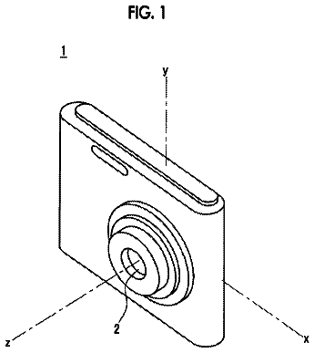
1 of 8 drawing sheets so far from the published document, cropped to the drawing. Every sheet is in the USPTO PDF.
What the patent claimed, word for word. All of it is now free to use.
Field of the Invention
The present invention relates to a solid-state imaging device and an imaging system.
Description of Related Art
In recent years, imaging systems, such as a video camera and an electronic still camera, have become widespread. In these imaging systems, a charge coupled device (CCD) solid-state imaging device or a complementary metal oxide semiconductor (CMOS) solid-state imaging device is mounted. In these solid-state imaging devices, a plurality of pixels are arranged in a two-dimensional matrix, and a signal charge generated by a photoelectric conversion unit, such as a photodiode, provided in a pixel, on which light is incident, is amplified by an amplification unit provided in the pixel and is output as a pixel signal. At this time, in a general CMOS solid-state imaging device, hitherto, the pixel signals from the pixels arranged in a two-dimensional matrix have been sequentially read for each row.
A CMOS solid-state imaging device can be manufactured using a general semiconductor manufacturing process while a CCD solid-state imaging device is manufactured by a dedicated manufacturing process. From this, the CMOS solid-state imaging device easily realizes multifunctionality by various functional circuits being incorporated into a solid-state imaging device, like a system on chip (SOC). For this reason, in a CMOS solid-state imaging device (hereinafter, referred to as a “solid-state imaging device”) mounted in an imaging system, there are an increasing number of examples where a solid-state imaging device has an internal analog-to-digital conversion circuit and pixel data obtained by performing analog-to-digital conversion on the pixel signals read from the pixels is output.
With recent increases in the speed of solid-state imaging devices, a transfer rate of pixel data between a solid-state imaging device in an imaging system and an image processing unit has been improved. In solid-state imaging devices, it is known that an improvement of a data transfer rate is coped with by improving a clock frequency when transferring pixel data to be output corresponding to a low voltage differential signaling system (LVDS), which is a differential interface system, or by increasing the bus width of a data bus for transferring pixel data to an image processing unit.
However, if the clock frequency in transferring pixel data from the solid-state imaging device to the image processing unit increases or the bus width of the data bus increases, the power consumption of the solid-state imaging device also increases. For this reason, a conventional general solid-state imaging device is provided with a mechanism for changing the number of bits of pixel data of one pixel (see Japanese Unexamined Patent Application, First Publication No. 2009-182412).
In an imaging system in which a solid-state imaging device provided with a mechanism for changing the number of bits of pixel data is mounted, the number of bits of pixel data transferred from the solid-state imaging device to the image processing unit is changed according to the operation mode of the imaging system. For example, in a case where the operation mode of the imaging system is a still image mode for capturing a still image, 12-bit pixel data is transferred from the solid-state imaging device to the image processing unit, and in a case of the operation mode for capturing a moving image, 10-bit pixel data is transmitted from the solid-state imaging device to the image processing unit. Furthermore, for example, in a case where the operation mode of the imaging system is a live view mode for displaying a confirmation image (a live view image (through image)) for confirming an object to be imaged on a display device, 9-bit pixel data is transferred, whereby the number of bits of pixel data transferred from the solid-state imaging device to the image processing unit is further reduced.
In this way, in an imaging system in which a solid-state imaging device provided with a mechanism for changing the number of bits of pixel data is mounted, the number of bits of pixel data transferred from the solid-state imaging device to the image processing unit is changed according to the operation mode, thereby reducing the power consumption of the solid-state imaging device and the imaging system.
A solid-state imaging device in accordance with an embodiment of the present invention includes: a pixel signal processing unit which has a plurality of pixels disposed in a two-dimensional matrix, outputs each of pixel signals generated by all of the plurality of pixels disposed as a total pixel signal, and outputs each of the pixel signals generated by the plurality of pixels with the number of pixels reduced to a prescribed number of pixels as a reduced pixel signal; a bit reduction method determination unit which determines a bit reduction method for reducing the number of bits of a digital value representing an amount of the total pixel signal based on the reduced pixel signal; and a bit reduction unit which reduces the number of bits of the digital value based on the bit reduction method determined by the bit reduction method determination unit and outputs the digital value with the reduced number of bits as a digital value corresponding to the total pixel signal.
In the solid-state imaging device, the reduced pixel signal may be a pixel signal obtained by averaging the pixel signals generated by a plurality of corresponding pixels among the plurality of pixels in a same exposure period.
In the solid-state imaging device, the reduced pixel signal may be a pixel signal generated by one prescribed pixel among the pixel signals generated by a plurality of corresponding pixels among the plurality of pixels in the same exposure period.
The solid-state imaging device may further include: a difference calculation unit which outputs a digital value of a difference between the digital value representing the amount of the total pixel signal and a digital value representing an amount of the reduced pixel signal. The bit reduction unit may reduce the number of bits of the digital value of the difference based on the bit reduction method and outputs the digital value of the difference with the reduced number of bits as the digital value corresponding to the total pixel signal.
In the solid-state imaging device, the bit reduction method determination unit may examine an entire dynamic range of the total pixel signal based on the reduced pixel signal and determine the number of bits allocated to the digital value corresponding to the total pixel signal according to a level of the examined dynamic range.
In the solid-state imaging device, the bit reduction method determination unit may examine an entire brightness distribution of the total pixel signal based on the reduced pixel signal and determine the range of bits allocated to the digital value corresponding to the total pixel signal based on the examined brightness distribution.
In the solid-state imaging device, the bit reduction method determination unit may examine an entire contrast value of the total pixel signal based on the reduced pixel signal and determine the number of bits allocated to the digital value corresponding to the total pixel signal according to a level of the examined contrast value.
An imaging system in accordance with an embodiment of the present invention includes the solid-state imaging device. The bit reduction method determination unit may determine the bit reduction method based on information representing conditions for performing imaging with the solid-state imaging device in addition to the reduced pixel signal.
In the imaging system, the information representing the conditions for performing imaging may be control information of a lens including at least one of aperture information and focusing information of the lens which forms an optical image of an object on the solid-state imaging device.
FIG. 1 is a block diagram showing the schematic configuration of an imaging system in which a solid-state imaging device is mounted in an embodiment of the invention.
FIG. 2 is a block diagram showing the schematic configuration of a solid-state imaging device in a first embodiment of the invention.
FIG. 3 is a diagram showing a read sequence of pixel signals in the solid-state imaging device of the first embodiment.
FIGS. 4A and 4B are diagrams illustrating a first bit reduction method in the solid-state imaging device of the first embodiment.
FIGS. 5A to 5C are diagrams illustrating a second bit reduction method in the solid-state imaging device of the first embodiment.
FIG. 6 is a block diagram showing the schematic configuration of a solid-state imaging device in a second embodiment of the invention.
FIG. 7 is a block diagram showing the schematic configuration of a solid-state imaging device in a third embodiment of the invention.
FIGS. 8A to 8D are diagrams illustrating a bit reduction method in the solid-state imaging device of the third embodiment.
Hereinafter, an embodiment of the invention will be described referring to the drawings. FIG. 1 is a block diagram showing the schematic configuration of an imaging system in which a solid-state imaging device is mounted in this embodiment. In FIG. 1 , an imaging system 1 includes a solid-state imaging device 10 , an image processing unit 20 , a display device 30 , a dynamic random access memory (DRAM) 40 , and a recording medium 50 . The image processing unit 20 includes an imaging processing unit 210 , an evaluation value generation unit 211 , a still image processing unit 221 , a moving image processing unit 222 , a display processing unit 230 , a DRAM controller 240 , an image recognition unit 250 , a CPU 260 , and a card interface unit 270 .
The solid-state imaging device 10 is the solid-state imaging device of this embodiment which photoelectrically converts an optical image of an object formed by a lens (not shown). The solid-state imaging device 10 outputs pixel data based on pixel signals according to object light to the imaging processing unit 210 in the image processing unit 20 . The solid-state imaging device 10 will be described below.
The image processing unit 20 generates an image subjected to various kinds of prescribed image processing based on pixel data input from the solid-state imaging device 10 and transfers (writes) data (hereinafter, referred to as “image data”) of the generated image to the DRAM 40 . The image processing unit 20 reads image data stored in the DRAM 40 and subjects image data to various kinds of prescribed image processing.
The imaging processing unit 210 , the evaluation value generation unit 211 , the still image processing unit 221 , the moving image processing unit 222 , the display processing unit 230 , the DRAM controller 240 , the image recognition unit 250 , the CPU 260 , and the card interface unit 270 in the imaging system 1 are connected to one another through a data bus 290 . For example, reading of data from the DRAM 40 connected to the DRAM controller 240 and writing of data to the DRAM 40 are performed by direct memory access (DMA).
The imaging processing unit 210 subjects pixel data input from the solid-state imaging device 10 to pre-processing, such as shading correction or pixel defect correction and transfers (writes) image data (hereinafter, referred to as “pre-processed image data”) as a result of the pre-processing to the DRAM 40 .
The evaluation value generation unit 211 provided in the imaging processing unit 210 generates an evaluation value for controlling auto exposure (AE), auto focus (AF), or auto white balance (AWB) based on pre-processed image data as a result of the pre-processing and transfers (writes) the generated evaluation value to the DRAM 40 .
The still image processing unit 221 acquires (reads) pre-processed image data stored in the DRAM 40 and performs various kinds of image processing for recording a still image including demosaic processing (denoising, YC conversion processing, resize processing) and JPEG compression processing to generate still image data. The still image processing unit 221 acquires (reads) still image data recorded in the DRAM 40 and performs various kinds of image processing for reproducing a still image including JPEG decompression processing to generate still image data for display. The still image processing unit 221 transfers (writes) the generated still image data and still image data for display to the DRAM 40 .
The moving image processing unit 222 acquires (reads) pre-processed image data recorded in the DRAM 40 and performs various kinds of image processing for recording a moving image including demosaic processing (denoising, YC conversion processing, resize processing) and moving image compression processing, such as MPEG compression processing or H.264 compression processing, to generate moving image data. The moving image processing unit 222 may generate moving image data for display for reproducing a moving image without subjecting image data subjected to demosaic processing to moving image compression processing. The moving image processing unit 222 acquires (reads) moving image data recorded in the DRAM 40 and performs various kinds of image processing for reproducing a moving image including moving image decompression processing, such as MPEG decompression processing or H.264 decompression processing, to generate moving image data for display. The moving image processing unit 222 transfers (writes) the generated moving image data and moving image data for display to the DRAM 40 .
The display processing unit 230 acquires (reads) image data for display recorded in the DRAM 40 and subjects the acquired image data for display to display processing, such as processing for superimposing data for on-screen display (OSD). The display processing unit 230 outputs and displays image data after the display processing to and on the display device 30 .
The display device 30 is a display device, such as a thin-film transistor (TFT) liquid crystal display (LCD) or an electronic view finder (EVF), and displays an image according to image data after the display processing output from the display processing unit 230 . The display device 30 may be an external display, such as an organic electro luminescence (EL) display, or a television.
The image recognition unit 250 acquires (reads) pre-processed image data recorded in the DRAM 40 , detects a motion amount or a face of an object included in a captured image based on the acquired pre-processed image data, generates information of the detected object, and transfers (writes) the generated information to the DRAM 40 . The image recognition unit 250 recognizes a scene of the captured image based on the acquired pre-processed image data, generates information of the recognized scene, and transfers (writes) the generated information to the DRAM 40 . The image recognition unit 250 may hold the generated information of the object or information of the scene in a register in the image recognition unit 250 without transferring information to the DRAM 40 .
The card interface unit 270 acquires (reads) still image data or moving image data recorded in the DRAM 40 and records the acquired image data in the recording medium 50 . The card interface unit 270 reads still image data or moving image data recorded in the recording medium 50 and transfers (writes) the read image data to the DRAM 40 .
The recording medium 50 is a recording medium, such as an SD memory card, and records still image data or moving image data output from the card interface unit 270 . Still image data or moving image data recorded by the card interface unit 270 is read. In FIG. 1 , although the recording medium 50 is included as a component of the imaging system 1 , the recording medium 50 is detachably mounted in the imaging system 1 .
The DRAM controller 240 performs the transfer (write) of data to the DRAM 40 connected thereto and the acquisition (read) of data from the DRAM 40 according to an access request to the DRAM 40 from a plurality of components in the imaging system 1 connected to the data bus 290 , for example, a DMA access request.
The DRAM 40 is a memory in which access control is performed by the DRAM controller 240 . The DRAM 40 temporarily stores various kinds of data during processing of the components in the imaging system 1 .
The CPU 260 controls the components of the imaging system 1 , that is, the entire imaging system 1 . For example, the CPU 260 controls the operations of the components in the imaging system 1 according to an imaging operation or a reproduction operation in the imaging system 1 . Furthermore, for example, the CPU 260 controls a lens (not shown) when the imaging system 1 performs the imaging operation. First Embodiment
Next, the solid-state imaging device 10 mounted in the imaging system 1 of this embodiment will be described. FIG. 2 is a block diagram showing the schematic configuration of a solid-state imaging device 10 in a first embodiment. The solid-state imaging device 10 shown in FIG. 2 has a pixel signal processing unit 100 , a first reading unit 110 , a second reading unit 120 , and a transfer unit 130 .
The pixel signal processing unit 100 includes a pixel array in which a plurality of pixels are formed to be arranged in a two-dimensional matrix. The pixel signal processing unit 100 outputs pixel signals obtained by photoelectrically converting light incident on the pixels to the corresponding one of the first reading unit 110 or the second reading unit 120 according to a reading control signal input from each of the first reading unit 110 and the second reading unit 120 . The pixel signal processing unit 100 can separately output each of the pixel signals of all pixels disposed in the pixel array as a total pixel signal S 1 and each of the pixel signals of pixels with the number of pixels disposed in the pixel array reduced as a reduced pixel signal S 2 . The pixel signal processing unit 100 outputs each total pixel signal S 1 to the first reading unit 110 according to the reading control signal input from the first reading unit 110 . The pixel signal processing unit 100 outputs each reduced pixel signal S 2 to the second reading unit 120 according to the reading control signal input from the second reading unit 120 .
The first reading unit 110 reads each total pixel signal S 1 from the pixel signal processing unit 100 and outputs a digital value obtained by performing analog-to-digital conversion on each read total pixel signal S 1 to the transfer unit 130 . At this time, the first reading unit 110 reduces the number of bits of each total pixel signal S 1 subjected to analog-to-digital conversion and output according to a bit reduction control signal input from the second reading unit 120 and outputs each total pixel signal S 1 to the transfer unit 130 .
The second reading unit 120 reads each reduced pixel signal S 2 from the pixel signal processing unit 100 and determines a method of reducing the number of bits of the digital value of each total pixel signal S 1 subjected to analog-to-digital conversion and output from the first reading unit 110 based on each read reduced pixel signal S 2 . The second reading unit 120 outputs a bit reduction control signal representing the determined bit reduction method to the first reading unit 110 .
The transfer unit 130 transfers the digital value of each total pixel signal S 1 with the reduced number of bits output from the first reading unit 110 to the outside as pixel data. That is, the transfer unit 130 transfers (outputs) pixel data with the reduced number of bits to the imaging processing unit 210 in the image processing unit 20 .
With this configuration, the solid-state imaging device 10 reduces the number of bits of each piece of pixel data of based on the pixel signals of all pixels provided in the pixel signal processing unit 100 and outputs pixel data to the imaging processing unit 210 in the image processing unit 20 .
Next, the components of the solid-state imaging device 10 of the first embodiment will be described in more detail. First, the configuration of the pixel signal processing unit 100 of the solid-state imaging device 10 of the first embodiment shown in FIG. 2 will be described in more detail. In the solid-state imaging device 10 , as described above, although the pixel array having a plurality of pixels disposed in a two-dimensional matrix is provided in the pixel signal processing unit 100 , for ease of description. FIG. 2 shows an example of a case where four pixels including a pixel a to a pixel d are disposed in the pixel signal processing unit 100 provided in the solid-state imaging device 10 . Although the solid-state imaging device 10 is provided with components, such as a vertical scanning circuit and a horizontal scanning circuit, which drive the components of the pixels disposed in the pixel signal processing unit 100 under the control of a control device (for example, the CPU 260 or the like in the image processing unit 20 ), which is provided in the imaging system 1 with the solid-state imaging device 10 mounted therein and controls the solid-state imaging device 10 , these components are not shown in FIG. 2 .
In the following description, in order to distinguish the pixels corresponding to the components, that is, the pixel a to the pixel d, the mark “a”, “b”, “c”, or “d” indicating the corresponding pixel is attached to the end of the reference numeral of each component. Specifically, “a” is attached to the end of the reference numeral of each component corresponding to the pixel a. “b” is attached to the end of the reference numeral of each component corresponding to the pixel b, “c” is attached to the end of the reference numeral of each component corresponding to the pixel c, and “d” is attached to the end of the reference numeral of each component corresponding to the pixel d. The marks “a” to “d” are not attached to the components commonly corresponding to the pixel a to the pixel d. In a case where a component corresponds to one of the pixel a to the pixel d, but the corresponding pixel is not distinguished for description, the marks “a” to “d” are not shown, and only the reference numerals of the components are shown.
The pixel signal processing unit 100 of the solid-state imaging device 10 of the first embodiment shown in FIG. 2 has four photoelectric conversion units 101 a to 101 d , four charge transfer circuits 102 a to 102 d , four first charge storage circuits 103 a to 103 d , and two second charge storage circuits 104 ab and 104 cd . In the pixel signal processing unit 100 of the solid-state imaging device 10 of the first embodiment shown in FIG. 2 , the components including the photoelectric conversion unit 101 a , the charge transfer circuit 102 a , and the first charge storage circuit 103 a constitute the pixel a, and the components including the photoelectric conversion unit 101 b , the charge transfer circuit 102 b , and the first charge storage circuit 103 b constitute the pixel b. Furthermore, the components including the photoelectric conversion unit 101 c , the charge transfer circuit 102 c , and the first charge storage circuit 103 c constitute the pixel c, and the components including the photoelectric conversion unit 101 d , the charge transfer circuit 102 d , and the first charge storage circuit 103 d constitute the pixel d. The second charge storage circuit 104 ab is a common component for the pixel a and the pixel b, and the second charge storage circuit 104 cd is a common component for the pixel c and the pixel d.
Each of the photoelectric conversion unit 101 a to the photoelectric conversion unit 101 d is a photoelectric conversion unit, such as a photodiode, which photoelectrically converts incident light to generate a signal charge and stores the generated signal charge.
Each of the charge transfer circuit 102 a to the charge transfer circuit 102 d is a circuit which transfers the signal charge generated and stored in the corresponding one of the photoelectric conversion unit 101 a to the photoelectric conversion unit 101 d to the corresponding one of the first charge storage circuit 103 a to the first charge storage circuit 103 d and the corresponding one of the second charge storage circuit 104 ab and the second charge storage circuit 104 cd.
Each of the first charge storage circuit 103 a to the first charge storage circuit 103 d is a circuit which holds (stores) the signal charge transferred from the corresponding one of the charge transfer circuit 102 a to the charge transfer circuit 102 d and generated in the corresponding one of the photoelectric conversion unit 101 a to the photoelectric conversion unit 101 d . Furthermore, each of the first charge storage circuit 103 a to the first charge storage circuit 103 d is a circuit which outputs, according to the reading control signal input from a first reading control unit 1101 in the corresponding first reading unit 110 , a signal voltage according to the held signal charge as each pixel signal of the total pixel signals S 1 to a first A/D conversion unit 1102 in the first reading unit 110 .
Each of the second charge storage circuit 104 ab and the second charge storage circuit 104 cd is a circuit (averaged charge storage circuit) which holds (stores) a signal charge of a charge amount obtained by averaging the charge amount of the signal charge transferred from the corresponding one of the charge transfer circuit 102 a to the charge transfer circuit 102 d and generated in the corresponding one of the photoelectric conversion unit 101 a to the photoelectric conversion unit 101 d , or a signal charge for averaging the charge amount of the signal charge. That is, each of the second charge storage circuit 104 ab and the second charge storage circuit 104 cd is a circuit which adds and averages the signal charges of the pixels provided in the pixel signal processing unit 100 of the solid-state imaging device 10 and holds a signal charge for placing a state in which the number of pixels provided in the pixel signal processing unit 100 is reduced. Furthermore, each of the second charge storage circuit 104 ab and the second charge storage circuit 104 cd is a circuit which outputs, according to the reading control signal input from a second reading control unit 1201 in the corresponding second reading unit 120 , a signal voltage according to the held signal charge as each reduced pixel signal S 2 in a state of the reduced number of pixels to a second A/D conversion unit 1202 in the second reading unit 120 .
In the pixel signal processing unit 100 of the solid-state imaging device 10 of the first embodiment shown in FIG. 2 , the second charge storage circuit 104 ab corresponds to the charge transfer circuit 102 a and the charge transfer circuit 102 b , that is, the photoelectric conversion unit 101 a and the photoelectric conversion unit 101 b . Furthermore, the second charge storage circuit 104 cd corresponds to the charge transfer circuit 102 c and the charge transfer circuit 102 d , that is, the photoelectric conversion unit 101 c and the photoelectric conversion unit 101 d.
A configuration which adds and averages the signal charges of the pixels to reduce the number of pixels may be, for example, a configuration in which the signal charges generated in the photoelectric conversion unit 101 a and the photoelectric conversion unit 101 b are added and averaged for holding the signal charges in the second charge storage circuit 104 ab , a configuration in which the signal charges held in the second charge storage circuit 104 ab are added and averaged for outputting a signal voltage of each signal charge, or the like. For example, a configuration in which the signal charges held in the second charge storage circuit 104 ab are added and averaged after outputting a signal voltage according to each signal charge may be made.
With such a configuration, the pixel signal processing unit 100 exposes the pixels in the same exposure period, holds the signal charges generated in the pixels by the photoelectric conversion units 101 in the first charge storage circuits 103 , and holds the signal charges (the signal charges with the reduced number of pixels) obtained by averaging the signal charges in the second charge storage circuits 104 . Specifically, the pixel signal processing unit 100 holds the signal charge generated by the photoelectric conversion unit 101 a in the first charge storage circuit 103 a . The pixel signal processing unit 100 holds the signal charge generated by the photoelectric conversion unit 101 b in the first charge storage circuit 103 b . The pixel signal processing unit 100 holds the signal charge generated by the photoelectric conversion unit 101 c in the first charge storage circuit 103 c . The pixel signal processing unit 100 holds the signal charge generated by the photoelectric conversion unit 101 d in the first charge storage circuit 103 d . The pixel signal processing unit 100 holds the signal charge obtained by averaging the signal charge generated by the photoelectric conversion unit 101 a and the signal charge generated by the photoelectric conversion unit 101 b in the second charge storage circuit 104 ab . The pixel signal processing unit 100 holds the signal charge obtained by averaging the signal charge generated by the photoelectric conversion unit 101 c and the signal charge generated by the photoelectric conversion unit 101 d in the second charge storage circuit 104 cd . The pixel signal processing unit 100 separately outputs the pixel signals according to the signal charges in the first charge storage circuits 103 and the pixel signals according to the signal charges held in the second charge storage circuits 104 . That is, the pixel signal processing unit 100 separately outputs each of the pixel signals (total pixel signal S 1 ) of all pixels provided in the pixel signal processing unit 100 and each of the pixel signals (reduced pixel signal S 2 ) with the number of pixels provided in the pixel signal processing unit 100 reduced based on the signal charges obtained by the same single exposure.
In the solid-state imaging device 10 of the first embodiment shown in FIG. 2 , the configuration of the pixel signal processing unit 100 which includes the second charge storage circuits 104 configured to hold the signal charges obtained by averaging the charge amounts of the signal charges generated by the photoelectric conversion units 101 provided in the pixels with two prescribed pixels as a set has been described. However, in an actual solid-state imaging device, for example, color filters of a Bayer array are attached to the pixel array having a plurality of pixels disposed in a two-dimensional matrix, and the photoelectric conversion units 101 provided in the pixels photoelectrically convert the colors corresponding to the attached color filters included in incident light to generate the signal charges. Accordingly, in the solid-state imaging device 10 of the first embodiment, it is preferable that the sets of pixels are constituted such that the centers of gravity of the colors of the attached color filters are not deviated and the signal charges of different colors are not averaged.
In the pixel signal processing unit 100 of the solid-state imaging device 10 of the first embodiment shown in FIG. 2 , a configuration in which the second charge storage circuit 104 ab and the second charge storage circuit 104 cd add and average the signal charges generated by the photoelectric conversion unit 101 a to the photoelectric conversion unit 101 d to reduce the number of pixels has been described. However, a method of reducing the number of pixels is not limited only to addition-averaging shown in FIG. 2 , and for example, a configuration in which the pixels are thinned to reduce the number of pixels may be made. In this case, in the pixel signal processing unit 100 of the solid-state imaging device 10 of the first embodiment shown in FIG. 2 , a configuration in which the second charge storage circuit 104 ab and the second charge storage circuit 104 cd hold (store) one of the signal charges generated by the photoelectric conversion unit 101 a to the photoelectric conversion unit 101 d to thin the pixels is considered.
Next, the configuration of the first reading unit 110 of the solid-state imaging device 10 of the first embodiment shown in FIG. 2 will be described in more detail. The first reading unit 110 of the solid-state imaging device 10 of the first embodiment shown in FIG. 2 has a first reading control unit 1101 , a first A/D conversion unit 1102 , and a bit reduction unit 1103 .
The first reading control unit 1101 sequentially outputs the reading control signal for sequentially reading the total pixel signals S 1 from the first charge storage circuit 103 a to the first charge storage circuit 103 d in the pixel signal processing unit 100 to the first charge storage circuit 103 a to the first charge storage circuit 103 d.
The first A/D conversion unit 1102 is an A/D conversion circuit which performs analog-to-digital conversion on each total pixel signal S 1 (analog signal) read by the first reading control unit 1101 and sequentially input from each of the first charge storage circuit 103 a to the first charge storage circuit 103 d and sequentially outputs a value (digital value) representing the amount of each total pixel signal S 1 (analog signal) to the bit reduction unit 1103 .
The bit reduction unit 1103 reduces the number of bits of the digital value of each total pixel signal S 1 sequentially input from the first A/D conversion unit 1102 according to the bit reduction control signal input from the bit reduction method determination unit 1205 in the second reading unit 120 by a prescribed method and outputs the digital value of each total pixel signal S 1 with the reduced number of pixels to the transfer unit 130 . A method in which the bit reduction unit 1103 reduces the number of bits of the digital value according to the bit reduction control signal will be described below.
With such a configuration, the first reading unit 110 reads each total pixel signal S 1 held in the first charge storage circuit 103 in the pixel signal processing unit 100 and outputs the digital value obtained by performing analog-to-digital conversion on each read total pixel signal S 1 to the transfer unit 130 . At this time, the first reading unit 110 reduces the number of bits of the digital value of each total pixel signal S 1 subjected to analog-to-digital conversion and output according to the bit reduction control signal input from the second reading unit 120 and outputs the digital value to the transfer unit 130 . With this, the transfer unit 130 outputs the digital value of the total pixel signal S 1 with the reduced number of bits subjected to analog-to-digital conversion input from the first reading unit 110 as pixel data with the reduced number of bits to the outside.
Next, the configuration of the second reading unit 120 of the solid-state imaging device 10 of the first embodiment shown in FIG. 2 will be described in more detail. The second reading unit 120 of the solid-state imaging device 10 of the first embodiment shown in FIG. 2 has a second reading control unit 1201 , a second A/D conversion unit 1202 , and a bit reduction method determination unit 1205 .
The second reading control unit 1201 sequentially outputs the reading control signal for sequentially reading each reduced pixel signal S 2 from the second charge storage circuit 104 ab and the second charge storage circuit 104 cd in the pixel signal processing unit 100 to the second charge storage circuit 104 ab and the second charge storage circuit 104 cd.
The second A/D conversion unit 1202 is an A/D conversion circuit which performs analog-to-digital conversion on each reduced pixel signal S 2 (analog signal) read by the second reading control unit 1201 and sequentially input from each of the second charge storage circuit 104 ab and the second charge storage circuit 104 cd and sequentially outputs a value (digital value) representing the amount of each reduced pixel signal S 2 (analog signal) to the bit reduction method determination unit 1205 .
In a case of a configuration in which each of the second charge storage circuit 104 ab and the second charge storage circuit 104 cd in the pixel signal processing unit 100 outputs the signal voltage according to each held signal charge as it is without performing addition-averaging, a configuration in which the second A/D conversion unit 1202 sequentially outputs the digital value having the amount obtained by adding and averaging the signal voltage output from each of the second charge storage circuit 104 ab and the second charge storage circuit 104 cd to the bit reduction method determination unit 1205 may be made. In this case, the second A/D conversion unit 1202 may add and average each signal voltage sequentially output from each of the second charge storage circuit 104 ab and the second charge storage circuit 104 cd by the second reading control unit 1201 in a state of an analog signal and may then perform analog-to-digital conversion on each signal voltage, or may perform analog-to-digital conversion on each signal voltage and may then add and average each signal voltage in a state of a digital value.
The bit reduction method determination unit 1205 determines the bit reduction method, in which the bit reduction unit 1103 in the first reading unit 110 reduces the number of bits of the digital value of each total pixel signal S 1 , based on the digital value of each reduced pixel signal S 2 sequentially input from the second A/D conversion unit 1202 and outputs the bit reduction control signal representing the determined bit reduction method to the bit reduction unit 1103 in the first reading unit 110 .
With such a configuration, the second reading unit 120 reads each reduced pixel signal S 2 held in each second charge storage circuit 104 in the pixel signal processing unit 100 and determines the bit reduction method to the digital value of each total pixel signal S 1 in the first reading unit 110 based on each digital value obtained by performing analog-to-digital conversion on each read reduced pixel signal S 2 . The second reading unit 120 outputs the bit reduction control signal representing the determined bit reduction method to the first reading unit 110 .
Accordingly, in the solid-state imaging device 10 of the first embodiment, the second reading unit 120 reads each reduced pixel signal S 2 ahead and determines a bit reduction method to the digital value of each total pixel signal S 1 , and then, the first reading unit 110 reduces the number of bits of each digital value obtained by performing analog-to-digital conversion on each total pixel signal S 1 according to the bit reduction control signal and outputs each digital value to the transfer unit 130 .
In the solid-state imaging device 10 of the first embodiment, the timing for reading the total pixel signal S 1 and the reduced pixel signal S 2 from the first charge storage circuit 103 and the second charge storage circuit 104 in the pixel signal processing unit 100 will be described. FIG. 3 is a diagram showing a read sequence of the pixel signals (the total pixel signal S 1 and the reduced pixel signal S 2 ) in the solid-state imaging device 10 of the first embodiment.
The description continues in the full USPTO document.
About 6,713 words. The USPTO PDF has it with every drawing.
Fees are due 3.5, 7.5 and 11.5 years after grant. This patent expired on January 30, 2026, so the fee marked "not paid" was the one that went unpaid.
SOLID-STATE IMAGING DEVICE AND IMAGING SYSTEM
Filed Aug 2016 · published Dec 2016Solid-state imaging device and imaging system using a bit reduction method based on a reduced pixel signal
Filed Aug 2016 · granted Jan 2018Earlier publications, parents and continuations. None of them can still be enforced, or this patent would not be listed.
Prior art cited by the examiner or applicant. Useful when you check your own idea for novelty.
Everything on this page comes from the documents linked above.