 Lapsed, fee not paid6 drawings
Chips & Semiconductors · US 9,871,184 B2
System and a method for emitting an ultrasonic signal
A system for emitting an ultrasonic signal is provided.
US 9,871,225 B2 · Assignee: KONICA MINOLTA, INC. · Inventors: Kuroki; Takaaki et al.
Sheet 1 of 5 from the published document. All sheets in the USPTO PDF
Provided is an organic electroluminescent element including a film substrate having thereon: at least one gas barrier layer, a light scatter layer, at least one smooth layer, and a light-emitting unit containing an organic functional layer interposed between a pair of electrodes, laminated in this order, wherein the light scatter layer contains a binder and light scatter particles having an average particle size of 0.2 μm or more to less than 1 μm; and the smooth layer contains an oxide or a nitride of silicone or niobium as a main component.
In recent years, in the field of electronic devices, there have been added requirements of long-term reliability, flexible shape, and enabling curved display in addition to light weight and large size. The used of a film substrate such as a transparent plastic has been started in place of a glass substrate having a heavy weight and difficult in making a large size. However, a film substrate such as a transparent plastic has a problem of inferior gas barrier property compared with a glass substrate. It has been known that the function of the electronic device will be deteriorated by the penetrated water vapor and oxygen gas when a substrate of inferior gas barrier property is used. It has been generally known to use a gas barrier film produced by forming a film having a gas barrier property (a gas barrier layer) on a film substrate. For example, as a gas barrier film used for package mate
1 of 5 drawing sheets so far from the published document, cropped to the drawing. Every sheet is in the USPTO PDF.
What the patent claimed, word for word. All of it is now free to use.
This is the U.S. national stage of application No. PCT/JP2014/081725, filed on Dec. 1, 2014. Priority under 35 U.S.C. § 119(a) and 35 U.S.C. § 365(b) is claimed from Japanese Application No. 2013-252693, filed Dec. 6, 2013, the disclosure of which is also incorporated herein by reference.
The present invention relates to an organic electroluminescent element achieving a high-temperature storage stability and improved light-emission efficiency while maintaining flexible aptitude.
In recent years, in the field of electronic devices, there have been added requirements of long-term reliability, flexible shape, and enabling curved display in addition to light weight and large size. The used of a film substrate such as a transparent plastic has been started in place of a glass substrate having a heavy weight and difficult in making a large size.
However, a film substrate such as a transparent plastic has a problem of inferior gas barrier property compared with a glass substrate.
It has been known that the function of the electronic device will be deteriorated by the penetrated water vapor and oxygen gas when a substrate of inferior gas barrier property is used.
It has been generally known to use a gas barrier film produced by forming a film having a gas barrier property (a gas barrier layer) on a film substrate. For example, as a gas barrier film used for package material for an object required to be provided with or for a liquid crystal display element, there are a film composed of a film substrate on which silicon oxide or a aluminum oxide is vapor deposited.
It has been reported that a light extraction structure containing a light scatter layer is efficient for the purpose of improving light-emission efficiency of an organic EL (electroluminescence) element (one of electronic devices) (refer to Patent document 1, for example).
When a gas barrier layer or a light scatter layer is formed on a film substrate, it will be produced unevenness on the surface. As a result, when a light-emitting unit having organic functional layers is formed thereon, it may be occurred deterioration of keeping property or short-circuit (electric short) under the environment of high-temperature and high-humidity.
In the first place, it is known that an organic EL element is very sensitive to a small amount of water, oxygen and other organic compounds (such as a remaining solvent). It was proposed a structure having a gas barrier layer directly under an organic functional layer (refer to Patent document 2, for example). It may be a reasonable idea.
However, it has not been disclosed technology to achieve both gas barrier property and bend (curvature) repeating resistance, namely, flexible aptitude. This has not been realized until now. PRIOR ART DOCUMENTS Patent Documents
Patent document 1: JP-A No. 2004-296437
Patent document 2: Japan Patent No. 4186688 SUMMARY OF THE INVENTION Problems to be Solved by the Invention
The present invention has been made in view of the above-described problem and situation. An object of the present invention is to provide an organic electroluminescent element achieving a high-temperature storage stability and improved light-emission efficiency while maintaining flexible aptitude. Means to Solve the Problems
The present inventors have investigated the reasons of the above-described problems to solve the problems, and found out to provide an organic electroluminescent element achieving a high-temperature storage stability and improved light-emission efficiency while maintaining flexible aptitude. The organic electroluminescent element contains: a film substrate having thereon at least one gas barrier layer, a light scatter layer, at least one smooth layer, and a light-emitting unit containing an organic functional layer interposed between a pair of electrodes, laminated in this order. Thus, the present invention has been achieved.
Namely, the above-described problems relating to the present invention are solved by the following embodiments.
1. An organic electroluminescent element comprising a film substrate having thereon: at least one gas barrier layer, a light scatter layer, at least one smooth layer, and a light-emitting unit containing an organic functional layer interposed between a pair of electrodes, laminated in this order,
wherein the light scatter layer contains a binder and light scatter particles having an average particle size of 0.2 μm or more to less than 1 μm; and
the smooth layer contains an oxide or a nitride of silicon or niobium as a main component.
2. An organic electroluminescent element comprising a film substrate having thereon: at least one gas barrier layer, a light scatter layer, at least one smooth layer, and a light-emitting unit containing an organic functional layer interposed between a pair of electrodes, laminated in this order,
wherein the light scatter layer contains a binder and light scatter particles having an average particle size of 0.2 μm or more to less than 1 μm; and
the smooth layer has a water vapor permeability of less than 0.1 g/(m.sup.2.Math.24 h).
3. An organic electroluminescent element described in the embodiment 2,
wherein the smooth layer contains an oxide or a nitride of silicon or niobium as a main component.
4. An organic electroluminescent element described in any one of the embodiments 1 to 3,
wherein the smooth layer contains a reaction product of an inorganic silicon compound or an organic silicon compound, or niobium oxide as a main component.
5. An organic electroluminescent element described in any one of the embodiments 1 to 4,
wherein a water vapor permeability of the gas barrier layer (Wg), a water vapor permeability of the light scatter layer (Ws), and a water vapor permeability of the smooth layer (Wf) satisfy the following conditional expression Wg≦Wf<Ws 6. An organic electroluminescent element described in any one of the embodiments 1 to 4,
wherein the smooth layer has a refractive index in the range of 1.7 to 3.0.
7. An organic electroluminescent element described in any one of the embodiments 1 to 6,
wherein the smooth layer contains nanoparticles having a refractive index in the range of 1.7 to 3.0.
8. An organic electroluminescent element described in any one of the embodiments 1 to 7,
wherein the smooth layer has a first smooth layer and a second smooth layer in a sequential order from a side of the light-emitting unit;
the first smooth layer contains an oxide or a nitride of silicon or niobium as a main component; and
the second smooth layer is formed with a wet process.
9. An organic electroluminescent element described in the embodiment 8,
wherein the first smooth layer is formed with a dry process.
10. An organic electroluminescent element described in the embodiments 8 or 9,
wherein the first smooth layer is formed with a wet process.
11. An organic electroluminescent element described in any one of the embodiments 8 to 10,
wherein at least one of the first smooth layer and the second smooth layer contains nanoparticles having a refractive index in the range of 1.7 to 3.0.
12. An organic electroluminescent element described in any one of the embodiments 8 to 11,
wherein the first smooth layer and the second smooth layer both respectively have a refractive index in the range of 1.7 to 3.0.
13. An organic electroluminescent element described in any one of the embodiments 1 to 12,
wherein the light scatter layer is patterned in a sealing region. Effects of the Invention
By the above-described means of the present invention, it can provide an organic electroluminescent element achieving a high-temperature storage stability and improved light-emission efficiency while maintaining flexible aptitude.
A formation mechanism or an action mechanism of the effects of the present invention is not clarified. However, it is supposed as follows.
Since a light-emission efficiency of an organic EL element will be decreased due to confinement or deactivation of the emitted light in the inside of the element, it is an effective embodiment to place a light extracting structure between the substrate and the electrode. However, such light extracting structure utilizes particles enabling to produce Mie scattering or geometrical scattering, or unevenness of 3 dimensions. These structures are required to be placed between the substrate and the electrode. As a method for forming these structures, various types of methods such as a coating process and a nanoimprint method have been proposed. Many effective methods have been proposed for the glass substrate in the past.
On the other hand, when the above-described light extracting structure is intended to form on a flexible substrate (for example, a film substrate), a high-temperature treatment cannot be done during the formation of the above-described structure due to the small heat resistance of the film substrate. That is the most disadvantage of the film substrate. As a result, a small amount of gas is emitted from the material composing these light extracting structures. An organic EL element is very sensitive to water or the gases emitted from various materials. When an organic EL element is exposed to these, degradation of the initial property of the production will be accelerated. As a result, light-emission efficiency and a lifetime of an organic EL element will be lowered.
An organic EL element of the present invention has a highly effective light extracting structure capable of being formed on a film, and it has a smooth layer made of an oxide or a nitride of silicon or niobium on the light extracting structure. By this specific composition, a predetermined gas barrier property can be obtained without hindering the light extracting efficiency and the flexibility. Consequently, it is supposed that the high-temperature storage stability of a light-emitting element formed on a film substrate is increased and light-emission efficiency is also improved.
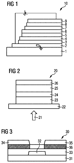
FIG. 1 is a cross-sectional view illustrating a schematic constitution of an organic EL element.
FIG. 2 is a cross-sectional view illustrating a schematic constitution of an organic EL element.
FIG. 3 is a graph indicating of a profile of each element in a layer thickness direction of a gas barrier layer of the present invention with XPS depth element analysis.
FIG. 4 is a schematic drawing illustrating an example of a production apparatus of a gas barrier film.
FIG. 5 is a schematic drawing illustrating positional setting of a deposition gas inlet.
FIG. 6 is a graph indicating of a profile of each element in a layer thickness direction of a gas barrier layer of the present invention with XPS depth element analysis.
FIG. 7 is a graph indicating of a profile of each element in a layer thickness direction of a gas barrier layer for comparison to the present invention with XPS depth element analysis.
An organic electroluminescent element of the present invention contains a film substrate having thereon: at least one gas barrier layer, a light scatter layer, at least one smooth layer, and a light-emitting unit containing an organic functional layer interposed between a pair of electrodes, laminated in this order, wherein the light scatter layer contains a binder and light scatter particles having an average particle size of 0.2 μm or more to less than 1 μm; and the smooth layer contains an oxide or a nitride of silicon or niobium as a main component, or the smooth layer has a water vapor permeability of less than 0.1 g/(m2.Math.24 h). This feature is a common technical feature of the invention according to the embodiments 1 to 13.
In the present invention, in order to effectively prevent penetration of water to result in achieving a prolonged lifetime of an organic EL element, the smooth layer preferably contains a reaction product of an inorganic silicon compound or an organic silicon compound, or niobium oxide as a main component.
In view of storage stability for a long period of time, a water vapor permeability of the gas barrier layer (Wg), a water vapor permeability of the light scatter layer (Ws), and a water vapor permeability of the smooth layer (Wf) satisfy the following conditional expression. Wg≦Wf<Ws
Although it is preferable that the absolute value of Wg is small, the gas permeability of the scatter layer is theoretically large. On the other hand, it is theoretically possible to improve the performance by making Wf to be the lowest among the three. However, the change of the amount of the adsorbed gas of the scatter layer may induce decrease of light-emission efficiency of an element, or degradation of film strength. Therefore, it is preferable to make Wg to be the smallest. In order to make Wg to be small, an effective embodiment is to place a gas barrier layer on the opposite side of the transparent substrate, and to use repeatedly two constituting members composed of a support and a gas barrier layer.
In view of preventing deterioration of light extracting efficiency by the smooth layer, it is preferable that the smooth layer contains nanoparticles having a refractive index in the range of 1.7 to 3.0.
The irregularity of the surface of the formed light scatter layer will be decreased by placing a gas barrier layer. Therefore, it is preferable that: the smooth layer has a first smooth layer and a second smooth layer in a sequential order from a side of the light-emitting unit; the first smooth layer contains an oxide or a nitride of silicon or niobium as a main component; and the second smooth layer is formed with a wet process.
In view of decreasing the amount of water or gasses emitted from various materials penetrating the layers adjacent to the light-emitting element/electrodes, it is preferable that the first smooth layer is formed with a dry process.
Further, in view of improving smoothness of the layers adjacent to the light-emitting element/electrodes, it is preferable that the first smooth layer is formed with a wet process.
In view of preventing deterioration of light extracting efficiency by the smooth layer, it is preferable that the smooth layer has a refractive index in the range of 1.7 to 3.0. For achieving this property, it is preferable that the smooth layer contains nanoparticles having a refractive index in the range of 1.7 to 3.0.
From the viewpoint of improving performance, it is best to achieve the following two: the property of decreasing the amount of water or gasses emitted from various materials penetrating the layers adjacent to the light-emitting element/electrodes; and the property of high smoothness of this layers. From this point, it is preferable that the smooth layer of the present invention is composed of a plurality of layers. These layers may be formed with the same process, or with a different process. These layers may be formed with the same material, or with a different material. As examples of the combination, it can be cited: lamination with a wet process; lamination with a dry process; lamination with a dry process on a layer formed with a wet process; and lamination with a wet process on a layer formed with a dry process. A preferable embodiment is forming a second smooth layer (a layer near to the light scatter layer) with a wet process, and forming a first smooth layer with a dry process.
In the present invention, in order to effectively prevent penetration of water to result in achieving a prolonged lifetime of an organic EL element, the smooth layer preferably contains niobium oxide, or a reaction product of an inorganic silicon compound or an organic silicon compound as a main component. From the viewpoint of light-emission efficiency, the first smooth layer and the second smooth layer both respectively have a refractive index in the range of 1.7 to 3.0. In order to achieve this property, it is particularly preferable that the first smooth layer contains niobium oxide as a main component, and the second smooth layer contains a reaction product of an inorganic silicon compound or an organic silicon compound as a main component.
From the viewpoint of protecting the light scatter layer with a minimum amount of the smooth layer, and preventing penetration of water vapor in the air, it is preferable that the light scatter layer is patterned in a sealing region.
The present invention and the constitution elements thereof, as well as configurations and embodiments, will be detailed in the following. In the present description, when two figures are used to indicate a range of value before and after “to”, these figures are included in the range as a lowest limit value and an upper limit value.
<<Constitution of Organic EL Element>>
An organic EL element of the present invention contains a film substrate having thereon: at least one gas barrier layer, a light scatter layer, at least one smooth layer, and a light-emitting unit containing an organic functional layer interposed between a pair of electrodes, laminated in that order.
Here, “a light-emitting unit” indicates a light-emitting body (unit) mainly composed of organic functional layers such as a light-emitting layer, a hole transport layer, and an electron transport layer. They incorporate various types of organic compounds described later. The light-emitting body is interposed between a pair of electrodes composed of an anode and a cathode. The hole supplied from the anode and the electron supplied from the cathode will be recombined in the light-emitting body to result in producing light.
An organic EL element of the present invention may be provided with a plurality of the light-emitting unit according to the required light-emission color.
Specifically, as illustrated in FIG. 1 , the organic EL element 100 of the present invention is preferably disposed of the following on a film substrate 1 : a gas barrier 2 , a light scatter layer 3 , a smooth layer 4 ( 4 a ), an anode (a transparent electrode) 5 , a light-emitting unit 6 composed of organic materials, and a cathode (an opposite electrode) 7 , which are laminated in that order. This is a preferable embodiment.
An extraction electrode 8 is provided at one end of the transparent electrode 5 (electrode layer 5 b ). The transparent electrode 5 is electrically connected to an external power supply (not illustrated in the figure) through the extraction electrode 8 . The organic EL element 100 is configured such that generated light (emitted light h) is extracted at least from the film substrate 1 .
The organic EL element 100 may have any layer structure, for example, a typical layer structure. Throughout the specification, the transparent electrode 5 functions as an anode and the opposite electrode 7 functions as a cathode. In this case, an exemplary configuration of the light-emitting unit 6 includes: a hole injection layer 6 a /a hole transport layer 6 b /a light-emitting layer 6 c /an electron transport layer 6 d /and an electron injection layer 6 e , sequentially disposed on the transparent electrode 5 as an anode. It is essential existence of the light-emitting layer 6 c composed of at least an organic material among these layers. The hole injection layer 6 a and the hole transport layer 6 b may be disposed of as a hole transport-injecting layer. The electron transport layer 6 d and the electron injection layer 6 e may be disposed of as an electron transport-injecting layer. In the light-emitting unit 6 , the electron injection layer 6 e may be composed of an inorganic material, for example.
The light-emitting unit 6 may include a hole blocking layer and an electron blocking layer disposed in required places if necessary. The light-emitting layer 6 c may include luminous sublayers of different colors generating luminescent lights in the corresponding wavelength regions. These luminous sublayers of different colors and a non-luminous intermediate sublayer may be laminated with the non-luminous intermediate sublayer interposed between the luminous sublayers. The intermediate sublayer may function as a hole blocking layer or an electron blocking layer. The opposite electrode 7 or the cathode may have a laminate structure if necessary. In such a laminate configuration, only the portion of the light-emitting unit 6 interposed between the transparent electrode 5 and the opposite electrode 7 corresponds to the light emission region of the organic EL element 100 .
In the layer configuration as described above, an auxiliary electrode 9 may be disposed on the electrode layer 5 b of the transparent electrode 5 to reduce the resistance of the transparent electrode 5 .
An organic EL element 100 of the present invention may have a smooth layer 4 composed of a smooth layer 4 a (hereafter, it is called as a first smooth layer) and a smooth layer 4 b (hereafter, it is called as a second smooth layer) in this order from the side of the light-emitting unit 6 , as illustrated in FIG. 2 .
The organic EL element 100 having such a configuration is sealed with a sealing material 10 described later, which is disposed over the film substrate 1 to prevent degradation of the organic light-emitting unit 6 composed of an organic material. The sealing material 10 is fixed to the film substrate 1 with an adhesive 11 . The terminals of the transparent electrode 5 (extraction electrode 8 ) and the opposite electrode 7 are kept insulated on the film substrate 1 by the interposed light-emitting unit 6 , and are exposed from the sealing material 10 .
An organic EL element of the present invention may be a so-called tandem structure element in which plural light-emitting units each containing at least one light-emitting layer are laminated.
As an example of a representative element constitution of the tandem structure, it can be cited the following constitution.
Anode/First Light-Emitting Unit/Intermediate Layer/Second Light-Emitting Unit/Intermediate Layer/Third Organic Light-Emitting Unit/Cathode
Here, the above-described first light-emitting unit, second light-emitting unit, and third organic light-emitting unit may be the same or different. It may be possible that two of the light-emitting units are the same, and the remaining one is different.
In addition, plural light-emitting units each may be laminated directly or they may be laminated through an intermediate layer.
The intermediate layer is also called as: an intermediate electrode, an intermediate conductive layer, a charge generating layer, an electron extraction layer, a connecting layer, and an intermediate insulating layer. Known composing materials may be used as long as it can form a layer which has a function of supplying an electron to an adjacent layer to the anode, and a hole to an adjacent layer to the cathode.
Examples of a material used in an intermediate layer are: conductive inorganic compounds such as ITO (indium tin oxide), IZO (indium zinc oxide), ZnO.sub.2, TiN, ZrN, HfN, TiO.sub.X, VO.sub.X, CuI, InN, GaN, CuAlO.sub.2, CuGaO.sub.2, SrCu.sub.2O.sub.2, LaB.sub.6, RuO.sub.2, and Al; a two-layer film such as Au/Bi.sub.2O.sub.3; a multi-layer film such as SnO.sub.2/Ag/SnO.sub.2, ZnO/Ag/ZnO, Bi.sub.2O.sub.3/Au/Bi.sub.2O.sub.3, TiO.sub.2/TiN/TiO.sub.2, and TiO.sub.2/ZrN/TiO.sub.2; fullerene such as C.sub.60; and a conductive organic layer such as oligothiophene, metal phthalocyanine, metal-free phthalocyanine, metal porphyrin, and metal-free porphyrin. The present invention is not limited to them.
A preferable constitution for a light-emitting unit is a structure of the above-described representative element constitution from which the anode and the cathode are removed. However, the present invention is not limited to that.
Examples of a tandem type organic EL element are described in: U.S. Pat. No. 6,337,492, U.S. Pat. No. 7,420,203, U.S. Pat. No. 7,473,923, U.S. Pat. No. 6,872,472, U.S. Pat. No. 6,107,734, U.S. Pat. No. 6,337,492, WO 2005/009087, JP-A 2006-228712, JP-A 2006-24791, JP-A 2006-49393, JP-A 2006-49394, JP-A 2006-49396, JP-A 2011-96679, JP-A 2005-340187, JP Patent 4711424, JP Patent 3496681, JP Patent 3884564, JP Patent 4213169, JP-A 2010-192719, JP-A 2009-076929, JP-A 2008-078414, JP-A 2007-059848, JP-A 2003-272860, JP-A 2003-045676, and WO 2005/094130. The constitutions of the elements and the composing materials are described in these documents, however, the present invention is not limited to them.
Main constituting components and their preparation method of an organic EL element 100 will be described in the following.
<<Smooth Layer (First Smooth Layer)>>
A first smooth layer 4 a according to the present invention is characterized in that: it has oxide or nitride of silicon (Si) or niobium (Nb) as a main component; and it has a water vapor permeability of less than 0.1 g/(m.sup.2.Math.24 h). By these features, it can effectively prevent penetration of gas emitted from a light scater layer 3 and a second smooth layer (described later) and water in the air. At the same time, it can prevent harmful effects of deterioration of keeping property or short-circuit (electric short) under the environment of high-temperature and high-humidity.
Here, “a main component” indicates a component having a maximum constituting ratio among all of the components constituting the first smooth layer 4 a.
A water vapor permeability of the first smooth layer 4 a is a value determined by the method based on JIS K 7129-1992.
A preferred water vapor permeability is 0.1 g/(m.sup.2.Math.24 h) or less, more preferably, it is 0.01 g/(m.sup.2.Math.24 h) or less, and still more preferably, it is 0.001 g/(m.sup.2.Math.24 h) or less.
A refractive index of the first smooth layer 4 a is preferably in the range of 1.7 to 3.0, more preferably, it is in the range of 1.7 to 2.5, and still more preferably, it is in the range of 1.7 to 2.2. A refractive index of the present invention is a value measured at wavelength of 633 nm with an ellipsometer at 25° C.
When the first smooth layer is made of a low refractive material (having a refractive index of less than 1.7), a thinner layer thickness is preferable. Specifically, a preferable layer thickness is less than 100 nm. The first smooth layer of the present invention preferably has a predetermined gas barrier property. By taking this point into consideration, the layer thickness of the continuous film has the lower limit. It is required that the thickness is 5 nm or more, more preferably it is 10 nm or more, and still more preferably it is 30 nm or more.
On the other hand, when the first smooth layer is made of a high refractive material (having a refractive index of 1.7 or more), there is no limitation to the upper limit of the layer thickness. The lower limit is the same as in the case of the above-described layer made of a low refractive material. With the condition that when the first smooth layer absorbs visible light, a thinner layer thickness is preferable. An optimum layer thickness may be determined from the viewpoint of a required gas barrier property and a light extracting efficiency
It is preferable that a 100 nm thick layer has small absorption in the entire visible region (it is a value obtained by spectral wavelength measurement with an integrating sphere after removing the total value of T % and R %). Preferably it is less than 10%, more preferably it is less than 5%, still more preferably it is less than 3%, and most preferably it is less than 1%.
Further, in the present invention, the bending resistance of a film having a thickness of 100 nm is important. A PET film is provided with a gas barrier film thereon, and then, a film having a thickness of 100 nm is formed. This sample is subjected to a bending test of repeating 100 times of bending. A preferable result is to generate a crack having a diameter of 30 mmΦ or less, more preferably a diameter of 15 mmΦ or less, and still more preferably a diameter of 10 mmΦ or less.
In the following, as film forming methods, a case of a dry process and a case of a wet process are described separately.
<Film Formation with a Dry Process>
Examples of an oxide or a nitride of silicon and niobium are: reaction products of an inorganic silicon compound and an organic silicon compound, niobium oxide, niobium oxynitride, niobium nitride, niobium oxycarbide, and niobium carbo-nitride.
Examples of a reaction product of an inorganic silicon compound are: silicon oxide, silicon oxynitride, silicon nitride, silicon oxycarbide, and silicon carbo-nitride.
Examples of an organic silicon compound are: hexamethyldisiloxane, 1,1,3,3-tetramethyldisiloxane, vinyl trimethylsilane, trimethylsilane, hexamethyldisilane, methylsilane, dimethylsilane, trimethylsilane, diethylsilane, propylsilane, phenylsilane, vinyl triethoxysilanesilane, vinyltrimethoxysilane, tetramethoxysilane, tetraethoxysilane, phenyltrimethoxysilane, methyltriethoxysilane, and octamethylcyclotetrasiloxane. Among these organic silicon compounds, hexamethyldisiloxan and 1,1,3,3-tetramethyldisiloxane are preferably used from the viewpoint of handling during layer formation and light distribution property of the obtained second gas barrier layer. Further, these organic silicon compounds may be used singly, or may be used in combination of two or more.
When a first smooth layer 4 a containing a reaction product of hexamethyldisiloxane is formed, the mole quantity (flow rate) of oxygen is preferably not more than 12 times, which is the stoichiometric ratio, more preferably not more than 10 times that of the hexamethyldisiloxane, which is the raw material gas. With such contents of hexamethyldisiloxane and oxygen, the carbon atoms and hydrogen atoms in the hexamethyldisiloxane that are not completely oxidized are incorporated in the first smooth layer 4 a , enabling to form a desired first smooth layer 4 a . In this view, the lower limit of the mole quantity (flow rate) of oxygen relative to the mole quantity (flow rate) of hexamethyldisiloxane in the deposition gas is preferably 0.1 times or more of the mole quantity (flow rate) of hexamethyldisiloxane, more preferably 0.5 times or more.
When a first smooth layer 4 a made of niobium oxide is formed, the following film forming apparatus may be used. The apparatus contains an RF magnetron plasma generating section and a target composed of niobium oxide (Nb.sub.2O.sub.5) to which spattering in made with plasma generated by the RF magnetron plasma generating section. These are connected to a vacuum treating chamber through an introducing section. The film forming apparatus has an RF magnetron spatter source composed of the RF magnetron plasma generating section and the target. An argon gas plasma is produced by the RF magnetron plasma generating section. By applying the voltage to the disk type target, niobium and oxygen atoms are spattered (RF magnetron spattering), and these are adhered to the substrate located in the downstream. Thus film formation can be done.
It may be formed with a method disclosed in JP-A No. 2006-28634. This method uses a niobium metal as a target. At the moment of forming a niobium oxide film on a substrate surface with a spattering method, an introduction amount of reaction gas is adjusted with a plasma emission monitoring (PME) method. By controlling the intensity of plasma generated from the niobium metal, it may be effectively formed a niobium oxide film excellent in film forming rate and realizing an excellent optical property.
Among these, as an oxide or a nitride of silicon and niobium contained in the first smooth layer 4 a , specifically preferred are: silicon nitride, silicon oxynitride, and niobium oxide.
When a dry process is used for forming a film, a stoichiometric composition will be hardly realized due to the presence of a small amount of gas beside the introduced gas. Specifically, the most representative stoichiometric composition is SiO.sub.2. However, in reality, the formed film has SiO.sub.x (x=1.9 to 2.1) with a composition range. In the present invention, these compounds are treated as SiO.sub.2.
The above-described atom number ratio may be determined with a known method. An example thereof is to use an analytical apparatus using an X-ray photoelectron spectroscopy (XPS).
Examples of a dry process are: a vapor deposition method (a resistance heating method, an electron beam vapor deposition (EB) method), a sputtering method and an ion plating method. Any method may be suitably used as long as it can form a film of a low film stress and high density with having small water vapor permeability.
<Film Formation with a Wet Process>
When the first smooth layer 4 a is produced with a wet process, it is preferable that the layer contains a silicon dioxide compound that is a reaction product of an inorganic silicon compound. In particular, polysilazane is preferably used for forming this film. However, the present invention is not limited to that, and any known materials may be used.
It may be used polysilazane represented by Formula (A) that is used for a light scatter layer 3 .
In Formula, R.sup.1, R.sup.2, and R.sup.3 each independently represent a hydrogen atom, an alkyl group, an alkenyl group, a cycloalkyl group, an aryl group, an alkylsilyl group, an alkylamino group, or an alkoxy group.
From the viewpoint of the density of the first smooth layer 4 a , most preferred is a compound having all of R.sup.1, R.sup.2, and R.sup.3 of hydrogen atoms. That is, perhydropolysilazane (PHPS) is particularly preferable.
The first smooth layer 4 a is formed by applying a coating liquid containing polysilazane, then, the coated layer is dried and irradiated with vacuum ultraviolet rays.
As an organic solvent to prepare a polysilazane containing coating liquid, it is preferable to avoid an alcohol solvent or water which easily reacts with polysilazane. Example of an applicable organic solvent are: a hydrocarbon solvent such as an aliphatic hydrocarbon, an alicyclic hydrocarbon, and an aromatic hydrocarbons; an halogenated hydrocarbon solvent; and ether such as an aliphatic ether and an alicyclic ether. Specific examples thereof are: a hydrocarbon such as pentane, hexane, cyclohexane, toluene, xylene, Solvesso™, and turpentine; a halogenated hydrocarbon such as methylene chloride and trichloroethane; and ether such as dibutyl ether, dioxane and tetrahydrofuran. These organic solvents may be chosen in accordance with characteristics, such as solubility of polysilazane, and an evaporation rate of an organic solvent, and a plurality of solvents may be mixed.
A concentration of polysilazane in a polysilazane containing coating liquid is different depending on the thickness of the first smooth layer 4 a and the pot life of the coating liquid. Preferably, it is in the range of about 0.2 to 35 mass %.
In order to promote the conversion to silicon oxynitride, the polysilazane containing coating liquid for forming a second gas barrier layer may contain additives. Examples thereof are: an amine catalyst, and a metal catalyst (Pt compound such as Pt acetyl acetonate, a Pd compound such as propionic acid PD, a Rh compound such as Rh acetyl acetonate). In the present invention, an amine catalyst is particularly preferable. Specific examples of an amine catalyst are: N,N-diethylethanolamine, N,N-dimethylethanolamine, triethanolamine, triethylamine, 3-morpholino-propylamine, N,N,N′,N′-tetramethyl-1,3-diaminopropane, and N,N,N′,N′-tetramethyl-1,6-diaminohexane.
An added amount of these catalyst to polysilazane is preferably in the range of 0.1 to 10 mass % with respect to the total mass of the coating liquid for forming a second gas barrier layer. More preferably, it is in the range of 0.2 to 5 mass %, and still more preferably, in the range of 0.5 to 2 mass %. By making the concentration of a catalyst in this range, it is possible to avoid excessive formation of silanol due to a rapid advance in reaction such as decrease of a layer density and increase of layer defects.
A conventionally known appropriate wet coating method, may be adopted as a coating method of a polysilazane containing coating liquid. Specific examples of a coating method include: a roller coat method, a flow coat method, an inkjet method, a spray coat method, a printing method, a dip coat method, a casting film forming method, a bar coat method and a gravure printing method.
A coating thickness may be appropriately set up according to the purpose. For example, a coating thickness may be set up to be in the range of 20 nm to 2 μm, more preferably, it is in the range of 30 nm to 1.5 μm, still more preferably, it is in the range of 40 nm to 1 μm.
<Excimer Treatment>
The first smooth layer 4 a according to the present invention is subjected to a process in which a polysilazane containing layer is irradiated with vacuum ultraviolet (VUV) rays. At least a part of polysilazane is reformed to silicon oxynitride by this process.
In a vacuum ultraviolet ray irradiation process of the present invention, illuminance of the aforesaid vacuum ultraviolet rays which are received at a coated layer surface of a polysilazane coated layer is preferably in the range of 30 to 200 mW/cm.sup.2, and more preferably, it is in the range of 50 to 160 mW/cm.sup.2. When it is 30 mW/cm.sup.2 or more, the reforming efficiency will not be decreased. When it is 200 mW/cm.sup.2 or less, there will not occur concern of producing ablation in the coated layer or giving damage to the substrate.
An amount of irradiation energy (irradiation amount) of vacuum ultraviolet rays at a polysilazane coated layer surface is preferably in the range of 200 to 10,000 mJ/cm.sup.2, more preferably, it is in the range of 500 to 5,000 mJ/cm.sup.2. When it is 200 mJ/cm.sup.2 or more, sufficient reforming will be done. When it is 10,000 mJ/cm.sup.2 or less, there will not occur concern of producing crack due to over reforming or thermal deformation of the substrate.
As a vacuum ultraviolet ray source, the above-described rare gas excimer lamp is preferably used.
Oxygen is required for the reaction during ultraviolet ray irradiation. Since a vacuum ultraviolet ray is absorbed by oxygen, efficiency during the step of ultraviolet ray irradiation is likely to decrease. Therefore, irradiation of the vacuum ultraviolet rays is preferably carried out at a concentration of oxygen and water vapor being as low as possible. That is, an oxygen concentration during a vacuum ultraviolet ray irradiation is preferably in the range of 10 to 10,000 ppm, more preferably, it is in the range of 50 to 5,000 ppm, and still more preferably, it is in the range of 1,000 to 4,500 ppm.
As a gas which is used during vacuum ultraviolet ray irradiation and fills an irradiation atmosphere, a dry inactive gas is preferably used. In particular, a dry nitrogen gas is preferable from the viewpoint of cost. The adjustment of an oxygen concentration may be made by measuring a flow rate of an oxygen gas and an inactive gas introduced in an irradiation chamber and by changing a flow rate ratio.
<Nanoparticles>
It is preferable that the first smooth layer 4 a is formed by incorporating nanoparticles having a refractive index of 1.7 to 3.0 in a binder. When the nanoparticles have a refractive index of 1.7 or more, the targeted effect of the present invention can be sufficiently attained. When the nanoparticles have a refractive index of 3.0 or less, they will reduce multiple scattering within the layer to prevent degradation of the transparency.
In the present invention, “nanoparticles” are defined as fine particles of nanometer order (colloidal particles) that are dispersed in a dispersion medium. The particles are in the state of a separate particle (primary particles) or in the state of an aggregated particle (secondary particles). In the present invention, “nanoparticles” are defined by including primary particles and secondary particles.
The description continues in the full USPTO document.
About 6,443 words. The USPTO PDF has it with every drawing.
Fees are due 3.5, 7.5 and 11.5 years after grant. This patent expired on January 16, 2026, so the fee marked "not paid" was the one that went unpaid.
ORGANIC ELECTROLUMINESCENCE ELEMENT
Filed Dec 2014 · published Oct 2016Organic electroluminescence element
Filed Dec 2014 · granted Jan 2018Earlier publications, parents and continuations. None of them can still be enforced, or this patent would not be listed.
Prior art cited by the examiner or applicant. Useful when you check your own idea for novelty.
Everything on this page comes from the documents linked above.