Cross-reference to related applications
This application corresponds to patent application No. 2015-88663 filed in the Japan Patent Office on Apr. 23, 2015 and patent application No. 2016-82382 filed in the Japan Patent Office on Apr. 15, 2016, and the entire disclosures of which are incorporated herein by reference.
Technical field
The present invention relates to nitride semiconductor devices.
Background art
For example, Patent Document 1 (Japanese Patent No. 5064824) discloses a HEMT. The HEMT has a heterojunction structure which is formed by stacking, on a substrate, a low-temperature buffer layer formed of GaN, a buffer layer formed of GaN, an electron transit layer formed of GaN and an electron supply layer formed of AlGaN in this order. The HEMT has a source electrode, a gate electrode and a drain electrode on the electron supply layer.
In the HEMT, the electron supply layer has a band-gap energy larger than the electron transit layer, and a two-dimensional electron gas layer is formed under a heterojunction interface of the two layers. The two-dimensional electron gas layer is utilized as a carrier. Specifically, when the source electrode and the drain electrode are operated, electrons supplied to the electron transit layer travel at a high speed in the two-dimensional electron gas layer and are moved to the drain electrode. Here, a voltage applied to the gate electrode is controlled to change the thickness of a depletion layer under the gate electrode, and it is thus possible to control the electrons moved from the source electrode to the drain electrode, that is, a drain current.
Summary of invention
In the HEMT described above, enhancement of a switching speed is constantly required. Although the gate length is shortened to facilitate an increase in the switching speed, since a leak current is more likely to flow under the gate, a withstand voltage is disadvantageously lowered. Hence, although in order to reduce the concentration of an electric field, a field plate may be provided on a nitride semiconductor layer, it is difficult to obtain a sufficient withstand voltage unless the field plate is placed under appropriate conditions.
In a preferred embodiment of the present invention, a nitride semiconductor device is provided which can enhance both a switching speed and a withstand voltage.
Brief description of drawings
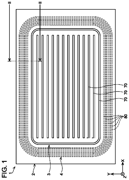
FIG. 1 is an external view of a semiconductor package which includes a nitride semiconductor device according to a preferred embodiment of the present invention.
FIG. 2 is a schematic cross-sectional view of the nitride semiconductor device.
FIGS. 3A to 3C are diagrams for illustrating how to measure a value of N.sub.A+N.sub.DA−N.sub.D−N.sub.DD.
FIGS. 4A and 4B are diagrams for illustrating how to measure a value of N.sub.AN.sub.DA−N.sub.D−N.sub.DD in a semi-insulating GaN layer.
FIG. 5 is a diagram for illustrating I-V characteristics of FIGS. 4A and 4B .
FIG. 6 is a graph showing a relationship between a drain voltage V.sub.D and an output capacity C.sub.OSS.
FIG. 7 is a diagram for illustrating how to determine a depletion voltage of a two-dimensional electron gas under a field plate.
FIG. 8 is a diagram for illustrating how to determine a depletion voltage of the two-dimensional electron gas in a region from an end of the field plate to a drain.
FIG. 9 is a diagram for illustrating the dependence of a current on a trap concentration.
FIGS. 10A to 10C are energy band diagrams showing the movement of electrons over time until a current starts to flow.
FIG. 11 is a simulation result showing the potential distribution of a nitride semiconductor device according to a reference example.
FIG. 12 is a simulation result showing the current density of the nitride semiconductor device according to the reference example.
FIG. 13 is a simulation result showing the trap occupancy rate of the nitride semiconductor device according to the reference example.
FIG. 14 is a simulation result showing the potential distribution of the nitride semiconductor device according to the preferred embodiment of the present invention.
FIG. 15 is a simulation result showing the current density of the nitride semiconductor device according to the preferred embodiment of the present invention.
FIG. 16 is a simulation result showing the trap occupancy rate of the nitride semiconductor device according to the preferred embodiment of the present invention.
FIG. 17 is a graph in which leak currents in the present preferred embodiment and the reference example are compared.
FIG. 18 is a diagram showing a relationship between a carbon concentration and N.sub.A+N.sub.DA−N.sub.D−N.sub.DD.
FIG. 19A is a diagram showing a reference structure 1 which is set for simulation.
FIG. 19B is a diagram showing a reference structure 2 which is set for simulation.
FIG. 20A is a diagram showing a relationship between the carbon concentration and the sheet resistance of the two-dimensional electron gas.
FIG. 20B is a diagram showing a relationship between the carbon concentration and the mobility of the two-dimensional electron gas.
FIG. 20C is a diagram showing a relationship between the carbon concentration and the sheet carrier density of the two-dimensional electron gas.
FIG. 21 is a diagram showing a relationship between the sheet carrier density N.sub.S and the mobility (2DEG mobility) of the two-dimensional electron gas.
FIG. 22A is a diagram showing a structure of AlGaN/GaN between a gate and a drain.
FIG. 22B is a diagram showing a structure of AlGaN/GaN in a gate portion.
FIG. 23 is a diagram showing a relationship between a gate length and a gate withstand voltage.
FIG. 24 is a diagram showing a relationship between N.sub.A+N.sub.DA−N.sub.D−N.sub.DD and the depletion voltage under the field plate.
Description of embodiments
In a preferred embodiment of the present invention, a nitride semiconductor device is provided which includes a nitride semiconductor layer having a gate, a source and a drain and a field plate on the nitride semiconductor layer electrically connected to the gate or the source and in which when it is assumed that a drain voltage value where the value of C.sub.OSS is reduced to one half of a value when a drain voltage is 0 V is V.sub.1 (V), the dielectric breakdown voltage of the device is V.sub.2 (V), a gate length is L.sub.g (cm), a field plate length is L.sub.fp (cm), a shallow acceptor concentration is N.sub.A (/cm.sup.3), a deep acceptor concentration is N.sub.DA (/cm.sup.3), a vacuum permittivity is ∈.sub.0 and the relative permittivity of the nitride semiconductor layer is ∈, formulas
and
below are satisfied. V .sub.1 <q ( N .sub.A +N .sub.DA).Math. L .sub.g.sup.2/2∈.sub.0∈
V .sub.2 <q ( N .sub.A +N .sub.DA).Math.( L .sub.g +L .sub.fp).sup.2/2∈.sub.0∈
In this case, the nitride semiconductor device may satisfy formulas
and
below. q ( N .sub.A +N .sub.DA).Math. L .sub.g.sup.2/2∈.sub.0∈<1.2 V .sub.1
q ( N .sub.A +N .sub.DA).Math.( L .sub.g +L .sub.fp).sup.2/2∈.sub.0∈<1.2 V .sub.2
In a preferred embodiment of the present invention, a nitride semiconductor device is provided which includes a nitride semiconductor layer having a gate, a source and a drain and a field plate on the nitride semiconductor layer electrically connected to the gate or the source and in which when it is assumed that a drain voltage value where the value of C.sub.OSS is reduced to one half of a value when a drain voltage is 0 V is V.sub.1 (V), the dielectric breakdown voltage of the device is V.sub.2 (V), a gate length is L.sub.g (cm), a field plate length is L.sub.fp (cm), a shallow donor concentration is N.sub.D (/cm.sup.3), a deep donor concentration is N.sub.DD (/cm.sup.3), a shallow acceptor concentration is N.sub.A (/cm.sup.3), a deep acceptor concentration is N.sub.DA (/cm.sup.3), a vacuum permittivity is ∈.sub.0 and the relative permittivity of the nitride semiconductor layer is ∈, formulas
and
below are satisfied. V .sub.1 <q ( N .sub.A +N .sub.DA −N .sub.D −N .sub.DD).Math. L .sub.g.sup.2/2∈.sub.0∈
V .sub.2 <q ( N .sub.A +N .sub.DA −N .sub.D −N .sub.DD).Math.( L .sub.g +L .sub.fp).sup.2/2∈.sub.0∈
In this case, the nitride semiconductor device may satisfy formulas
and
below. q ( N .sub.A +N .sub.DA −N .sub.D −N .sub.DD).Math. L .sub.g.sup.2/2∈.sub.0∈<1.2 V .sub.1
q ( N .sub.A +N .sub.DA −N .sub.D −N .sub.DD).Math.( L .sub.g +L .sub.fp).sup.2/2∈.sub.0∈<1.2 V .sub.2
In a preferred embodiment of the present invention, a nitride semiconductor device is provided which includes a nitride semiconductor layer having a gate, a source and a drain and a field plate on the nitride semiconductor layer electrically connected to the gate or the source and in which when it is assumed that a drain voltage value where the value of C.sub.OSS is reduced to one half of a value when a drain voltage is 0 V is V.sub.1 (V), the maximum rated voltage of the device is V.sub.2 (V), a gate length is L.sub.g (cm), a field plate length is L.sub.fp (cm), a shallow acceptor concentration is N.sub.A (/cm.sup.3), a deep acceptor concentration is N.sub.DA (/cm.sup.3), a vacuum permittivity is ∈.sub.0 and the relative permittivity of the nitride semiconductor layer is ∈, formulas
and
below are satisfied. V .sub.1 <q ( N .sub.A +N .sub.DA).Math. L .sub.g.sup.2/2∈.sub.0∈
V .sub.2 <q ( N .sub.A +N .sub.DA).Math.( L .sub.g +L .sub.fp).sup.2/2∈.sub.0∈
In this case, the nitride semiconductor device may satisfy formulas
and
below. q ( N .sub.A +N .sub.DA).Math. L .sub.g.sup.2/2∈.sub.0∈<1.2 V .sub.1
q ( N .sub.A +N .sub.DA).Math.( L .sub.g +L .sub.fp).sup.2/2∈.sub.0∈<1.2 V .sub.2
In a preferred embodiment of the present invention, a nitride semiconductor device is provided which includes a nitride semiconductor layer having a gate, a source and a drain and a field plate on the nitride semiconductor layer electrically connected to the gate or the source and in which when it is assumed that a drain voltage value where the value of C.sub.OSS is reduced to one half of a value when a drain voltage is 0 V is V.sub.1 (V), the maximum rated voltage of the device is V.sub.2 (V), a gate length is L.sub.g (cm), a field plate length is L.sub.fp (cm), a shallow donor concentration is N.sub.D (/cm.sup.3), a deep donor concentration is N.sub.DD (/cm.sup.3), a shallow acceptor concentration is N.sub.A (/cm.sup.3), a deep acceptor concentration is N.sub.DA (/cm.sup.3), a vacuum permittivity is ∈.sub.0 and the relative permittivity of the nitride semiconductor layer is ∈, formulas
and
below are satisfied. V .sub.1 <q ( N .sub.A +N .sub.DA −N .sub.D −N .sub.DD).Math. L .sub.g.sup.2/2∈.sub.0∈
V .sub.2 <q ( N .sub.A +N .sub.DA −N .sub.D −N .sub.DD).Math.( L .sub.g +L .sub.fp).sup.2/2∈.sub.0∈
In this case, the nitride semiconductor device may satisfy formulas
and
below. q ( N .sub.A +N .sub.DA −N .sub.D −N .sub.DD).Math. L .sub.g.sup.2/2∈.sub.0∈<1.2 V .sub.1
q ( N .sub.A +N .sub.DA −N .sub.D −N .sub.DD).Math.( L .sub.g +L .sub.fp).sup.2/2∈.sub.0∈<1.2 V .sub.2
In a preferred embodiment of the present invention, a nitride semiconductor device is provided which includes a nitride semiconductor layer having a gate, a source and a drain and a field plate on the nitride semiconductor layer electrically connected to the gate or the source and in which when it is assumed that a drain voltage value where the value of C.sub.OSS is reduced to one half of a value when a drain voltage is 0 V is V.sub.1 (V), the sheet carrier density of a two-dimensional electron gas is N.sub.S (/cm.sup.2), a gate length is L.sub.g (cm), a field plate length is L.sub.fp (cm), a shallow donor concentration is N.sub.D (/cm.sup.3), a deep donor concentration is N.sub.DD (/cm.sup.3), a shallow acceptor concentration is N.sub.A(/cm.sup.3), a deep acceptor concentration is N.sub.DA (/cm.sup.3), a vacuum permittivity is ∈.sub.0 and the relative permittivity of the nitride semiconductor layer is ∈, formulas
and
below are satisfied. V .sub.1 <q ( N .sub.A +N .sub.DA −N .sub.D −N .sub.DD).Math. L .sub.g.sup.2/2∈.sub.0∈
N .sub.S.sup.2/( N .sub.A +N .sub.DA −N .sub.D −N .sub.DD)<( N .sub.A +N .sub.DA −N .sub.D −N .sub.DD).Math.( L .sub.g +L .sub.fp).sup.2
In this case, the nitride semiconductor device may satisfy formulas
and
below. q ( N .sub.A +N .sub.DA −N .sub.D −N .sub.DD).Math. L .sub.g.sup.2/2∈.sub.0∈<1.2 V .sub.1
( N .sub.A +N .sub.DA −N .sub.D −N .sub.DD).Math.( L .sub.g +L .sub.fp).sup.2<1.2 N .sub.S.sup.2/( N .sub.A +N .sub.DA −N .sub.D −N .sub.DD)
In a preferred embodiment of the present invention, a nitride semiconductor device is provided which includes a nitride semiconductor layer having a gate, a source and a drain and a field plate on the nitride semiconductor layer electrically connected to the gate or the source and in which when it is assumed that a drain voltage value where the value of C.sub.OSS is reduced to one half of a value when a drain voltage is 0 V is V.sub.1 (V), the sheet carrier density of a two-dimensional electron gas is N.sub.S (/cm.sup.2), a gate length is L.sub.g (cm), a field plate length is L.sub.fp (cm), a shallow acceptor concentration is N.sub.A (/cm.sup.3), a deep acceptor concentration is N.sub.DA(/cm.sup.3), a vacuum permittivity is ∈.sub.0 and the relative permittivity of the nitride semiconductor layer is ∈, formulas
and
below are satisfied. V .sub.1 <q ( N .sub.A +N .sub.DA).Math. L .sub.g.sup.2/2∈.sub.0∈
N .sub.S.sup.2/( N .sub.A +N .sub.DA)<( N .sub.A N .sub.DA).Math.( L .sub.g +L .sub.fp).sup.2
In this case, the nitride semiconductor device may satisfy formulas
and
below. q ( N .sub.A +N .sub.DA).Math. L .sub.g.sup.2/2∈.sub.0∈<1.2 V .sub.1
( N .sub.A +N .sub.DA).Math.( L .sub.g +L .sub.fp).sup.2<1.2 N .sub.S.sup.2/( N .sub.A +N .sub.DA)
In the preferred embodiment of the present invention, the gate length L.sub.g may be equal to or less than 0.5 μm, the field plate length L.sub.fp may be equal to or less than 0.5 μm and the maximum rated voltage of the device may be equal to or more than 50 V.
In the preferred embodiment of the present invention, the nitride semiconductor layer may be doped with at least one type of impurity selected from a group consisting of C, Be, Cd, Ca, Cu, Ag, Au, Sr, Ba, Li, Na, K, Sc, Zr, Fe, Co, Ni, Mg, Ar and He such that a deep acceptor level is formed.
In a preferred embodiment of the present invention, a nitride semiconductor device is provided which includes a nitride semiconductor layer which includes an electron transit layer and an electron supply layer that is in contact with the electron transit layer and that has a composition different from the electron transit layer, a gate, a source and a drain on the nitride semiconductor layer and a field plate on the nitride semiconductor layer electrically connected to the gate or the source and in which at least a part of the electron transit layer contains carbon, and the concentration of the carbon is 1×10.sup.18 cm.sup.−3 to 1×10.sup.19 cm.sup.−3.
In the preferred embodiment of the present invention, the electron transit layer may include a first region that forms an interface between the electron transit layer and the electron supply layer and a second region that is formed in a part 50 nm or more apart from the interface, and the carbon concentration of the second region may be 1×10.sup.18 cm.sup.−3 to 1×10.sup.19 cm.sup.−3, and the carbon concentration of the first region may be equal to or less than 1×10.sup.17 cm.sup.3.
In the preferred embodiment of the present invention, when it is assumed that a shallow donor concentration is N.sub.D (/cm.sup.3), a deep donor concentration is N.sub.DD (/cm.sup.3), a shallow acceptor concentration is N.sub.A (/cm.sup.3) and a deep acceptor concentration is N.sub.DA (/cm.sup.3), N.sub.A+N.sub.DA−N.sub.D−N.sub.DD in the second region of the electron transit layer may be 4×10.sup.16 cm.sup.−3 to 8×10.sup.16 cm.sup.−3.
In a preferred embodiment of the present invention, a nitride semiconductor device is provided which includes: a nitride semiconductor layer which includes an electron transit layer and an electron supply layer that is in contact with the electron transit layer and that has a composition different from the electron transit layer; a gate, a source and a drain on the nitride semiconductor layer; and a field plate which is electrically connected to the gate or the source and which is arranged on the nitride semiconductor layer via an insulating film and in which a gate length L.sub.g is equal to or less than 0.6 μm, at least a part of the electron transit layer contains carbon, the concentration of the carbon is equal to or more than 1×10.sup.18 cm.sup.−3 and when it is assumed that the thickness of the insulating film under the field plate is d, and the relative permittivity of the insulating film is ∈, d/∈≦14 is satisfied.
In the preferred embodiment of the present invention, in a case where when the gate is off, a voltage is applied between the source and the drain, as indicated in formulas
and
described above, a voltage (the right-hand side of each formula) when a region of the nitride semiconductor layer under the gate is punched through is higher than the voltage V.sub.1 (the left-hand side of each formula) when the two-dimensional electron gas disappears. In this way, it is possible to prevent the punch-through under the gate, and it is thus possible to reduce the occurrence of a leak current when the gate is off.
As indicated in formulas (2), (6),
and
described above, a voltage (the right-hand side of each formula) when a region of the nitride semiconductor layer under the field plate is punched through is higher than the dielectric breakdown voltage V.sub.2 or the maximum rated voltage V.sub.2 of the device, and it is thus possible to realize a highly reliable device.
As is clear from each formula, the effect of the enhancement of the withstand voltage and the reliability described above can be realized by adjusting the values (such as the shallow acceptor concentration N.sub.A and the deep acceptor concentration N.sub.DA) of the terms other than the gate length L.sub.g in each formula even if the gate length L.sub.g is reduced. Hence, the gate length L.sub.g is designed to be a desired length, and it is thus also possible to enhance the switching speed of the device while maintaining the withstand voltage.
Preferred embodiments of the present invention will be described in detail below with reference to accompanying drawings.
FIG. 1 is an external view of a semiconductor package 1 which includes a nitride semiconductor device 3 according to a preferred embodiment of the present invention.
The semiconductor package 1 includes a terminal frame 2 , the nitride semiconductor device 3 (chip) and a resin package 4 .
The terminal frame 2 is made of a metal and is formed in the shape of a plate. The terminal frame 2 includes a base portion 5 (island) which supports the nitride semiconductor device 3 , a drain terminal 6 , a source terminal 7 and a gate terminal 8 . The drain terminal 6 is formed integrally with the base portion 5 . The drain terminal 6 , the source terminal 7 and the gate terminal 8 are respectively electrically connected to the drain, the source and the gate of the nitride semiconductor device 3 via bonding wires 9 to 11 . The source terminal 7 and the gate terminal 8 are arranged so as to sandwich the drain terminal 6 in the center.
The resin package 4 is formed of, for example, a known mold resin such as an epoxy resin, and seals the nitride semiconductor device 3 . The resin package 4 covers the base portion 5 of the terminal frame 2 and the bonding wires 9 to 11 together with the nitride semiconductor device 3 . Parts of the three terminals 6 to 8 are exposed from the resin package 4 .
FIG. 2 is a schematic cross-sectional view of the nitride semiconductor device 3 . FIG. 2 does not show a cross section taken in a specific position of FIG. 1 but shows a cross section of a collection of elements necessary for the description of the present preferred embodiment.
The nitride semiconductor device 3 includes a substrate 12 , a buffer layer 13 which is formed on the surface of the substrate 12 , an electron transit layer 14 which is epitaxially grown on the buffer layer 13 and an electron supply layer 15 which is epitaxially grown on the electron transit layer 14 . The nitride semiconductor device 3 further includes a gate insulating film 16 which covers the surface of the electron supply layer 15 and a source electrode 17 and a drain electrode 18 which penetrate contact holes 17 a and 18 a formed in the gate insulating film 16 to make ohmic contact with the electron supply layer 15 and which serve as ohmic electrodes. The source electrode 17 and the drain electrode 18 are arranged with an interval, and a gate electrode 19 is arranged between them. The gate electrode 19 is opposite to the electron supply layer 15 via the gate insulating film 16 .
The substrate 12 may be, for example, a conductive silicon substrate. The conductive silicon substrate may have, for example, an impurity concentration of 1×10.sup.17 cm.sup.−3 to 1×10.sup.20 cm.sup.−3 (more specifically, 1×10.sup.18 cm.sup.−3).
The buffer layer 13 may be a multilayer buffer layer in which a first buffer layer 131 and a second buffer layer 132 are stacked. The first buffer layer 131 is in contact with the surface of the substrate 12 , and the second buffer layer 132 is stacked on the surface of the first buffer layer 131 (the surface on the opposite side of the substrate 12 ). In the present preferred embodiment, the first buffer layer 131 is formed with an AlN film, and the thickness of the film may be, for example, about 0.2 μm. In the present preferred embodiment, the second buffer layer 132 is formed with an AlGaN film, and the thickness of the film may be, for example, about 0.2 μm.
The gate insulating film 16 may be a multilayer gate insulating film in which a first insulating layer 161 and a second insulating layer 162 are stacked. The first insulating layer 161 is in contact with the surface of the electron supply layer 15 , and the second insulating layer 162 is stacked on the surface of the first insulating layer 161 (the surface on the opposite side of the electron supply layer 15 ). In the present preferred embodiment, the first insulating layer 161 is formed with an SiN film, and the thickness of the film may be, for example, about 500 angstroms. The first insulating layer 161 described above can be formed by a plasma CVD (chemical vapor deposition) method, a thermal CVD method, sputtering or the like. In the first insulating layer 161 , an opening 161 a is formed so that the second insulating layer 162 is made to enter so as to make contact with the electron supply layer 15 . In the present preferred embodiment, the second insulating layer 162 is formed of alumina (Al.sub.aO.sub.b), and the thickness of the film may be, for example, about 300 angstroms. The second insulating layer 162 has a concave portion 162 a in a part of the first insulating layer 161 which enters the opening 161 a . The second insulating layer 162 described above can be formed by accurately controlling the thickness of the film such as by an ALD method.
When an alumina film is formed by the ALD method, in general, a variation in the composition ratio of a:b between Al and O is produced, and not all is formed into Al.sub.2O.sub.3. This is because the ALD method is a process of a relatively low temperature. However, even if in an insulator formed of Al and O, its composition is not strictly controlled, an insulating layer having a high band-gap and a high withstand voltage can be formed. In the present specification, the composition is referred to as “alumina” which includes cases where the composition ratio of a:b between Al and O is not 2:3.
The electron transit layer 14 and the electron supply layer 15 are formed of group-III nitride semiconductors having different Al compositions (hereinafter simply referred to as “nitride semiconductors”). For example, the electron transit layer 14 may be formed with a GaN layer, and the thickness thereof may be about 0.5 μm. In the present preferred embodiment, the electron supply layer 15 is formed with an Al.sub.xGa.sub.1-xN layer (0<x<1), and the thickness thereof is, for example, 5 to 30 nm (more specifically, about 20 nm).
As described above, the electron transit layer 14 and the electron supply layer 15 are formed of nitride semiconductors having different Al compositions to form a heterojunction, and a lattice mismatch occurs therebetween. Then, due to polarization caused by the heterojunction and the lattice mismatch, in a position close to an interface between the electron transit layer 14 and the electron supply layer 15 (for example, a position of a distance of about a few angstroms from the interface), a two-dimensional electron gas 20 is spread.
In the electron transit layer 14 , with respect to the energy band structure thereof, a shallow donor level E.sub.D, a deep donor level E.sub.DD, a shallow acceptor level E.sub.A and a deep acceptor level E.sub.DA may be formed.
The shallow donor level E.sub.D is, for example, an energy level in a position 0.025 eV or less away from an energy level E.sub.C of the lower end (bottom) of the conduction band of the electron transit layer 14 , and may be simply referred to as a “donor level E.sub.D” when it is possible to distinguish it from the deep donor level E.sub.DD. In general, donor electrons with which this position is doped are free electrons even at room temperature (thermal energy kT=about 0.025 eV) because they are excited by the conduction band. As an impurity which dopes the GaN electron transit layer 14 to form the shallow donor level E.sub.D, for example, at least one type selected from a group consisting of Si and O is present. On the other hand, the deep donor level E.sub.DD is, for example, an energy level in a position 0.025 eV or more away from the energy level E.sub.C of the lower end (bottom) of the conduction band of the electron transit layer 14 . In other words, the deep donor level E.sub.DD is formed by doping with a donor in which ionization energy necessary for excitation is higher than thermal energy at room temperature. Hence, in general, donor electrons with which this position is doped are not excited by the conduction band at room temperature and are captured by the donor.
The shallow acceptor level E.sub.A is, for example, an energy level in a position 0.025 eV or less away from an energy level E.sub.V of the upper end (top) of the valence electron of the electron transit layer 14 , and may be simply referred to as an “acceptor level E.sub.A” when it is possible to distinguish it from the deep acceptor level E.sub.DA. In general, acceptor holes with which this position is doped are free holes even at room temperature (thermal energy kT=about 0.025 eV) because they are excited by the valence band. On the other hand, the deep acceptor level E.sub.DA is, for example, an energy level in a position 0.025 eV or more away from the energy level E.sub.V of the upper end (top) of the valence electron of the electron transit layer 14 . In other words, the deep acceptor level E.sub.DA is formed by doping with an acceptor in which ionization energy necessary for excitation is higher than thermal energy at room temperature. Hence, in general, acceptor holes with which this position is doped are not excited by the valence band at room temperature and are captured by the acceptor. Although at room temperature, as an impurity which generates holes, Mg is known, its activation rate (ratio of generated holes to the amount of doping) is 1/10 or less, and thus Mg can be interpreted as a shallow acceptor or a deep acceptor but in the present invention, since N.sub.A+N.sub.DA is an important value, Mg may be interpreted as either of them. Examples of an impurity which dopes the electron transit layer 14 made of GaN so as to form the deep acceptor level E.sub.DA include at least one type selected from a group consisting of, for example, C, Be, Cd, Ca, Cu, Ag, Au, Sr, Ba, Li, Na, K, Sc, Zr, Fe, Co, Ni, Mg, Ar and He.
In the present preferred embodiment, the concentrations of impurities (dopants) which form the shallow donor level E.sub.D, the deep donor level E.sub.DD, the shallow acceptor level E.sub.A and the deep acceptor level E.sub.DA described above are respectively referred to as a shallow donor concentration N.sub.D, a deep donor concentration N.sub.DD, a shallow acceptor concentration N.sub.A and a deep acceptor concentration N.sub.DA.
The impurity concentration of the electron transit layer 14 as a whole preferably satisfies N.sub.A+N.sub.DA−N.sub.D−N.sub.DD>0. The inequality means that as compared with the total sum (N.sub.D+N.sub.DD, hereinafter the total sum may also be referred to as a donor concentration N.sub.d) of the impurity concentrations of donor atoms which can discharge electrons, the total sum (N.sub.A+N.sub.DA, hereinafter the total sum may also be referred to as a trap concentration N.sub.t) of the impurity concentrations of acceptor atoms which can capture the discharged electrons is large. In other words, since in the electron transit layer 14 , almost all of the electrons discharged from the shallow donor atoms and the deep donor atoms are not excited by the conduction band and are captured by the shallow acceptor atoms or the deep acceptor atoms, the electron transit layer 14 is formed of a semi-insulating i-type GaN.
However, even when the layer is doped with at least one type of impurity selected from a group consisting of C, Be, Cd, Ca, Cu, Ag, Au, Sr, Ba, Li, Na, K, Sc, Zr, Fe, Co, Ni, Mg, Ar and He, not all of the impurity functions as the deep acceptor, and for example, in the case of C (carbon), the impurity functions as the deep acceptor by being replaced into an N (nitrogen) site in a Group III nitride semiconductor crystal whereas the impurity functions as the shallow donor by being replaced into a Group III element site. The proportions of the replacements into the individual sites depend on the concentration of the carbon with which the layer is doped. The layer is doped with the impurity, and a crystal defect is thus produced but it is not clear which one of the shallow donor, the deep donor, the shallow acceptor and the deep acceptor the crystal defect functions as. Hence, it is impossible to find the value of N.sub.A+N.sub.DA−N.sub.D−N.sub.DD with the measurement of the impurity concentration by SIMs (Secondary Ion Mass Spectrometry).
It is found that the measurement of the value of N.sub.A+N.sub.DA−N.sub.D−N.sub.DD can be performed by measurement of a leak current in the longitudinal direction of a semi-insulating layer as shown in FIG. 3A . As described above, the electron transit layer is the semi-insulating layer in which the electrons discharged from the shallow donor and the deep donor are captured by the shallow acceptor and the deep acceptor. As shown in FIG. 10A , these layers are in a state in which without any bias, a deep acceptor level where no electron is captured is present and an empty deep acceptor is present. Here, the GaN layer is electrically neutral. As shown in FIG. 10B , since under an external voltage of a certain value or less, an electron is captured by the deep acceptor which captures no electron without any bias, and the positive bias side is thus negatively charged to cancel out the electric field, an extremely small current flows. Here, a region of the semi-insulating layer on the positive bias side is negatively charged, and the charge density thereof is N.sub.A+N.sub.DA−N.sub.D−N.sub.DD. When a voltage of a certain value or more is applied, electrons are captured by all the deep acceptor levels, the electric field cannot be cancelled out anymore and the current starts to be increased. Here, all the regions of the semi-insulating layer are negatively charged, and the charge density thereof is N.sub.A+N.sub.DA−N.sub.D−N.sub.DD. Hence, when the distribution of N.sub.A+N.sub.DA−N.sub.D−N.sub.DD in the semi-insulating layer is uniform, and it is assumed that an elementary charge amount is q, the thickness of the semi-insulating layer is d and a voltage when the current starts to be increased is V.sub.TH, Poisson's equation is used, and it is thus possible to determine N.sub.A+N.sub.DA−N.sub.D−N.sub.DD by the formula of N.sub.A+N.sub.DA−N.sub.D−N.sub.DD=2∈∈.sub.0V.sub.TH/qd.sup.2.
In the measurement, as shown in FIGS. 3B and 3C , in the semi-insulating layer, electrodes may be formed through a conductive layer and a conductive substrate.
When GaN is grown on different types of substrates, it is necessary to introduce a buffer layer between the GaN and the substrate. For example, in the case of a semi-insulating GaN on a Si substrate, between the conductive substrate and the semi-insulating GaN layer which is a measurement target, a semi-insulating buffer layer formed with the stacked layers of AlN and AlGaN is included. Since it is expected that these buffer layers have N.sub.A+N.sub.DA−N.sub.D−N.sub.DD which differs from the semi-insulating GaN layer, in order for N.sub.A+N.sub.DA−N.sub.D−N.sub.DD of the semi-insulating GaN layer to be measured, as shown in FIGS. 4A and 4B , a sample grown to the buffer layer and a sample grown to the semi-insulating GaN layer are prepared, and a positive bias is applied to the electrode on the substrate. When it is assumed that in each sample, the difference of V.sub.TH of each sample is ΔV.sub.TH, the thickness of the semi-insulating GaN layer is d.sub.GaN and the thickness of the buffer layer is d.sub.buffer, it is possible to determine N.sub.A+N.sub.DA−N.sub.D−N.sub.DD by the formula of N.sub.A+N.sub.DA−N.sub.D−N.sub.DD=2∈∈.sub.0ΔV.sub.TH/q (d.sub.GaN.sup.2+2d.sub.GaNd.sub.buffer).
For example, when the thickness of the semi-insulating GaN layer which is grown under certain conditions is 1.5 μm, and the thickness of the buffer layer is 0.2 μm, the I-V characteristic shown in FIG. 5 is obtained, and N.sub.A+N.sub.DA−N.sub.D−N.sub.DD of the semi-insulating GaN layer can be determined to be 3.2×10.sup.16/cm.sup.3.
The electron supply layer 15 may have, in the interface with the electron transit layer 14 , an AlN layer which has about a thickness of a few atoms (equal to or less than 5 nm, preferably 1 to 5 nm and more preferably 1 to 3 nm). The AlN layer described above reduces the scattering of electrons and facilitates the enhancement of electron mobility.
The gate electrode 19 may be formed with a multilayer electrode film which has a lower layer in contact with the gate insulating film 16 and an upper layer stacked on the lower layer. The lower layer may be formed of Ni, Pt, Mo, W or TiN, and the upper layer may be formed of Au or Al. The gate electrode 19 is arranged so as to be displaced to the source electrode 17 , and thereby has an asymmetric structure in which the distance between the gate and the drain is longer than the distance between the gate and the source. The asymmetric structure alleviates a high electric field produced between the gate and the drain to facilitate the enhancement of the withstand voltage.
The gate electrode 19 includes a gate main body portion 191 which is formed in the second insulating layer 162 between the source electrode 17 and the drain electrode 18 and which enters the concave portion 162 a and a field plate portion 192 which is continuous to the gate main body portion 191 and which is extended on the gate insulating film 16 outside the opening 161 a toward the drain electrode 18 . A distance L.sub.fp from a drain end 191 a which is an end portion on the side of the drain electrode 18 in the interface between the gate main body portion 191 and the second insulating layer 162 to an end portion of a field plate portion 192 on the side of the drain electrode 18 is referred to as a field plate length. On the other hand, a distance L.sub.g from the drain end 191 a in the interface between the gate main body portion 191 and the second insulating layer 162 to a source end 191 b which is an end portion on the side of the source electrode 17 is referred to as a gate length. In other words, the width of an effective gate area (region within the concave portion 162 a ) which is a contact area between the gate electrode 19 and the bottom surface of the concave portion 162 a of the second insulating layer 162 is referred to as the gate length. Furthermore, in the present specification, a distance between the gate main body portion 191 and the drain electrode 18 is represented by L.sub.gd.
The field plate length L.sub.fp is preferably equal to or more than one tenth but equal to or less than one half of the distance L.sub.gd between the gate and the drain. Specifically, it may be equal to or more than 0.1 μm but equal to or less than 0.5 μm. On the other hand, the gate length L.sub.g is preferably equal to or more than 0.1 μm but equal to or less than 1.0 μm. Specifically, it may be equal to or more than 0.2 μm but equal to or less than 0.5 μm.
The source electrode 17 and the drain electrode 18 are, for example, ohmic electrodes which include Ti and Al, and are electrically connected via the electron supply layer 15 to the two-dimensional electron gas 20 .
The bonding wires 9 to 11 shown in FIG. 1 are connected to the drain electrode 18 , the source electrode 17 and the gate electrode 19 , respectively. On the back surface of the substrate 12 , a back surface electrode 21 is formed, and the substrate 12 is connected via the back surface electrode 21 to the base portion 5 . Hence, in the present preferred embodiment, the substrate 12 is electrically connected via the bonding wire 9 to the drain electrode 18 so as to have a drain potential.
In the nitride semiconductor device 3 , on the electron transit layer 14 , the electron supply layer 15 having a different Al composition is formed so as to form a hetero junction. In this way, within the electron transit layer 14 in the vicinity of the interface between the electron transit layer 14 and the electron supply layer 15 , the two-dimensional electron gas 20 is formed, and a HEMT which utilizes the two-dimensional electron gas 20 as a channel is formed. The gate electrode 19 is opposite to the electron supply layer 15 through the gate insulating film 16 . An appropriate negative voltage is applied to the gate electrode 19 , and thus the channel formed with the two-dimensional electron gas 20 can be interrupted. Hence, a control voltage is applied to the gate electrode 19 , and it is thus possible to turn on and off the region between the source and the drain.
In use, for example, between the source electrode 17 and the drain electrode 18 , a predetermined voltage (for example, 200 to 600 V) in which the side of the drain electrode 18 is positive is applied. In this state, an off-voltage (for example, −5 V) or an on-voltage (for example, 0 V) is applied to the gate electrode 19 under the assumption that the source electrode 17 has a reference potential (0 V).
In order to enhance the withstand voltage in the nitride semiconductor device 3 which is operated as described above, the nitride semiconductor device 3 satisfies formula
or
below. V .sub.1 <q ( N .sub.A +N .sub.DA).Math. L .sub.g.sup.2/2∈.sub.0∈
V .sub.1 <q ( N .sub.A +N .sub.DA −N .sub.D −N .sub.DD).Math. L .sub.g.sup.2/2∈.sub.0∈
In formulas
and
described above, ∈.sub.0 is a vacuum permittivity, and ∈ is the relative permittivity of the electron transit layer 14 (GaN). V.sub.1 on the left-hand side of each of formulas
and
represents a voltage when the electron transit layer 14 under the field plate portion 192 is depleted and in such a region, the two-dimensional electron gas 20 is depleted. On the other hand, the right-hand side of each of formulas
and
represents a voltage when punch-through occurs under the gate and thus a leak current starts to flow. In other words, the inequalities represented by formulas
and
The description continues in the full USPTO document.
 Lapsed, fee not paid17 drawings

