 Lapsed, fee not paid6 drawings
Cameras, Displays & Optics · US 9,865,189 B2
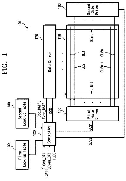
Display device having power saving glance mode
An example processing system for a display device includes driver circuitry and a control circuit.
US 9,865,199 B2 · Assignee: Funai Electric Co., Ltd. · Inventors: Kita; Tatsuya et al.
Sheet 1 of 24 from the published document. All sheets in the USPTO PDF
A backlight drive circuit supplies drive current to a plurality of backlights, each of the backlights is extinguished before a signal voltage is written to a liquid crystal pixel group of a line corresponding to the backlight, each drive current in the lit period of each of the backlights is a first current when the adjustment value is a first adjustment value and a second current whose current value is higher than the first current when the adjustment value is a second adjustment value that is lower than the first adjustment value, and the lighting duty ratio to obtain a given luminance using the second current is smaller than the lighting duty ratio to obtain the luminance using the first current.
Liquid crystal display devices such as liquid crystal televisions have been getting bigger. However, the problem is that as they grow larger, blurring of images when moving pictures are displayed (hereinafter may also be referred to as “motion blur”) becomes more conspicuous. Backlight scanning is a known method in liquid crystal display devices to suppress this motion blur. Backlight scanning refers to lighting and extinguishing a plurality of backlights installed for groups of liquid crystal pixels in a display panel in sequence in the line direction. Such backlight scanning methods include methods of suppressing motion blur by reducing the lighting duty ratio, which is the proportion of the lit period within the backlight flashing cycle, when screen images are moving quickly, while maintaining the lighting duty ratio and suppressing peak current when screen images are moving slowly, t
1 of 24 drawing sheets so far from the published document, cropped to the drawing. Every sheet is in the USPTO PDF.
What the patent claimed, word for word. All of it is now free to use.
The present invention relates to a backlight drive circuit connected to a liquid crystal panel including groups of liquid crystal pixels disposed in a matrix and a plurality of backlights respectively provided so as to correspond to the plurality of lines of the liquid crystal pixel groups.
Liquid crystal display devices such as liquid crystal televisions have been getting bigger. However, the problem is that as they grow larger, blurring of images when moving pictures are displayed (hereinafter may also be referred to as “motion blur”) becomes more conspicuous.
Backlight scanning is a known method in liquid crystal display devices to suppress this motion blur. Backlight scanning refers to lighting and extinguishing a plurality of backlights installed for groups of liquid crystal pixels in a display panel in sequence in the line direction.
Such backlight scanning methods include methods of suppressing motion blur by reducing the lighting duty ratio, which is the proportion of the lit period within the backlight flashing cycle, when screen images are moving quickly, while maintaining the lighting duty ratio and suppressing peak current when screen images are moving slowly, thus suppressing power consumption (for example, see Japanese Patent Application Laid-Open Publication No. 2011-232535).
These methods can serve the dual function of suppressing motion blur and cutting power consumption.
With such a backlight scan system, the lighting duty ratio must be raised when increasing the screen image luminance, i.e., when increasing the backlight luminance.
However, in the method disclosed in the Japanese Patent Application Laid-Open Publication No. 2011-232535, the lighting duty ratio is decreased when screen images are moving quickly, so screen image luminance cannot be increased. In other words, the issue is that when screen images are bright, motion blur cannot be suppressed.
Preferred embodiments of the present invention provide a backlight drive circuit that significantly reduces motion blur even when screen image luminance is high.
A backlight drive circuit according to a preferred embodiment of the present invention is a backlight drive circuit which supplies drive current to a plurality of backlights that are arranged to correspond to a plurality of lines of liquid crystal pixel groups disposed in a matrix, wherein the backlight drive circuit supplies the drive current such that the higher an adjustment value, which indicates a luminance of the backlights, the larger the lighting duty ratio, which is a proportion of the lit period within the flashing cycle of each backlight, the liquid crystal pixel groups transmit, at a transmittance in accordance with the signal voltage written in each liquid crystal pixel, the light from the backlight corresponding to the liquid crystal pixel, the backlight drive circuit extinguishes each backlight before the signal voltage is written to the liquid crystal pixel group of the line corresponding to this backlight, each drive current in the lit period is a first current when the adjustment value is a first adjustment value and a second current whose current value is higher than the first current when the adjustment value is a second adjustment value that is lower than the first adjustment value, and the lighting duty ratio to obtain a given luminance using the second current is smaller than the lighting duty ratio to obtain the luminance using the first current.
Thus, when the adjustment value is the second adjustment value, the lighting duty ratio becomes even smaller. Therefore, motion blur is significantly reduced even when screen image luminance is high. Furthermore, double-imaging is also significantly reduced or prevented by extinguishing the corresponding backlight before writing the signal voltage.
For example, the backlight drive circuit preferably includes a timing instruction unit which orders the lighting and extinguishing timing of each backlight such that the higher the adjustment value, the longer the lit period, a voltage generating unit which generates a first voltage when the adjustment value is above a threshold value and generates a second voltage that is higher than the first voltage when the adjustment value is at or below the threshold value, and backlight drivers which are arranged to correspond to the respective backlights and supply the drive current to the corresponding backlights, and each of the backlight drivers convert the first voltage generated by the voltage generating unit into the first current, convert the second voltage into the second current, and supply the converted currents as the drive current during a period during which the corresponding backlight is ordered to be lit by the timing instruction unit.
As a result, current is switched between two levels with a simple constitution.
Moreover, the timing instruction unit preferably generates a voltage switching signal that indicates whether or not the adjustment value is higher than the threshold value, and the voltage generating unit preferably generates the first voltage when the voltage switching signal generated by the timing instruction unit indicates that the adjustment value is higher than the threshold value and preferably generates the second voltage when the signal indicates that the adjustment value is at or below the threshold value.
In addition, the current value of each of the drive currents during the lit period may be higher as the adjustment value is lower.
As a result, flicker is controlled.
Furthermore, the backlight drive circuit preferably includes a timing instruction unit which orders the lighting and extinguishing timing of each backlight such that the higher the adjustment value, the longer the lit period, a voltage generating unit which generates a voltage that is higher the lower the adjustment value is, and backlight drivers which are arranged to correspond to the respective backlights and supply the drive current to the corresponding backlights, and each of the backlight drivers preferably convert the voltage generated by the voltage generating unit into a current and supply the converted current as the drive current during a period during which the corresponding backlight is ordered to be lit by the timing instruction unit.
Consequently, current is steplessly adjusted with a simple constitution.
Moreover, the timing instruction unit preferably generates a pulse width modulation (PWM) signal which has a duty ratio that is smaller as the adjustment value is lower, and the voltage generating unit preferably includes a digital/analog (D/A) converter which generates an analog voltage that is lower the smaller the duty of the PWM signal is by D/A converting the duty ratio of the PWM signal and an inverter circuit which generates a voltage that is higher the smaller the duty of the PWM signal is by inverting the voltage level of the analog voltage generated by the D/A converter.
In addition, the D/A converter may be an integrator including resistors and capacitors, and the inverter circuit preferably includes a transistor which is configured such that an analog voltage generated by the D/A converter is applied to its control terminal and one of the two output terminals is grounded.
Furthermore, the plurality of adjustment values may also be specified by a user operation.
Moreover, the backlight drive circuit according to another preferred embodiment of the present invention is a backlight drive circuit which supplies drive current to a plurality of backlights that correspond to a plurality of lines of liquid crystal pixel groups disposed in a matrix, wherein the backlight drive circuit supplies the drive current such that the higher an adjustment value, which indicates a luminance of the backlights, the larger a lighting duty ratio, which is a proportion of the lit period within a flashing cycle of each backlight, each drive current in the lit period is a first current when the adjustment value is a first adjustment value and a second current whose current value is higher than the first current when the adjustment value is a second adjustment value that is lower than the first adjustment value, and the lighting duty ratio to obtain a given luminance using the second current is smaller than the lighting duty ratio to obtain the luminance using the first current.
With various preferred embodiments of the present invention, it is possible to realize a backlight drive circuit that significantly reduces or prevents motion blur even when screen image luminance is high.
The above and other elements, features, steps, characteristics and advantages of the present invention will become more apparent from the following detailed description of the preferred embodiments with reference to the attached drawings.
FIG. 1 is a block diagram showing the constitution of a liquid crystal display device in which the backlight drive circuit according to Preferred Embodiment 1 of the present invention is mounted.
FIG. 2 is a block diagram showing the detailed constitution of the backlight drive circuit.
FIG. 3 is a circuit diagram showing one example of the detailed constitution of the voltage switching circuit.
FIG. 4 is a timing chart showing in model form one example of the lighting and extinguishing timing of the backlight panel and the write timing of the signal voltage to the liquid crystal panel in Preferred Embodiment 1 of the present invention.
FIG. 5 is a graph showing drive current during the lit periods of the backlights with respect to the adjustment value.
FIG. 6 is a graph showing the lighting duty ratios of the backlights with respect to the adjustment values.
FIG. 7 is a timing chart showing in model form the lighting and extinguishing timing of the backlight panel and the write timing of the signal voltage to the liquid crystal panel in a comparative example for Preferred embodiment 1.
FIG. 8 is a timing chart showing in model form another example of the lighting and extinguishing timing of the backlight panel and the write timing of the signal voltage to the liquid crystal panel in Preferred Embodiment 1 of the present invention.
FIG. 9 is a table presenting the lighting duty ratios, drive currents, and light emission luminance of the backlight panel when the adjustment value is changed.
FIG. 10 is a graph showing light emission luminance with respect to the adjustment values presented in FIG. 9 .
FIGS. 11A and 11B are graphs showing the chromaticity of the backlight panel when the adjustment value is changed.
FIG. 12 is a block diagram showing the detailed constitution of the backlight drive circuit according to a modified example of Preferred Embodiment 1 of the present invention.
FIG. 13 is a block diagram showing the detailed constitution of the backlight drive circuit according to Preferred Embodiment 2 of the present invention.
FIG. 14 is a circuit diagram showing one example of the detailed constitution of the D/A converting unit.
FIG. 15 is a graph showing drive current during the lit periods of the backlights with respect to the adjustment value.
FIG. 16 is a graph showing the lighting duty ratios of the backlights with respect to the adjustment values.
FIG. 17 is a table presenting the lighting duty ratios, drive currents, and light emission luminance of the backlight panel when the adjustment value is changed.
FIG. 18 is a graph showing light emission luminance with respect to the adjustment values presented in FIG. 17 .
FIGS. 19A and 19B are graphs showing the chromaticity of the backlight panel when the adjustment value is changed.
FIG. 20 is a block diagram showing the detailed constitution of the backlight drive circuit according to a modified example of Preferred Embodiment 2 of the present invention.
FIG. 21 is a timing chart showing in model form the lighting and extinguishing timing of the backlight panel and the write timing of the signal voltage to the liquid crystal panel in the liquid crystal display device according to Comparative Example 1.
FIG. 22 is a timing chart showing in model form the lighting and extinguishing timing of the backlight panel and the write timing of the signal voltage to the liquid crystal panel in the liquid crystal display device according to Comparative Example 2.
FIG. 23 is a graph showing the lighting duty ratio with respect to the adjustment value of the liquid crystal display device according to Comparative Example 2.
FIGS. 24A and 24B are diagrams that illustrate motion blur, wherein FIG. 24A is a diagram indicating a case of a large lighting duty ratio, and FIG. 24B is a diagram indicating a case of a small lighting duty ratio.
First, before describing preferred embodiments of the present invention, the principle of double-imaging and motion blur that occur when moving pictures are displayed in a liquid crystal display device will be described using comparative examples. Comparative Example 1
The principle of double-imaging that occurs in a liquid crystal display device will be described first. FIG. 21 is a timing chart showing in model form the lighting and extinguishing timing of the backlight panel and the write timing of the signal voltage to the liquid crystal panel in the liquid crystal display device according to Comparative Example 1.
This liquid crystal display device includes a liquid crystal panel composed of liquid crystal pixel groups disposed in a matrix, a plurality of backlights provided so as to respectively correspond to the plurality of lines of the liquid crystal pixel groups, and a backlight drive circuit that drives the plurality of backlights.
The scan signal is written to the liquid crystal pixel groups by a gate driver that drives the top portion of the liquid crystal panel, a gate driver that drives the center portion of the liquid crystal panel, and a gate driver that drives the bottom portion of the liquid crystal panel. Each gate driver writes a signal voltage corresponding to the scan signal, which is digital data, to the liquid crystal panel. Here, writing a signal voltage to the liquid crystal panel refers to applying the signal voltage to the liquid crystal pixel groups that constitute the liquid crystal panel.
The plurality of backlights preferably are defined by light emitting diodes (LEDs), for example, and include LEDs arranged to correspond to the top portion of the liquid crystal panel (top LEDs), LEDs provided so as to correspond to the center portion of the liquid crystal panel (center LEDs), and LEDs arranged to correspond to the bottom portion of the liquid crystal panel (bottom LEDs).
The backlight drive circuit is equipped with a plurality of backlight drivers that drive the respective backlights and supplies the backlights with drive current that makes these backlights light during the lit periods of the backlights. During the high period of a scan signal PWM 0 , it supplies a drive current to the LEDs arranged to correspond to the top portion of the liquid crystal panel, during the high period of a scan signal PWM 1 , it supplies a drive current to the LEDs provided so as to correspond to the center portion of the liquid crystal panel, and during the high period of a scan signal PWM 2 , it supplies a drive current to the LEDs provided so as to correspond to the bottom portion of the liquid crystal panel.
Note that the lighting duty ratio is 100% in Comparative Example 1. That is, the scan signals PWM 0 to PWM 2 are always high, and the respective backlights are always lit.
The operation of the liquid crystal display device according to Comparative Example 1 will be described below.
When the gate driver start signal STV (which is a signal that indicates the timing for writing scan signals to the first line of the liquid crystal pixel group) rises, the liquid crystal display device writes the signal voltage to the liquid crystal panel by driving the various gate drivers in sequence.
The liquid crystal pixel line where the signal voltage is written transmits an amount of light in keeping with the signal voltage of the next frame, requiring an amount of time in keeping with the response speed of the liquid crystal pixels. Thus, the liquid crystal display device displays an image according to the scan signal of the next frame.
However, with such a liquid crystal display device, when the signal voltage is rewritten between the previous frame and the next frame, problematic blur can arise due to superimposition of images or the response speed of the liquid crystal. The plurality of backlights are on all the time because the lighting duty ratio is 100%, so these liquid crystal pixels transmit light from the backlights even during the response period of the liquid crystal pixels after the signal voltage is rewritten. Specifically, when the signal voltage is rewritten, the images of the pre-rewriting frame and the post-rewriting frame are displayed. In other words, a double image is displayed. Comparative Example 2
In light of this, in order to suppress such double-imaging on the liquid crystal display device, a constitution is conceivable in which the lighting duty ratio is lowered, and when the signal voltage is rewritten, the corresponding backlight is extinguished.
FIG. 22 is a timing chart showing in model form the lighting and extinguishing timing of the backlight panel and the write timing of the signal voltage to the liquid crystal panel in the liquid crystal display device according to Comparative Example 2. Note that for the sake of simplicity of description, the description will assume that the response time of the liquid crystal pixels is zero in this comparative example.
As shown in FIG. 22 , the liquid crystal display device according to Comparative Example 2 extinguishes the corresponding backlight at the write timing of the next scan signal. It makes the ON duty of the scan signals PWM 0 to PWM 2 equal to about ⅔ (approximately 67%), and during rewriting of the signal voltages of the liquid crystal pixels, it makes the scan signals PWM 0 to PWM 2 low, thus extinguishing the corresponding backlights.
Consequently, double-imaging when signal voltages are rewritten is suppressed. Note that in the description, the response time of the liquid crystal pixels was zero. However, when the response time of the liquid crystal pixels is not zero, motion blur during the response time of the liquid crystal pixels is also suppressed by extinguishing the corresponding backlight during the response time of the liquid crystal pixels as well.
FIG. 23 is a graph showing the lighting duty ratio with respect to the adjustment value of the liquid crystal display device according to Comparative Example 2. Note that the “adjustment value” refers to a value that indicates the luminance of the backlights; the higher the adjustment value, the greater the luminance.
As shown in this figure, the higher the adjustment value, the higher the lighting duty ratio is because the backlights must emit light at a higher luminance. On the other hand, the lower the adjustment value, the lower the lighting duty ratio because the backlights can emit light at a lower luminance.
Here, the backlight of the liquid crystal display device according to Comparative Example 2 has a three-level constitution, and when the vertical scan period is Vs, the response speed of the liquid crystal pixel is, for example, ⅓ Vs.
With such a liquid crystal display device according to Comparative Example 2, double-imaging is suppressed by setting the lighting duty ratio at about ⅓ (approximately 33%) and extinguishing the backlight when signal voltages of liquid crystal pixels are rewritten and during the liquid crystal pixel response period. That is, double-imaging is suppressed with adjustment values which are such that the lighting duty ratio can be kept at or below about 33%. In other words, when the adjustment value results in a lighting duty ratio that exceeds about 33%, double-imaging suppressing effects will not be adequately manifested.
However, the only adjustment values that can make the lighting duty ratio about 33% or below are 0, 1, and 2. At other adjustment values (adjustment values of 3 or higher), the lighting duty ratio will be higher than about 33%, making double-imaging difficult to control. That is, it is difficult to suppress double-imaging in regions of high backlight luminance that result in adjustment values of 3 or higher.
Furthermore, because liquid crystal pixels use a hold drive, there are also problems of motion blur that is generated by retinal afterimages even when liquid crystal response times are shortened.
This motion blur can also be ameliorated by reducing the lighting duty ratio in a manner similar to the method of suppressing double-imaging described above.
FIGS. 24A and 24B are diagrams that illustrate motion blur, wherein FIG. 24A is a diagram indicating a case of a high lighting duty ratio, and FIG. 24B is a diagram indicating a case of a low lighting duty ratio.
As a comparison between FIGS. 24A and 24B makes clear, a smaller lighting duty ratio shown in FIG. 24B reduces motion blur. That is, the more the lighting duty ratio is reduced and backlight lighting brought closer to impulse-style lighting, the more motion blur is suppressed.
Thus, motion blur is suppressed by reducing the lighting duty ratio.
However, as shown in FIG. 23 , reducing the lighting duty ratio results in lower backlight luminance. That is, it is difficult to apply methods that reduce the lighting duty ratio in order to suppress motion blur when backlights are putting out high luminance.
Thus, with the liquid crystal display devices according to Comparative Examples 1 and 2, there is a problem in that it is difficult to suppress double-imaging or motion blur when the backlights emit light at high luminance.
In order to solve such issues, the backlight drive circuits according to the various preferred embodiments of the present invention supply the following sorts of drive currents to each backlight. Namely, as the drive currents for the lit period of each backlight, the backlight drive circuits according to the various preferred embodiments of the present invention supply a first current when the adjustment value is a first adjustment value and supply a second current that has a higher current value than the first current when the adjustment value is a second adjustment value that is lower than the first adjustment value. Moreover, the lighting duty ratio to obtain a given luminance using the second current is smaller than the lighting duty ratio to obtain this same luminance using the first current.
Thus, the backlight drive circuit according to each of the preferred embodiments of the present invention makes the lighting duty ratio even smaller when the adjustment value is the second adjustment value. Accordingly, motion blur is suppressed even when the luminance of screen images is high. In addition, double-imaging also is suppressed by turning off the corresponding backlight before writing the signal voltage.
Preferred embodiments of the present invention will be described in detail below with reference to drawings. Note that the preferred embodiments described below are each for illustrating specific preferred examples of the present invention. The numerical values, shapes, materials, constituent elements, the disposed positions and connection formats of the constituent elements, and so forth shown in the preferred embodiments described below are just examples that do not limit the present invention. The present invention is specified by the scope of the claims. Therefore, those constituent elements not recited in the independent claims that are among the constituent elements in the preferred embodiments described below are not necessarily required in the present invention but are described as constituting a more preferable form.
The backlight drive circuits according to the preferred embodiments of the present invention drive a plurality of backlights that correspond to a plurality of lines of liquid crystal pixel groups disposed in a matrix, and they are included in televisions, for example. Preferred Embodiment 1
The backlight drive circuit according to Preferred Embodiment 1 of the present invention is a backlight drive circuit that supplies drive current to a plurality of backlights, and it makes the lighting duty ratio (which is the proportion of the lit period within the flashing cycle of each backlight) larger as the adjustment value (which indicates the backlight luminance) is higher, and extinguishes each backlight before writing the signal voltage to the corresponding liquid crystal pixel group. Here, the backlight drive circuit supplies, during the lit period, a first current when the adjustment value exceeds a threshold value and supplies a second current that has a greater amperage than the first current when the adjustment value is at or below the threshold value. Furthermore, the lighting duty ratio to obtain a given luminance using the second current is made smaller than the lighting duty ratio to obtain this same luminance using the first current.
Consequently, the backlight drive circuit according to Preferred Embodiment 1 of the present invention suppresses double-imaging and motion blur even when the backlight emits light at high luminance.
The constitution of the backlight drive circuit according to Preferred Embodiment 1 of the present invention will be described below.
FIG. 1 is a block diagram showing the constitution of a liquid crystal display device 200 in which the backlight drive circuit 100 according to Preferred Embodiment 1 of the present invention is mounted.
The liquid crystal display device 200 shown in this figure is a liquid crystal television, for example, including the backlight drive circuit 100 according to Preferred Embodiment 1 of the present invention, a backlight panel 210 , and a liquid crystal panel 220 including liquid crystal pixel groups.
The backlight drive circuit 100 drives the backlight panel 210 by using adjustment values that are input externally and indicate the luminance of the backlight panel 210 , signals that order the timing of lighting and extinguishing each backlight, and the like. The detailed constitution of the backlight drive circuit 100 will be described later.
The backlight panel 210 is disposed directly under the liquid crystal panel 220 and includes a plurality of backlights 211 a to 211 c . Note that in the present preferred embodiment, the backlight panel 210 preferably includes three backlights 211 a to 211 c , but the number of backlights is not limited to this; there may be 10 or 20, for example.
The individual backlights 211 a to 211 c are provided so as to correspond to a plurality of lines of the liquid crystal pixel groups that constitute the liquid crystal panel 220 . The backlight 211 a is provided so as to correspond to the top portion of the liquid crystal panel 220 , the backlight 211 b is provided so as to correspond to the center portion of the liquid crystal panel 220 , and the backlight 211 c is provided so as to correspond to the bottom portion of the liquid crystal panel 220 . These backlights 211 a to 211 c include, for example, current-driven light-emitting elements such as LEDs. The luminance of the backlights 211 a to 211 c varies according to the amperage flowing through these backlights 211 a to 211 c.
Note that in the present preferred embodiment, each of the backlights 211 a to 211 c preferably is oblong, but the backlight shape is not limited to this; a square or substantially square shape is also possible. Moreover, in the present preferred embodiment, the individual backlights 211 a to 211 c are disposed so as to be aligned in the line direction, but the backlight disposition is not limited to this; they may also be disposed so as to be aligned in the column direction or disposed in a matrix. Hereinafter, no particular distinction may made among the backlights 211 a to 211 c , and they may be referred to simply as backlights 211 .
The liquid crystal panel 220 preferably is a display panel that includes liquid crystal pixel groups disposed in a matrix (for example, 1920 columns by 1080 lines), and it displays images that correspond to scan signals input from outside of the liquid crystal display device 200 .
The individual liquid crystal pixels 221 of this liquid crystal panel 220 include liquid crystal elements that include liquid crystal layers, pixel electrodes where signal voltage is applied, and counter-electrodes facing the pixel electrodes, as well as a thin-film transistors (TFTs) that apply signal voltages to the pixel electrodes of the liquid crystal elements. In the liquid crystal elements, the polarization direction of the light varies according to the signal voltage applied to the pixel electrode of the liquid crystal element through the TFT. The TFT applies the signal voltage that is output at the source lines provided for each column of the liquid crystal pixel groups from the source driver (not shown) to the pixel electrode of the liquid crystal pixel 221 of the corresponding column at the timing indicated by the high and low of the gate pulse that is output to the gate line provided on each line of the liquid crystal pixel groups from the gate driver (not shown). The TFT writes to the liquid crystal pixel 221 . As a result, the liquid crystal panel 220 transmits light, with an amount of transmittance in keeping with the signal voltage written to each liquid crystal pixel 221 and indicating the luminance of the liquid crystal pixel 221 , from the backlight 211 that corresponds to this liquid crystal pixel 221 .
Next, the detailed constitution of the backlight drive circuit 100 will be described. FIG. 2 is a block diagram showing the detailed constitution of the backlight drive circuit 100 .
The backlight drive circuit 100 shown in this figure includes a timing instruction unit 110 , a voltage switching circuit 120 , and backlight drivers 130 a to 130 c . Note that this figure also shows the backlight panel 210 to which drive current from the backlight drivers 130 a to 130 c is supplied.
The timing instruction unit 110 orders the lighting and extinguishing timing of the individual backlights 211 such that the higher the adjustment value, the longer the lit period of the backlights 211 are. The timing instruction unit 110 includes a system-on-chip (SOC) 111 and a timing controller (TCON) 112 and outputs pulse signals PWM 0 to PWM 2 that indicate the lighting and extinguishing timing of the respective backlights 211 .
The SOC 111 generates the backlight adjustment pulse at a duty ratio in keeping with the adjustment value that indicates the luminance of the backlight panel 210 . The higher that the adjustment value that indicates the luminance of the backlight panel 210 is, the higher the duty ratio of the backlight adjustment pulse it generates. The various backlights 211 of the backlight panel 210 light for a duration in keeping with the high period of this backlight adjustment pulse. That is, the higher the duty ratio of the backlight adjustment pulse, the longer that the backlights 211 are lit.
Here, the SOC 111 makes the duty ratio for the backlight adjustment pulse the normal duty ratio when the adjustment value that indicates the luminance of the backlight panel 210 is higher than a threshold value (e.g., 10) and makes the duty ratio for the backlight adjustment pulse smaller than the normal duty ratio when the adjustment value is at or below the threshold value. Note that the “normal duty ratio” refers to the duty ratio required to obtain the luminance of the backlight 211 corresponding to the relevant adjustment value by supplying a first current (to be described later) to the backlight 211 . The lighting duty ratio to obtain a given luminance using the second current becomes smaller than the lighting duty ratio to obtain this same luminance using the first current.
In addition, the SOC 111 generates a voltage switching pulse that is high (hereinafter noted as “H”) when the adjustment value that indicates the luminance of the backlight panel 210 is higher than the threshold value (e.g., 10) or low (hereinafter noted as “L”) when it is at or below the threshold value, and then outputs it to the voltage switching circuit 120 . Note that the threshold of the adjustment value that serves as the criterion for the SOC 111 to switch the voltage switching pulse between H and L is not limited to 10; it may be selected as appropriate to the usage environment and operating conditions of the liquid crystal display device 200 in which the backlight drive circuit 100 is mounted.
The TCON 112 outputs the backlight adjustment pulse that is input from the SOC 111 synchronous with the vertical sync signal supplied to the liquid crystal panel 220 . The TCON 112 converts the backlight adjustment pulse so as to be synchronous with the vertical sync signal and generates pulse signals PWM 0 to PWM 2 that indicate the lighting and extinguishing timing of the respective backlights 211 by sequentially delaying the H period and L period.
The pulse signal PWM 0 is a signal that controls the lighting and extinguishing timing of the backlight 211 a , the H period of the pulse signal PWM 0 corresponds to the lit period of the backlight 211 a , and the L period of the pulse signal PWM 0 corresponds to the extinguished period of the backlight 211 a . The pulse signal PWM 1 is a signal that controls the lighting and extinguishing timing of the backlight 211 b , the H period of the pulse signal PWM 1 corresponds to the lit period of the backlight 211 b , and the L period of the pulse signal PWM 1 corresponds to the extinguished period of the backlight 211 b . The pulse signal PWM 2 is a signal that controls the lighting and extinguishing timing of the backlight 211 c , the H period of the pulse signal PWM 2 corresponds to the lit period of the backlight 211 c , and the L period of the pulse signal PWM 2 corresponds to the extinguished period of the backlight 211 c.
The three backlights 211 a to 211 c are sequentially lit and extinguished by such pulse signals PWM 0 to PWM 2 .
Here, the TCON 112 switches the respective pulse signals PWM 0 to PWM 2 to L before the signal voltage is written to the liquid crystal pixel groups of the lines that correspond to the backlights 211 a to 211 c . Vertical sync signals and horizontal sync signals are used to detect the times at which the signal voltage will be written to the liquid crystal pixel groups of the lines that correspond to the backlights 211 a to 211 c and to switch the pulse signals PWM 0 to PWM 2 which correspond to the backlights 211 a to 211 c to L before the detected times.
The respective backlights 211 a to 211 c are thus extinguished before the signal voltage is written to the liquid crystal pixel groups of the lines that correspond to the backlights 211 a to 211 c . Accordingly, double-imaging caused by lighting of the backlights 211 when signal voltages are written is significantly reduced or prevented.
The voltage switching circuit 120 is merely one example of the voltage generating unit according to a preferred embodiment of the present invention. When the adjustment value is higher than the threshold value, it generates a first voltage, and when the adjustment value is at or below the threshold value, it generates a second voltage that is higher than the first voltage. When the voltage switching pulse that is output from the SOC 111 is H, it generates a first voltage (e.g., about 0.35V), and when the pulse is L, the circuit generates a second voltage that is higher than the first voltage (e.g., about 0.65V). The detailed constitution of this voltage switching circuit 120 will be described later.
Note that the first voltage and the second voltage are not limited to this. For example, the first voltage may be about 0.40V, and the second voltage may be about 0.60V, or the first voltage may be about 0.45V, and the second voltage may be about 0.55V; they may be selected as appropriate to the usage environment and operating conditions of the liquid crystal display device 200 in which the backlight drive circuit 100 is mounted.
The backlight drivers 130 a to 130 c supply the backlight panel 210 with the drive current that makes the respective backlights 211 a to 211 c light. The backlight driver 130 a is installed for the backlight 211 a , the backlight driver 130 b is installed for the backlight 211 b , the backlight driver 130 c is installed for the backlight 211 c , and these drivers supply drive current to the corresponding backlights 211 a to 211 c . Hereinafter, the backlight drivers 130 a to 130 c may be referred to as backlight drivers 130 without making any particular distinction among them.
The various backlight drivers 130 convert the first voltage generated by the voltage switching circuit 120 into a first current, convert the second voltage into a second current, and supply the respective backlights 211 with the converted currents as their drive currents for the lighting period of these backlights 211 as ordered by the timing instruction unit 110 .
The backlight driver 130 a converts the voltage generated by the voltage switching circuit 120 into a current and supplies the converted current to the backlight 211 a as the drive current for this backlight 211 a during the H period of the pulse signal PWM 0 which is input from the TCON 112 . During the L period of the pulse signal PWM 0 , on the other hand, it stops supply of the drive current to the backlight 211 a . The backlight 211 a is lit during the H period of the pulse signal PWM 0 , while the backlight 211 a is extinguished during the L period of the pulse signal PWM 0 .
Similarly, the backlight driver 130 b converts the voltage generated by the voltage switching circuit 120 into a current and supplies the converted current to the backlight 211 b as the drive current for this backlight 211 b during the H period of the pulse signal PWM 1 which is input from the TCON 112 . During the L period of the pulse signal PWM 1 , on the other hand, it stops supply of the drive current to the backlight 211 b . The backlight 211 b is lit during the H period of the pulse signal PWM 1 , while the backlight 211 b is extinguished during the L period of the pulse signal PWM 1 .
Similarly, the backlight driver 130 c converts the voltage generated by the voltage switching circuit 120 into a current and supplies the converted current to the backlight 211 c as the drive current for this backlight 211 c during the H period of the pulse signal PWM 2 which is input from the TCON 112 . During the L period of the pulse signal PWM 2 , on the other hand, it stops supply of the drive current to the backlight 211 c . The backlight 211 c is lit during the H period of the pulse signal PWM 2 , while the backlight 211 c is extinguished during the L period of the pulse signal PWM 2 .
Here, the voltage generated by the voltage switching circuit 120 is a first voltage (e.g., about 0.35 V) when the voltage switching pulse is H and is a second voltage that is higher than the first voltage (e.g., about 0.65 V) when the pulse is L as described above. That is, it is a first voltage (e.g., 0.35 V) when the adjustment value that indicates the luminance of the backlight panel 210 is higher than the threshold value (e.g., 10) and a second voltage (e.g., about 0.65 V) when it is at or below the threshold value.
The description continues in the full USPTO document.
About 6,642 words. The USPTO PDF has it with every drawing.
Fees are due 3.5, 7.5 and 11.5 years after grant. This patent expired on January 9, 2026, so the fee marked "not paid" was the one that went unpaid.
BACKLIGHT DRIVE CIRCUIT
Filed Mar 2014 · published Oct 2014Backlight drive circuit
Filed Mar 2014 · granted Jan 2018Earlier publications, parents and continuations. None of them can still be enforced, or this patent would not be listed.
Prior art cited by the examiner or applicant. Useful when you check your own idea for novelty.
Everything on this page comes from the documents linked above.