Lapsed, fee not paid10 drawings
Hardware & Electronics · US 9,851,234 B2
Physical quantity measuring device
A physical quantity measuring device includes a chip package and a casing.
US 9,851,236 B2 · Assignee: KROHNE Messtechnik GmbH · Inventors: Baer; Christoph et al.
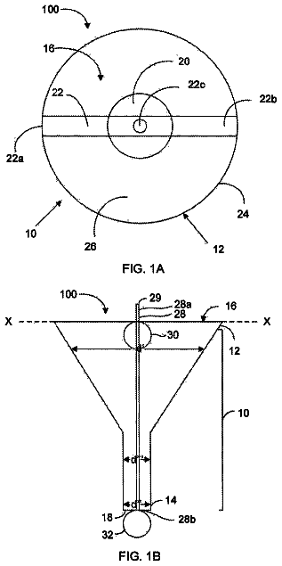
Sheet 1 of 9 from the published document. All sheets in the USPTO PDF
A device for determining the fill level of a medium in a container having at least one electronic device and at least one signal conductor arrangement. The electronic device supplies the signal conductor arrangement 5 with electromagnetic signals. To provide a device for determining the fill level, the signal conductor arrangement has several emitting devices and the electronic device provides at least one measure for an emitting behavior of at least one emitting device.
Field of the Invention The invention relates to a device for determining the fill level of a medium in a container. The device has at least one electronic device and at least one signal conductor arrangement. The electronic device supplies the signal conductor arrangement with electromagnetic signals. Description of Related Art The medium is, for example, bulk goods or a liquid and the container is, for example, a tank, a silo or a channel. The signals are, in particular, high frequency or microwave signals. It is known in industrial process automation either to continually measure the fill level of the medium or to specifically monitor particular limit levels. Such devices for monitoring limit levels are also called fill level or limit level switches. They are used, for example, depending on the mounting position, for overflow protection, idle state protection or pump protection. If the
1 of 9 drawing sheets so far from the published document, cropped to the drawing. Every sheet is in the USPTO PDF.
What the patent claimed, word for word. All of it is now free to use.
Field of the Invention
The invention relates to a device for determining the fill level of a medium in a container. The device has at least one electronic device and at least one signal conductor arrangement. The electronic device supplies the signal conductor arrangement with electromagnetic signals.
Description of Related Art
The medium is, for example, bulk goods or a liquid and the container is, for example, a tank, a silo or a channel. The signals are, in particular, high frequency or microwave signals.
It is known in industrial process automation either to continually measure the fill level of the medium or to specifically monitor particular limit levels.
Such devices for monitoring limit levels are also called fill level or limit level switches. They are used, for example, depending on the mounting position, for overflow protection, idle state protection or pump protection.
If the medium reaches a predetermined fill level or falls below such, the switches generally generate a signal that, e.g., interrupts a fill process or triggers a safety mechanism or causes the closing of a drain valve.
It is known, for example, to detect limit levels capacitively e.g., German Patent Application DE 100 23 850 A1, using conductivity measurement e.g., International Patent Application Publication WO 97/37198 A1 and corresponding U.S. Pat. No. 5,861,811 or using mechanically swingable sensors e.g., German Patent Application DE 198 25 501 A1.
Furthermore, a device is known from International Patent Application Publication WO 2013/167384 A1 and corresponding U.S. Patent Application Publication Patent 2015/082881 for detecting a limit level of a medium, in which the frequency of an output signal of a resonator is evaluated. The resonator is in contact with the interior of the chamber that contains or conducts the medium. Detection thereby occurs in that the frequency of the resonator is exploited depending on the dielectric constant of the medium. In one design, the resonator is designed as a micro strip line or as an emitting device.
It is known from a completely different field of application to determine the moisture of objects in a container using reflector switches, see German Patent Application DE 10 2004 016 725 A1.
A strip line antenna for fill level recognition is, for example, provided in German Patent Application DE 199 35 743 A1. Thereby, in one design, two receivers for microwave signals are used for the redundant monitoring of the fill level.
An exemplary design of emitting devices that are used in the field of fill level measurement is disclosed in German Patent Application DE 10 2006 019 688 B4 and corresponding U.S. Pat. No. 7,710,328. Such emitting devices consist in general of metal surfaces that are present on or in printed circuit boards or other substrates.
It is additionally known in the prior art to further add metal surfaces acting as reflectors.
So-called patch antennae are also known in the prior art other terms are “flat antenna” or “micro strip antenna”. An array is created by interconnecting several antennae. It is thereby known to create different resonance structures: half-wave or quarter-wave, see e.g., DE 699 36 903 T2 and corresponding U.S. Pat. No. 6,218,990. Panel antennae can be used for measuring the surface structure of media, see e.g., European Patent Application EP 1 701 142 A2 and corresponding U.S. Pat. No. 7,408,501.
Panel antennae that are arranged in ceramic structures are used for fill level recognition, for example according to International Patent Application Publication WO 2009/121530 A1 and corresponding U.S. Pat. No. 8,474,314.
In the fill level switch according to European Patent Application EP 1 956 349 A2 and corresponding U.S. Pat. No. 7,730,780, electromagnetic signals are coupled into each of a measuring conductor arrangement and a resonance conductor arrangement, wherein the signal of the measuring conductor arrangement can interact with the medium, whose fill level is to be monitored.
A device having microwave sensors for the specific use of monitoring the fill level of a blood reservoir is described in German Patent Application DE 195 16 789 B4. These sensors are attached outside of the reservoir and radiate through its wall. It is described, in one design, that several sensors are attached at the same level. It is further provided that sensors are attached at different levels in order to already be able to signal that the fill level is approaching a critical limit level.
Contaminants or the deposition of medium on the container wall or especially on the sensors are problematic for the above-mentioned devices or, respectively, limit level switches. This can lead to false signals or can even prevent the detection of the reaching or falling below a fill level.
Originating from these problems, it is known, for example, in membrane oscillators to shake off gas bubbles during a cleansing phase see German Patent Application DE 10 2008 050 445 A1.
In safety-critical uses, it is further known to design the sensors or devices redundantly. In the simplest case, two measuring devices are used that have the same function.
In particular, the following types of redundancy are thereby differentiated:
In hot spare, several sensors are actively operated. A so-called voter evaluates the individual results, wherein, if necessary, the majority decides.
In cold redundancy, several sensors are present, however, only one sensor is active. Based on the evaluation of the signals of this individual sensor, further sensors are activated, if need be.
In standby or passive redundancy, again, several sensors are present and, again, only one sensor is active. The non-active sensors are thereby in a standby state. In the case of an error of the active sensor, another sensor is switched on.
Thereby, the redundancy can be homogeneous or diverse. This means, for example, that either the same type of sensor or the same components are multiply used, or that the individual sensors or components come from different producers or are based on different principles.
The object of the invention is to provide a device for determining the fill level that is advantageous compared to the prior art.
The device according to the invention in which the above derived and described object is achieved is initially and essentially wherein the signal conductor arrangement has several emitting devices and that the electronic device provides at least one measure for an emitting behavior of at least one emitting device.
The electromagnetic signals are, in particular, microwave signals. Thus, in one design, the device according to the invention can, in particular, be called a high frequency HF fill level switch.
The emitting devices, of which at least two are present and which also can be called individual elements of the HF fill level switch, are to be understood as impedance converters in one design.
Thereby, the wave impedance of a line, via which the electromagnetic signal is supplied to the emitting devices, is adapted to the wave impedance of the area in front of the emitting devices. This area is, in particular, a free space in the case that the device is used as overflow protection.
In that the impedance matching is monitored, it can be assumed that when a change in the matching occurs, a change in the space in front of the emitting device has occurred. In the case of the use as a limit level switch, this is a change in the degree of coverage.
The emitting devices are, in one design, designed as antennae and, in a further design, in particular, are designed as patch antennae.
Preferably, the emitting devices or patch antennae are designed to be flat.
The emitting devices preferably have a relatively narrowband impedance matching.
In patch antennae as an exemplary design for emitting devices, such a narrowband impedance matching can be ascribed to the half-wavelength resonance being implemented via a patch antenna. Thereby, only the frequency whose half-wavelength is as large as the geometric length of the patch antenna experiences impedance matching.
In one design, the emitting devices are designed in such a manner that the direction of emission is orthogonal to both directions of expansion of the emitting device designed as antenna.
The materials surrounding the respective emitting device or the respective patch antenna are important for impedance matching, since the materials shorten the wavelength of the signal, for which impedance matching occurs, by the root of the effective permittivity.
The permittivity, commonly denominated with the Greek lowercase epsilon c, is also called dielectric conductivity or dielectric function and describes the permeability of a material for electrical fields.
The link between material permittivity and impedance matching characteristic is used in the device according to the invention in order to identify the fill level of the medium in a container.
If the material e.g., due to an exchange of air to the medium to actually be detected, and thus also the permittivity, in front of an emitting device or, in particular, in front of a patch antenna changes, then the effective permittivity around the antenna/emitting device changes as does the frequency that represents an impedance matching for the emitting device.
Thus, on the other hand, if a change in the impedance matching is recognized by the device according to the invention, then this can be ascribed to a change in the fill level.
Additionally or alternatively, a change in the material characteristics is concluded.
The above correlations can also be described in other words as follows for the exemplary use as overflow protection:
If an emitting device is supplied with an electromagnetic signal, whose frequency is the same as the resonance frequency that is set by the emitting device not covered by medium, i.e., free, and if the emitting device is not covered by medium during supply with the signal, then the signal is emitted in the interior of the container, which is, e.g., a tank.
Since, in this case, no or very little reflection occurs on the emitting device designed as antenna, the energy of the wave returning from the emitting device is extremely small.
If the fill level of the medium in the container changes so that the emitting device is reached, then the resonance frequency of the emitting device is also shifted. However, the supplied electromagnetic signal thereby experiences a stronger reflection, which in turn results in a greater energy of the returning wave.
Depending on the magnitude of change of permittivity that results from that transition between a free emitting device and one covered with medium, the emitting device emits at a different, neighboring frequency small permittivity change or there is no longer any emission large permittivity change.
The described effect can be understood as a near field effect of the antenna or, respectively, the emitting device.
The measure for emitting behavior of at least one emitting device determined by the electronic device consists, in one design, of identifying that the resonance frequency of the at least one emitting device has changed. Based on this change, it can then be concluded that the degree of coverage of the emitting device by the medium in the container has changed or that a change in the medium itself exists.
Due to the plurality of individually operable emitting devices, several individual results are available that can be combined for determining the fill level.
The measuring results of the—in particular, of all—emitting devices are, thus, in one design, processed into one overall result using a suitable processing unit e.g., a measuring device or, in general, an electronics unit, which is implemented by a microprocessor. In another design, the individual results are consolidated using logical units.
The following designs relate to advantageous designs of the device that are used, in part, for implementing the above-described correlations.
It is provided in one design that the electronic device evaluates at least one impedance behavior of the at least one emitting device as a measure for the emitting behavior of at least one emitting device.
In this design, the electronic device preferably monitors the impedance matching of at least one emitting device.
If the impedance matching changes, this is, in one design, ascribed to a change arising in front of the emitting device, i.e., in particular within the container and thus on the emitting side of the emitting device. This change is thereby interpreted, in particular, as a change in fill level and is signalized as such.
In an associated design, the electronic device determines an impedance value and/or a change of impedance of at least one emitting device.
In one design, the electronic device determines an absolute value for the impedance and, additionally or alternatively, determines whether the impedance has changed.
In one design, at least one input reflection of the at least one emitting device is determined by the electronic device for the measure of the emitting behavior. In this design, the electronic device evaluates the input reflections of at least one emitting device that yields signals as a result of the supply with electromagnetic signals. The reflection is thus, in this design, a measure for adapting the electromagnetic signals to the present resonance conditions.
In one design, the electronic device supplies at least one emitting device with electromagnetic signals of a predeterminable frequency.
The frequency, in one design, depends on whether the device according to the invention is used as overflow protection or as idle state protection, i.e., whether a change from uncovered to covered state or from covered to uncovered state is to be detected.
In a further design, the frequency depends on the material characteristics such as e.g., permittivity of the material surrounding the emitting device. This, thus, also relates to the nature of the support element or to a possibly existing protection layer.
If all emitting devices are located in or on one support element, then this simplifies the assembly in the process area due to the reduction to one mechanical component.
In one design, several emitting devices are supplied with the same electromagnetic signal.
In one design, the predeterminable frequency of the electromagnetic signals corresponds essentially to the resonance frequency of the emitting device not covered by medium. In this design, it is detected when the medium reaches the relevant emitting device, i.e., overflow protection takes place.
In an alternative design, i.e., in particular when used as pump protection or idle state protection, the predeterminable frequency essentially corresponds to the resonance frequency of the emitting device covered by the medium.
If the medium in front of the emitting device changes or if the emitting device is no longer covered by medium, then the frequency of the signals supplied to the emitting device no longer corresponds to the current resonance frequency. This can be accordingly detected by the electronic device and identified or signalized.
In an additional or alternative design, the electronic device varies the frequency of the electromagnetic signals that are supplied to an emitting device or several emitting devices within a predeterminable frequency band. In this design, a frequency sweep is carried out and the frequency behavior of the emitting device or emitting devices is measured thereby. This allows for a very exact determination of the current resonance frequency, for example in a plurality of measuring surroundings or process conditions, which in turn can be informative about the surroundings and thus also about the measuring medium.
It is provided in one design that the electronic device has at least one reflector switch for the actual determination of the fill level by the individual emitting devices, i.e., whether the fill level has been reached or not.
Thereby, the reflector switch is assigned to one emitting device.
Furthermore, the reflector switch is designed in such a manner that is provides a measure for an emitting behavior of an emitting device.
The reflector switch detects whether the emitting device is covered by the medium or whether, e.g., gas or common ambient air is located in front of the emitting device.
The measure for the emitting behavior, in one design, is found in the information of whether or not the medium covers the emitting device.
The following exemplary designs are given for the reflector switches or, in general, the metrological design of the electronic device.
The respective emitting device is continuously supplied with a mono-frequency signal in an absolute value CW continuous wave detection. The frequency is chosen in one design so that it corresponds to the resonance frequency of the emitting device in the case that the medium does not come into contact with the antenna. Thus, if the antenna is free, it emits the electromagnetic signal.
The reflector switch thus permanently monitors the adapting of the antenna at the set supply frequency.
In one design, the reflector switch issues a DC voltage that is dependent on the relation between the power supplied to the antenna and the reflected power.
A comparator that is downstream from the reflector switch in the electronic device compares, in one design, the generated DC voltage from the reflector switch with an external predetermined reference voltage and generates an evaluation.
If there is no medium or ambient air in front of the antenna—when used as overflow protection, i.e., detecting when the fill level has been reached—then the antenna is adapted and its input reflection is small. Thus, the reflector switch generates a voltage that is below the reference voltage so that the comparator issues a low level.
If the medium is located in front of the antenna—in the above-mentioned use—the resonance frequency is shifted and the antenna has a worse adapting behavior for the applied frequency of the signal. Thus, the input reflection of the antenna is increased and, thus, also the DC voltage generated by the reflector switch. If the DC voltage is greater than the reference voltage, the comparator issues a high level that signalizes that the limit level has been reached.
In the case that the respective emitting device is covered by a protective layer, or in the case that the medium to be detected has a very low permittivity, in one design, it is provided that the above-described absolute value CW detection is broadened to a complex detection.
Thereby, as an addition to the above design, both the signal supplied to the emitting device as well as the reflection signal tapped by the antenna are separated. In addition to the above-described simple reflector switch, both signals are also supplied to a second measuring or evaluating site. A 90° phase shifter is thereby provided in one of the two signal paths.
The above-mentioned reflector switch supplies the “in-phase” signal and the second measuring site supplies the “quadrature” signal.
Both signals are preferably digitized, in one design, for example, in order to be further processed in a microprocessor. Hereby, a phase evaluation of the reflected signal is then possible. This has the advantage that the phase shift due to the reflection of the signal on the medium is a very sensitive measure.
In the case, in which the medium causes large losses of the signal of the emitting devices, the adaptation curve of the antenna broadens over the frequency.
In order to still reliably detect the reaching of a limit level, it is thus provided that, in one design, a broadband adaptation curve of the emitting devices is determined, i.e., measured.
Thus, in one design, the emitting devices are supplied with signals that lie within a predeterminable frequency range.
The DC voltage of the respective reflector switch is directly digitized in one design. This allows for the respective value of the reflection to be assigned to the frequency of the signal that is supplied to the respective emitting device.
After a complete frequency sweep, the obtained adaptation curve is evaluated, wherein the lowest determined DC voltage of the reflector switch is assigned to the resonance frequency of the emitting device.
In one design, the broadband detection is combined with the above described complex variation and the phase evaluation possible therewith.
In one design, the signal that is supplied to the assigned emitting device is supplied to the reflector switch.
In one design, the reflector switch monitors the adaptation of at least one emitting device during supply with the electromagnetic signal.
In one design, the reflector switch is assigned only to one, single emitting device, in that the reflector switch is assigned to exactly one emitting device and provides a measure for the emitting behavior of only the one emitting device.
In a further design, each emitting device is assigned one reflector switch. Thus, in this design, the number of emitting devices is the same as the number of reflector switches.
In another design, the at least one reflector switch is assigned to several emitting devices and provides at least one measure for the emitting behavior of the emitting devices assigned to it.
The individual reflector switches each generate information about whether—depending on the type of use—the medium has reached or fallen below the fill level assigned to the emitting device. The individual results of the reflector switch are then processed or, respectively, completely evaluated in the electronic device.
In one design, the electronic device is designed such that, after an emitting device is supplied with at least one electromagnetic signal, the electronic device taps and evaluates at least one reflection signal from the emitting device.
In the following designs, the pure determination or, respectively, monitoring of the fill level is expanded to further measuring variables.
Thus, in one design, the electronic device determines, in addition to the fill level, at least one further piece of information about the medium based on the emitting behavior of the emitting device.
This further information, in one design, is information about a separating layer between two different phases or substances in the medium of the container.
In an additional or alternative design, the electronic device detects information about a permittivity of the medium.
For example, based on a precise evaluation of at least the reflected signal, information is obtained about the medium that is located in front of the emitting device. The permittivity is thereby used in order to differentiate between different media or in order to determine a change in the medium.
In one design, the presence of different materials is identified based on the permittivity.
In order to identify the medium using the permittivity, in one design, broadband measurement is carried out, in which the electromagnetic signals are run through a frequency band to determine the resonance frequency and, thus, the medium.
The medium that was used for carrying out a calibration of the device according to the invention is also relevant for determining of the additional information.
In one design, the calibration medium is air.
In an alternative design, the medium that is to be monitored and measured is also the calibration medium.
In one design, the phase shift of the complex phasor is evaluated in order to also identify small changes or differences of the permittivities.
In one design, contamination of at least one emitting device due to accumulation of the medium and gradually changing resonance conditions caused thereby is identified.
Overall, a change of resonance behavior of at least one emitting device is determined or identified by the device according to the invention via the electronic device.
Different individual measured values can be generated and unified into an overall picture due to the number of emitting devices that are essentially designed in the same manner. Thus, several individual sensors are combined into one multi-sensor.
In one design, each emitting device is individually evaluated.
The following designs ensue:
In one variation, each emitting device is connected to its own signal feed and its own reflector switch.
In an alternative design, the emitting devices are supplied by a signal source, however, they each have their own reflector switch.
In an additional design, the emitting devices are supplied by a common broadband signal generator. Thereby, however, the lengths of the lines between the signal generator and the individual emitting devices differ from one another such that the reflections occur at times clearly different from one another and allow for assignment to the emitting devices.
In one design, at least a part of the emitting devices are evaluated together.
It is provided in one design that a support element at least partially supports the signal conductor arrangement. At least part of the emitting devices is attached on or in the support element.
In a further design, all emitting devices are located on or in the support element so that the emitting devices can also be mounted at their operation site via the support element.
The majority of emitting devices on one support element can lead to a coupling of the individual emitting devices. This can result in crosstalk of high frequency signals from neighboring emitting devices.
Thus, for example, de-coupling is required using one of the following methods: space-, time-, frequency-, code- and/or polarization division multiplexing.
The device according to the invention is, in particular, a so-called limit level switch that shows whether or not the medium has reached or fallen below a fill level—i.e., a limit level.
The device according to the invention detects the fill level of the medium in that a signal conductor arrangement is supplied with electromagnetic signals and in that it is identified whether the medium covers the signal conductor arrangement.
Thereby, the signal conductor arrangement has several emitting devices, which are each supplied with the electromagnetic signals.
Redundancy, for example, can be created by the plurality of emitting devices. Furthermore, several level limits can be identified. It is additionally possible to verify measurement values.
The signal conductor arrangement, i.e., the emitting devices, is thereby attached in or on a support element. The support element serves as a substrate for supporting a mechanical structure or for easier mounting of the plurality of emitting devices.
The emitting devices are located, at least in part, in particular, on the side of the support element facing the medium—in the mounted state or are at least attached into or on the support element so that an interaction with the medium can take place.
In one design, the emitting devices are separately created components that are introduced to or deposited on the support element after their production.
In a further design, the emitting devices are first created in or on the support element.
The support element is thereby designed, in particular, so that it can be inserted into a wall of the container. The support element can thus be inserted, in particular, into a corresponding recess in the wall, for which the dimensions need to be compatible.
Since the device is, preferably, a limit level switch, the support element can preferably be inserted into a side wall of the container.
In one design, the support element can be screwed into the wall. In this design, the overall result is a fill level or limit level switch designed as a screw-in sensor.
Due to the—at least two—emitting devices, it is detected whether the medium is located close to the respective emitting device or, respectively, covers it. Therefore, depending on the use, the reaching or falling below a fill level assigned to the respective emitting device can be detected.
Depending on the location at which the individual emitting device is located in the mounted state in the container wall, i.e., depending on the installation site, one fill level is monitored by each of the emitting devices.
The fill levels thereby can be different, can be essentially the same, can overlap—depending on the desired measuring accuracy—, or can be adjacent to one another.
Thus, in one design, fill level ranges are defined that are commonly monitored by several emitting devices.
Which fill levels are assigned to the individual emitting devices, on the hand, is determined by the dimensioning and arranging of the emitting devices on the support element as well as by the achievable local resolution of the measurements and, on the other hand, is determined by the end position of the emitting device after assembly.
On that basis, it is provided in one design that the processing of the individual results or individual measurements or, respectively, individual fill level monitoring of the individual emitting devices is adapted to the specific use or, respectively, to the orientation resulting after assembly in relation to the container and is not previously specified.
Due to the plurality of emitting devices, redundancy can, on the one hand, be created in that at least two emitting devices monitor the same fill level or fill level range.
For this, in one design, at least two emitting devices are attached relative to a longitudinal axis of the support element at the same level. In the mounted state in the container, the longitudinal axis can thereby deviate from a longitudinal axis of the container.
Redundancy is configured in this design when the emitting devices in the attached state are located at the same level in the container.
If they are located at different levels of the container, then they are assigned a different fill level, at or below the level that they monitor.
In an additional or alternative design, at least two emitting devices are attached at different levels in relation to a longitudinal axis of the support element. The arrangement of the emitting devices thereby relates to the production of the device and not necessarily to the mounted state in the container.
If the emitting devices are located at different levels, different fill levels can be identified by them, or it is possible to identify the approaching of the medium to a certain level limit. It is thereby also validated whether the limit level has been reached, since—in the case of the use as overflow protection—a lower-lying fill level of the medium has to be reached.
Depending on the mounting position, however, the emitting devices can be assigned the same fill level or a fill level range. In each case, this depends on how the support element is inserted in the wall of the container or what the end position of the support element is.
Dynamic measurements or plausibility checks of the individual measuring signals allow for the detection of different fill levels. Accordingly, the reliability of fill level determination can thereby be respectively increased.
A plurality of individual sensors that are—at least in part—operated individually, and thus, can supply individual measured values or, in particular, switching signals thereby result in the device for fill level determination due to the individual emitting devices.
Thus, the invention also relates to a measuring arrangement having a container and a device for determining the fill level attached to a wall of the container. Thereby, the device described here can also, in particular, be called limit level switch in this context.
The materials of the support element are adapted thereby to the use or to the respective medium.
In one design, the emitting devices are supplied with the same signals, and in a further design, they are supplied with different signals.
In one design, at least one of the emitting devices is an antenna. The antenna is, for example, a miniaturized horn antenna.
In a further design, at least one of the emitting devices is a patch antenna. The patch antenna is comprised of a corresponding conductor structure, as it is known from the prior art.
In particular, in one design, all emitting device are designed essentially identically. Thus, in this design, the emitting devices are either antennae or, in particular, patch antennae.
The conductor structures or antennae thereby consist, at least in part, of a metal such as, e.g., copper, silver, gold, or nickel.
In that the emitting devices are arranged on a common support element or substrate, or generally close to one another, there is a risk that the antennae couple with one another.
The following examples are possible variations for de-coupling:
In one variation, metal surfaces particular designs are also called “via fences” or “picket fences” are arranged between the individual emitting devices. In such a separation, a completely parallel operation of all emitting devices is possible.
Further separation is implemented in one design in that different running lengths are created for the signals between a signal source and the individual emitting devices. Thereby, a signal coming from the signal source reaches the emitting devices at different points in time.
A parallel operation of all emitting devices is only conditionally possible in the case of such a temporal separation. Due to the rapid—compared to typical change of the fill level—method of detection, the measurements via the individual emitting devices occur quasi simultaneously.
A separation in the frequency range is further or additionally provided in that the emitting devices are supplied with signals having different frequencies.
Additionally or alternatively, the emitting devices differ from one another in view of their resonance frequency due to their geometry or materials, so that this already denotes a de-coupling.
In one design, a further separation is achieved by code multiplexing. Thereby, the signals of the signal source are encoded, wherein each emitting device is assigned one code sequence.
Thus, in one design, a filter is located in front of the emitting devices, which allows the signals to pass to the respective emitting device according to their code sequence. The same occurs in front of the reflector switches, so that only the respective suitable returning signals are evaluated.
In one design, at least a portion of the emitting devices differs from another portion at least in view of the spatial polarization of the respectively emitting electromagnetic signals. The individual emitting devices, thus, each have different preferred polarization and emit signals having different spatial polarization.
In one design, emitting devices have polarization that is at right angles to the adjacent device.
In one design, further structures are provided for de-coupling, so that a portion of the emitting devices, in particular also in conjunction with a spatial gap, emits signals with the same polarization.
It is provided in one design that at least a portion of the emitting devices is arranged essentially rotationally symmetrical in relation to the support element.
In one design, the support element is separated into several angle sections on one side, in each of which at least one emitting device is located.
The angle sections, in particular, have the same size in one design.
If, in this design, a subcategory of n emitting devices from a total of m emitting devices is distributed evenly over a support element—that is circularly designed, at least in this area that supports the emitting device—then each of the n emitting devices is assigned an angle section of 360°/n.
At least one further emitting device, in one design, is located in the middle of the support element or in the middle of the rotationally symmetrical arrangement of emitting devices, which thus also represents the center of the arrangement of—preferably rotationally symmetrically arranged—emitting devices.
In an alternative design, the middle is free of emitting devices.
In an additional design, more than one emitting device is arranged centrally on the support element.
The rotational symmetry is, in particular, advantageous with the design of the support element in that the support element is screwed into the wall of the container. Thus, any free rotation is possible and a predetermined end position does not necessarily have to be achieved.
In one design, the support element is essentially disk-shaped. This form makes the insertion into the wall of the container easier.
Thereby, the form of the wall or a recess in the wall and the outer geometry of the support element are attuned to one another such that screwing in—preferably with a sealing function—is possible.
In order to attach the support element in the container, it is provided in one design that the support element has an outer surface designed as an outer threading. The type of threading is, thereby, to be matched to an inner threading of a recess in the container wall or possibly to an adapter to be correspondingly provided.
In an alternative or additional design, the support element can be sealingly inserted into the wall of the container.
In one design, the support element can be screwed so tightly into the wall, that a sealing function results.
In a further variation, at least one sealing lip is provided and in an additional variation, recesses are provided for sealing elements, e.g., O-rings or for the insertion of a sealing material.
In a further design, an adapter is provided, which, in particular, allows an alignment of the support element or the emitting devices in relation to the container.
The support element is formed, at least in part, of a multi-layer ceramic, wherein at least a portion of the emitting devices is arranged between the individual layers of the multi-layer ceramic. The emitting devices are thus protected from the medium by the support element. However, the support element is thereby designed in such a manner that an interaction between the emitting device and the medium is still possible.
In one design, the support element is formed at least in part of a ceramic and/or of a plastic and/or of glass.
Additionally or alternatively, the support element is formed, at least in part, of a circuit board material or of a HF substrate.
In one design, the support element is produced essentially entirely of one of the above-mentioned materials.
In one design, wherein the support element is of ceramic, the emitting devices and also the supply and outlet lines are generated, e.g., using a thin or thick layer method.
In a further design, the support element is designed to be flat, at least on the side facing the medium.
In an alternative design, the support element has a convex or concave course on the side facing the medium.
The outer contour of the support element contributes to the medium or possibly occurring condensate flowing or dripping from the support element.
In one design, the device allows for use in an area at risk for explosion. For this, in particular, the components and especially the emitting devices are accordingly dimensioned and designed.
Thus, in one design, it is particularly provided that a electrically nonconductive surface facing the medium or the process has a maximum size of 4 square centimeters.
Alternatively, the electrically nonconductive part of the surface of the support element facing the medium is surrounded by a metallic, grounded structure, wherein the projection surface of this framed surface is less than 16 square centimeters.
In order to protect the emitting device from the medium or from the process conditions prevailing in the container, at least one protective layer is provided in one design.
The protective layer is thereby applied in the direction of the medium or process or container interior in front of an emitting device or in front of the entirety of the emitting devices.
In one design, the protective layer is dielectric.
In one design, the protective layer is a coating.
The description continues in the full USPTO document.
About 6,455 words. The USPTO PDF has it with every drawing.
Fees are due 3.5, 7.5 and 11.5 years after grant. This patent expired on December 26, 2025, so the fee marked "not paid" was the one that went unpaid.
DEVICE FOR DETERMINING THE FILL LEVEL OF A MEDIUM
Filed Dec 2015 · published Jul 2016Device for determining the fill level of a medium
Filed Dec 2015 · granted Dec 2017Earlier publications, parents and continuations. None of them can still be enforced, or this patent would not be listed.
Prior art cited by the examiner or applicant. Useful when you check your own idea for novelty.
Everything on this page comes from the documents linked above.