 Lapsed, fee not paid6 drawings
Hardware & Electronics · US 9,847,674 B2
Smart connector housing
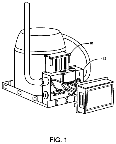
A connector includes a main housing element for holding smart connector circuitry.
US 9,847,736 B2 · Assignee: SoftKinetic Sensors NV · Inventors: Grootjans; Riemer et al.
Sheet 1 of 6 from the published document. All sheets in the USPTO PDF
An electronic driver circuit for LEDs and LASERs is provided for use in time-of-flight applications featuring a high efficiency of energy-conversion and a high precision of distance-measurements based on a dual conversion circuit. A voltage to voltage DC-DC conversion is hereby merged with a DC-voltage to pulsed-current booster, this booster operating at a time-of-flight modulation frequency. At the start of a new measurement cycle, the PWM signal for driving the DC-DC conversion is updated in response to currents observed during previous illumination periods.
Optimal powering of light sources such as LEDs for time-of-flight (TOF) devices requires specialized regulators that minimize intensity variations, e.g. with battery voltage and uniform pulse output. For this purpose, there are two regulators types often used: inductor-based boost converters and capacitor-based charge-pump converters. Each regulator type has specific advantages/disadvantages. Application note 3243 (http://www.maxim-ic.com/an3243) of Maxim Integrated Products describes a comparison between LED Boost Converters and Charge Pump circuits. This article compares state-of-the-art regulators, namely the MAX1561 boost converter versus the MAX1573 charge pump. FIG. 7 shows the boost converter and the charge pump of FIG. 1 of this document. The article suggests advantages for the charge pump. A time of flight camera usually comprises an illumination device configured for illuminati
1 of 6 drawing sheets so far from the published document, cropped to the drawing. Every sheet is in the USPTO PDF.
What the patent claimed, word for word. All of it is now free to use.
This application is a §371 national stage entry of International Application No. PCT/EP2012/063697, filed Jul. 12, 2012, which claims priority to British Patent Application No. GB 1112115.9 filed Jul. 14, 2011, the entire contents of which are incorporated herein by reference.
The present invention relates to an electronic driver circuit for a load especially for light sources of which light emitting diodes (LED) or OLED's or lasers or laser diodes are examples. In particular, the present invention relates to a driver circuit for an illumination device for a range finding device, a time of flight camera, or a time of flight sensor as well as to an illumination device for such device or camera as well as to the device or camera itself.
Optimal powering of light sources such as LEDs for time-of-flight (TOF) devices requires specialized regulators that minimize intensity variations, e.g. with battery voltage and uniform pulse output. For this purpose, there are two regulators types often used: inductor-based boost converters and capacitor-based charge-pump converters. Each regulator type has specific advantages/disadvantages.
Application note 3243 (http://www.maxim-ic.com/an3243) of Maxim Integrated Products describes a comparison between LED Boost Converters and Charge Pump circuits. This article compares state-of-the-art regulators, namely the MAX1561 boost converter versus the MAX1573 charge pump. FIG. 7 shows the boost converter and the charge pump of FIG. 1 of this document. The article suggests advantages for the charge pump.
A time of flight camera usually comprises an illumination device configured for illuminating an object, and a detection device configured for detecting light received from the illuminated object. The time of flight camera is configured for determining a phase difference between the light emitted by the illumination device and light reflected by the object and received by the detection device, in order to reconstruct an image of the illuminated object.
US 2011/0018451 A1 describes an light emitting diode (LED) driver circuit configured for driving a plurality of LED strings which are arranged in parallel to one another and each of the LED strings comprising a plurality of LEDs connected in series to one another. The LED driver circuit comprises a voltage regulation loop and a current regulation loop for controlling an amount of light emitted by the plurality of LEDs. The voltage regulation loop and the current regulation loop are configured for controlling an amount of voltage inputted to the LED driver circuit with respect to a measured output voltage and a measured current of the LED strings, respectively.
It is an object of the present invention to provide an electronic driver circuit for a load especially for light sources of which light emitting diodes (LED's) or OLED's or lasers or laser diodes are examples. In particular, it is an object of the present invention to provide a driver circuit suitable for an illumination device for a range finding device, a time of flight camera, or a time of flight sensor as well as an illumination device for such device or camera as well as the device or camera itself.
It is an advantage of embodiments of the present invention to provide an electronic driver circuit for light sources such as LEDs, OLED's, LASERs and LASER diodes, for use in time-of-flight applications featuring a high efficiency of energy-conversion and a high precision of distance-measurements based on a dual conversion circuit.
In one aspect he present invention provides a boost converter circuit for use with a load and a DC power supply for conversion of DC power to a pulsed wave for driving the load, comprising: a DC-DC converter circuit comprising a terminal for receiving a DC voltage from the DC power supply, a first inductance, a charge storage device such as a capacitance and first and second switching means, the first inductance being coupled to the terminal; the first switching means being adapted to charge the charge storage device such as a capacitance from the inductance at a first frequency, and a DC voltage-AC current converter circuit comprising a second inductance coupled to the charge storage device such as the capacitance and third switching means for driving the inductance as a pulsed wave current source for the load at a second frequency, the second frequency being higher than the first frequency.
The second switching means can be diode means such as a diode or a diode circuit or it can be a switch which is adapted to switch from open circuit to conducting in the same situations as a diode. Diodes can also be incorporated in other electronic components. The capacitance can be a capacitor or a capacitor circuit or any other device with a suitable capacitance. The first and/or second inductances can be an inductor or an inductor circuit or any other device with a suitable inductance.
Preferably, fourth switch means are provided for interrupting current in the load. This has the advantage that light sources do not emit any light during dark periods, thus saving power.
Preferably, current sensing means for sensing the current in the load are provided. This can be a resistor in series with the load, for example.
Preferably, a feedback loop is provided for controlling the boost converter circuit in response to the output of the current sensing means. A negative feedback loop helps to maintain stability of operation.
Preferably, the feedback loop and the DC-DC converter circuit control the current in the load in response to the output of the current sensing means. An advantage is that the intensity of illumination can be controlled.
In a preferred embodiment the control of the current is by PWM control of the DC-DC converter circuit. PWM control allows precise and rapid control of the total amount of charge that is fed to the capacitor from the first inductor. This controls the amount of current that can be extracted from the capacitor by the second inductance.
Especially for applications where the current through the load must be kept constant over a certain time, the feedback loop can be adapted to control or modify the operation of the DC-DC converter circuit only at time intervals and hence not disturbing operations at other times.
The boost circuit is particularly well adapted to drive a load that is one or more light sources. This allows the circuit to be used with a display backlight, in TOF sensors or cameras, range finders, in optoelectronic transducers and converters, e.g. for use with optical fiber networks and other optical devices. The one or more light sources can be one or more light emitting diodes or lasers or laser diodes. The light sources can be supplied separately and are not necessarily part of the boost converter circuit.
Preferably the DC voltage-AC current converter circuit is adapted to only draw a DC current from the DC-DC converter circuit. This reduces EMI.
Preferably an output is provided for a PWM duty cycle value. This can be used to check if the duty cycle is within allowable limits.
Optionally the PWM control can have a start mode and a stop mode. This offers the advantage of ramping up current to the load at start and ramping down at stop thus allowing a graceful power up and down.
In a further aspect of the present invention a range finding device, camera or sensor can be adapted to determine a distance to an object by measuring light emitted by the one or more light sources and reflected by the object within measurement cycles, whereby the boost converter circuit is adapted to update the PWM control before a measurement cycle. This has the advantage that the update is not done during a measurement cycle which could render erroneous distance measurements.
Hence, according to an exemplary aspect of the invention, a driver circuit for an illumination device for a time of flight camera is provided. The driver circuit is connectable to an illumination unit configured for emitting light. The driver circuit comprises the DC-DC converter, a DC voltage-AC current converter circuit, an illumination unit, and a control unit configured for controlling the DC-DC converter in response to a signal indicative of an amount of the light emitted by the illumination unit. The DC-DC converter is connectable to a power supply and configured for supplying power to the DC voltage-AC current converter circuit in the form of a pulse generator connected in series to the DC-DC converter and configured for converting the output of the DC-DC converter to a pulse train,
Accordingly, the driver circuit comprise a feedback loop or mechanism, in order to adjust the amount of light emitted by the illumination unit based on an actual amount of the emitted light in that the control unit is configured for controlling the DC-DC converter in response to (and particularly based on) a control signal indicative of the amount of light emitted by the illumination unit.
The operation of the feedback loop may be restricted to certain time intervals which are preferably synchronized to the timing of the measuring cycles.
The DC-DC converter may be configured as a buck regulator, a voltage step up or boost converter or a buck-voltage step up regulator. Here, a buck regulator may be configured for down-converting a voltage inputted to the buck regulator. A voltage step up converter may be configured for increasing a value of an inputted voltage to the voltage converter. A buck-voltage step up regulator may be configured for down-converting and/or up-converting an inputted voltage value. Thus, the driver circuit may employ a commercially available electronic component for the voltage adaption such that the driver circuit may comprise low manufacturing costs.
The pulse generator may comprise an energy storage element such as an inductor, a switch and a ground plane, wherein the energy storage element, the switch, and the ground may be connected in series to one another, and wherein the switch may be connected in parallel to the illumination unit. The switching of the switch may allow to connect the energy storage element with ground via the switch or via the illumination unit. During a time in which the energy storage element may be connected to ground via the switch, a charging of the energy storage element may be accomplished. Further, during a time in which the energy storage element may be connected to ground via the illumination unit, a discharging of the energy storage element and thus an emission of light by the illumination unit may be accomplished. Accordingly, the energy storage element may be pre-loaded prior to the emission of the light by the illumination unit, whereby the illumination unit may be supplied with energy at once, and a rise time of the light emitted by the illumination unit may be significantly shortened. Thus, a fast start and/or end of an emission of the light by the illumination unit may be accomplished, and a waveform of the emitted light may comprise a sharp rising and/or falling edge. The latter may be particularly favorable in connection with a time of flight camera, which may determine a phase difference between the emitted light and the reflected light. Further, the amplification unit may comprise a constructively simple and inexpensive design.
The driver circuit may further comprise a monitoring unit including a current sensing means configured for monitoring a current through the illumination unit and configured for supplying the signal indicative of the amount of the emitted light based on the monitored current. The monitoring unit may be arranged and/or connected downstream of the illumination unit. Accordingly, a precise feedback mechanism between an actual amount of emitted light and the voltage inputted to the illumination unit may be accomplished.
The control unit may be configured for generating a control signal based on the signal indicative of the amount of the emitted light and for supplying the generated control signal to the DC-DC converter. Thus, an accurate control of an output voltage of the DC-DC converter may be enabled, in order to precisely impact the amount of the light emitted by the illumination unit. A value of the output voltage of the DC-DC converter may be increased and/or decreased based on the control signal.
The illumination unit is configured for emitting light pulses, wherein the control unit may be configured for generating the control signal in association with (and based on) a set of emitted light pulses. The control signal may be generated or updated subsequent to the set of light pulses for the controlling of future light pulses to be emitted. Thus, the controlling of the amount of emitted light may be based on timely averaged information, such that an accurate controlling of the amount of emitted light may be accomplished.
The illumination unit may comprise at least one element selected from the group consisting of a light emitting diode (LED), an OLED, a laser, and a laser diode. The illumination unit may comprise a plurality of the latter mentioned element(s).
The control unit may be configured for integrating a time dependent waveform of the signal indicative of the monitored current, particularly the waveform of the monitored current, associated with the set of the emitted light pulses. Further, the monitoring unit may be configured for comparing the integration value with a reference value for the determination whether to execute a control of the DC-DC converter. Thus, the control signal may comprise a single value for the time period associated with the set of the light pulses, thereby basing the controlling of the voltage converter on a “digital” signal and facilitating a signal processing during the controlling of the voltage converter. The set of the emitted light pulses may be associated with a frame of the light emission, and may comprise four light pulses.
The illumination unit may comprise a plurality of light sources, wherein each of the light sources may be configured for emitting light pulses, wherein the light sources may be connected in series to one another. Thus, the light sources may be arranged in a string or a branch being connected in parallel to the switch of the pulse generator. Thus, a simple design of the illumination device may be accomplished. Further, a uniformity of the light emitted by each of the light sources may be accomplished in that a sufficient amount of current is supplied to each of the light sources via the DC-DC converter and the pulse generator.
The illumination unit may comprise a plurality of light sources arranged in a plurality of parallel strings, wherein each string of the plurality of strings may comprise at least two light sources. Each string may be arranged in parallel to a switch. Further, scalability of the illumination device and thus of the emitted light may be facilitated in that the plurality of strings may be adapted to provide a desired amount of emitted light. Further, a uniformity of the light emitted by each of the light emitting elements may be accomplished in that the amount of current is set and monitored for each of the plurality of strings.
The control unit of the driver circuit may be configured for controlling the DC-DC converter based on information indicative of a start of a determination cycle of the detection device, wherein the determination cycle may be associated with a determination of a (single) phase difference. A determination cycle may be associated with one or more illumination and detection cycles of the illumination device and the detection device, respectively, with each illumination and detection cycle comprising, for example, 1,000 frames each of which comprises four light pulses.
The detection device may be configured for supplying a signal to the control unit, wherein this signal is indicative of the start of the determination cycle of the phase difference. Thus, a direct feedback mechanism between the detection device and the illumination device may be accomplished, thereby facilitating the controlling of the amount of emitted light of the illumination unit of the illumination device.
Alternatively, the control unit of the driver circuit may comprise an incremental counter configured for counting a number of generated control signals and for comparing the counted number with a predefined value associated with the determination cycle. Upon exceeding the predefined value, the start of a new determination cycle may be indicated.
FIG. 1 shows a schematic representation of driver circuit according to the preferred embodiment of the present invention
FIG. 2 illustrates the timing of the signals to drive the circuit in FIG. 1 .
FIG. 3 shows a schematic representation of driver circuit according to a further preferred embodiment of the present invention driving two set of LEDs/Laser branches.
FIG. 4 shows a time dependency of light pulses emitted by the light sources.
FIG. 5 shows a time dependency of a control signal to be supplied to a voltage converter circuit according to a further preferred embodiment of the present invention.
FIG. 6 shows a block diagram of a time of flight camera according to an exemplary embodiment of the present invention.
FIG. 7 shows a prior art boost converter and a charge pump for driving LED's.
The present invention will be described with respect to particular embodiments and with reference to certain drawings but the invention is not limited thereto but only by the claims. The drawings described are only schematic and are non-limiting. In the drawings, the size of some of the elements may be exaggerated and not drawn on scale for illustrative purposes. Where an indefinite or definite article is used when referring to a singular noun e.g. “a” or “an”, “the”, this includes a plural of that noun unless something else is specifically stated. In the different figures, the same reference signs refer to the same or analogous elements. The illustrations in the figures are schematic.
The term “comprising”, used in the claims, should not be interpreted as being restricted to the means listed thereafter; it does not exclude other elements or steps. Thus, the scope of the expression “a device comprising means A and B” should not be limited to devices consisting only of components A and B. It means that with respect to the present invention, the only relevant components of the device are A and B.
Furthermore, the terms first, second, third and the like in the description and in the claims, are used for distinguishing between similar elements and not necessarily for describing a sequential or chronological order. It is to be understood that the terms so used are interchangeable under appropriate circumstances and that the embodiments of the invention described herein are capable of operation in other sequences than described or illustrated herein.
Moreover, the terms top, bottom, over, under and the like in the description and the claims are used for descriptive purposes and not necessarily for describing relative positions. It is to be understood that the terms so used are interchangeable under appropriate circumstances and that the embodiments of the invention described herein are capable of operation in other orientations than described or illustrated herein.
An aspect of the present invention is a voltage to voltage (DC-DC) conversion circuit coupled to a DC-voltage to Pulse booster especially for use with a display backlight, in TOF sensors or cameras, range finders or in optoelectronic transducers and converters e.g. for use with optical fiber networks and other optical devices. In the following the present invention will be described with reference to a range finding device or a TOF camera or sensor but the present invention is not limited thereto. The output of the light sources can be accurate and “clean” pulses such as square wave pulses that provide a high signal to noise ratio. The DC-voltage to Pulse booster, for example, can be operated at frequencies used in optical telecommunications or for time-of-flight detection modulations. The driver according to the present invention can be used with an optoelectronic coupler in a laptop or PC, for example, such as to connect to an optical fiber network.
For example, the determination of distance using the time-of-flight principle is done by measurements on the received signal reflected off an object. At the start of a new measurement cycle, a switched control signal such as a PWM signal for driving the DC-DC conversion can be updated in response to currents observed during a or the previous illumination period.
Node 101 in FIG. 1 is a power inlet for a proposed driver circuit in accordance with an embodiment of the present invention. The voltage Vsupply on this node can be from any suitable DC supply, for example 4 to 5V as in a USB powered device or from a battery, photovoltaic cell etc. A decoupling means is provided such as a capacitance as represented by capacitor C 1 which serves as a decoupling capacitor for buffering the voltage on node Vsupply 101 . C 1 can be a capacitor or a capacitor circuit. The decoupling means can be part of a DC-DC conversion circuit that can be, for example, a boost converter circuit, a buck converter circuit or a buck-boost converter circuit. Any of these circuits can be according to state-of-the-art circuits but as modified with the novel features mentioned below. The DC-DC boost circuit may include controllable switching means such as a pulse-width-modulation system (PWM) 102 for driving a switch M 1 that charges an energy storage device such as the conversion inductor L 1 . According to embodiments of the present invention, the way the PWM value is updated will deviate from the state-of-the-art as will be explained further-on.
The energy storage element in the form of the inductor L 1 connected to a switch M 1 which, in turn, is coupled to ground. The switch M 1 can be configured as a field effect transistor comprising two main electrodes, e.g. a source and a drain and control electrode, e.g. a gate. One of the main electrodes, e.g. the source is connected to the inductor L 1 , and the other main electrode, e.g. the drain is coupled to ground. A varying voltage applied to the gate defines a switching frequency of switch M 1 .
In the embodiment of the present invention described with reference to FIG. 1 , a DC-DC voltage conversion of the booster type is used as the example. The buck-boost and buck DC-DC conversion types are equally well useful and deliver same advantages as the boosting type used in the following explanation.
The voltage to voltage DC-DC conversion operates as follows. L 1 is an inductor for the DC-DC boost circuit. The switching signal which can be a PWM-signal on node 103 drives an electronic switch which can be a transistor M 1 . This transistor M 1 preferably has a low DC resistance (Rds ON) to limit the power losses when charging the inductor L 1 . When the signal on node 103 is HIGH it will pull node 104 to ground. During this period inductor L 1 charges energy from Vsupply 101 . When the signal on node 103 is LOW, M 1 is non-conducting, and node 104 is no longer connected to or coupled to ground. Part of the charged energy in L 1 will now be transferred to charge storage device such as a capacitor C 2 through a suitable switch such as diode D 1 . If the diode D 1 is replaced by a switch, efficiency can be increased further. Such a switch is driven in conductivity antagonistically with the switch M 1 , with no overlap. A diode usually has the disadvantage of a voltage drop, which can be avoided with an appropriately driven switch.
The charge storage device C 2 may be a capacitor or a capacitor circuit or may be a capacitance associated with another device. The above sequence will result in a voltage on node 105 , with a value V 1 . C 2 is a charge storage device and a decoupling device that should have high enough a value and low enough equivalent series resistance. By applying a switched control modulation such as a PWM modulation on node 103 , the power transferred to node 105 can be regulated. In this topology V 1 will be larger than Vsupply on node 101 . So one can speak of a DC-DC voltage boost. The frequency of switching M 1 is for example in the 50 KHz to 2 MHz range. The frequency is at least an order of magnitude smaller than the frequency used in the following pulse generator, e.g. for the time-of-flight modulation. A person skilled in the art can implement similarly a voltage buck DC-DC converter, or a voltage buck-boost DC-DC converter.
Connected to node 105 , is the DC voltage-Pulsed booster 107 with a load which can be light sources, e.g. series connected light sources. The light sources can be solid state light sources, LEDs 106 , or OLED's or lasers or laser diodes arranged as a load, e.g. coupled in series. There can be a single string or multiple strings of light sources. The light sources can be supplied separately and are not necessarily part of the boost converter circuit.
The voltage across the light sources, e.g. LEDs will be alternatingly higher than V 1 , or close to zero volts. The light sources, e.g. LEDs 106 are to be turned ON and OFF with the modulation frequency, e.g. used for the time-of-flight measurement. The modulation is preferably a square wave. This frequency can be anywhere in the 5 MHz to 400 MHz range. For particular implementations, the time-of-flight modulation scheme can even be more complex, e.g. it can be constituted of a bit-sequence instead of repeated subsequent LOW-HIGH and HIGH-LOW transitions, e.g. being a repeated code-word or a pseudo random bit sequence. A second inductance such as inductor L 2 , possibly having a much smaller inductance than L 1 , is connected to the light sources, e.g. LEDs 106 . The light sources, e.g. LEDs 106 can be one or more LEDs or OLED's or LASERs or laser diodes in series, e.g. used as the time-of-flight light source or as part of it. L 2 is also connected to a switch M 2 that can short-circuit light sources, e.g. LEDs 106 and provides a means for charging energy into the L 2 inductor. The light sources are connected in parallel to a switch M 2 and are arranged between the L 2 inductor and ground. Switch M 2 can be an electronic switch such as a transistor. The switch M 2 can be configured as a field effect transistor comprising two main electrodes, e.g. a source and a drain and control electrode, e.g. a gate. One of the main electrodes, e.g. the source is connected to the inductor L 2 , and the other main electrode, e.g. the drain is coupled to ground. A varying voltage applied to the gate defines a switching frequency of switch M 2 .
In series with the light sources, e.g. LEDs 106 a third electronic switch M 3 can be provided allowing disabling of the light sources, e.g. LEDs 106 during dark periods, e.g. when time-of-flight measurements are stopped. This typically happens each time the imaging array is read out. M 3 can be a transistor. The switch M 3 can be configured as a field effect transistor comprising two main electrodes, e.g. a source and a drain, and a control electrode, e.g. a gate. One of the main electrodes, e.g. the source is connected to the light sources, and the other main electrode, e.g. the drain is coupled to ground. A voltage applied to the gate defines whether M 3 is conductive or switched off.
The voltage on node 108 will be boosted to a voltage that can be, for example, up to the double of the voltage V 1 on node 105 , providing room for driving multiple light sources, e.g. LEDs in series, increasing the overall efficiency of the system and making the delay between opening the switch M 2 and the moment that light will be generated very much independent of the resistance of the load, e.g. the light sources such as driven LEDs, OLED's or lasers or laser diodes. This is important because variations in this delay will deteriorate the distance measurement precision in a range finder or TOF camera or sensor. Voltage V 1 can be for example 8V, and the pulsing voltage at node 108 may go up to 15V. Node 109 is connected to one of the main electrodes of the switches M 2 and M 3 e.g. drains of switches M 2 and M 3 , and to a monitoring circuit including a current sensor such as a very small current sensing resistor RSense whose other terminal is connected or coupled to ground. The voltage on node 109 should be kept low, e.g. at a few hundred millivolts This can be achieved by choosing a very small resistor Rsense and hence reducing the losses due to this sense resistor. Node 109 is further connected to other components of the monitoring circuit such as a low-pass filter, here exemplified by resistor RLP and capacitor CLP. The voltage on node 110 gives an average of the voltage on node 109 , being an indication for the average current through the load such as through Rsense or through inductor L 2 . This voltage is compared by a comparator 116 to a reference voltage Vref on node 111 , the comparison result being fed through node 115 to a timing generator 102 . Adjusting this reference voltage allows controlling the current flowing through the light sources, e.g. LEDs, OLED's or LASERs or laser diodes.
The timing generator 102 drives the switches M 1 , M 2 and M 3 through nodes 103 , 112 and 113 respectively. These switches are preferably power MosFets, but can also be bipolar transistors. M 2 is driven with an oscillating signal on node 112 that is LOW when the light sources, e.g. LEDs 106 have to produce light, using the energy stored in L 2 and that is HIGH when the inductor L 2 is storing energy that it receives from C 2 . Preferably the signal on node 112 is DC-balanced, i.e. the average LOW time is 50% of the time, and the average HIGH time is the remaining 50%. The average current through the light sources, e.g. LEDs 106 is about 50% of the current through Rsense, but this is compensated by the fact that the voltage at node 108 during light emission can be about 2 times the voltage V 1 . When the switch M 2 is conducting, the effective short-circuiting of the light sources, e.g. LEDs 106 (assuming that switch M 3 is also conducting) helps turning off the emitted light by the light sources, e.g. LEDs 106 in a reproducible way, again adding to the measurement precision. The maximum voltage across RSense should be chosen small enough in order not to dissipate too much power in RSense, but much larger than possible offsets in comparator 116 allowing the comparator to generate meaningful signals on its output node 115 .
The timing generator 102 may be configured for integrating a time dependent waveform of the signal indicative of the monitored current, particularly the waveform of the monitored current, associated with a set of the emitted light pulses. Alternatively, the timing generator may be adapted for receiving such an integrated value from another component. Further, the timing generator 102 may be configured for comparing the integration value with a reference value for the determination whether to execute a control operation. Thus, the control signal may comprise a single value for the time period associated with a set of the light pulses, thereby basing the controlling of the DC-DC voltage converter on a “digital” signal and facilitating a signal processing during the controlling of the DC-DC voltage converter. Alternatively, the timing generator may be adapted for receiving such a control signal from another component.
In actual time-of-flight sensors, one needs to perform several measurement periods before being able to perform a distance calculation. In FIG. 2 , these illumination periods are numbered 220 , 222 , 224 and 226 . A set of illuminations periods forms a measurement cycle 250 . It is also possible to take these measurements at the same time in parallel if sufficient sensors are provided. In the case where the measurements are obtained sequentially one will perform a first illumination period 220 , during which the received light is mixed with a signal that is in phase with the emitted light. This is then followed by a period 221 of readout of the sensor array, during which the modulated light is turned-off. This is then followed by a second 222 , a third 224 and fourth 226 illumination period (or lees or more) during which the received light is mixed with e.g. 180 degrees phase shift, a 90 degrees phase shift and a 270 degrees phase shift respectively. Each of the illumination periods has its own readout period (numbered 221 , 223 , 225 and 227 respectively) as shown in FIG. 2 . In a digital processor (not shown) all the readout results can be gathered and distances estimated. The timing generator 102 can also be connected to a time-of-flight sensor (not shown) for providing the various phase delays with respect to signal 212 . It can also provide the signals mastering the readout process. This is indicated in FIG. 1 by “other synchronised signals” 114 .
FIG. 2 further shows the signals 203 , 212 , and 213 on nodes 103 , 112 and 113 driving the switches M 1 , M 2 and M 3 respectively. During the illumination periods 220 , 222 , 224 and 226 , the DC-DC converter is receiving a constant PWM signal 203 on M 1 by node 103 , i.e. with a constant duty cycle.
Also switch M 2 is receiving the time-of-flight modulation signal 212 turning the light sources, e.g. LEDs 1060 N and OFF alternatingly at high-speed. Switch M 3 is also conductive during these periods, which is in correspondence with the HIGH levels in the 213 curve that represents the signal on node 113 .
During readout periods, all three driving signals 203 , 212 & 213 have to be LOW, making sure that none of the switches e.g. transistors M 1 , M 2 or M 3 is in conduction. This keeps the light sources, e.g. LEDs 106 in the OFF state, without consuming power. During a full measurement cycle 250 , the PWM signal on 203 has the same duty-cycle during the given four illumination periods. In this way, it is guaranteed that the light output remains of the same oscillating amplitude as much as possible. This is a requirement for high accuracy time-of-flight measurements. During one or more of the illumination periods 220 , 222 , 224 , 226 within one measurement cycle, the timing generator can monitor the signal on the node 115 to discover whether on average, the current through Rsense is too LOW or too HIGH. Depending on its judgment, the duty-cycle of the PWM signal 203 can be updated at the start of the next measurement cycle. This will then lead to an adjustment of the voltage V 1 on node 105 and subsequent to an adjustment of the current through Rsense and through the light sources, e.g. LEDs 106 .
A possible set of components values is given in following table:
TABLE-US-00001 Component/Variable Possible Value L1 4.7 uH C1 10 uF C2 5 caps in parallel (each of 200 nF) L2 470 nH Rsense 0.33 ohms (Ω) RLP 100 ohms (Ω) CLP 1.5 nF Vref 130 mV Vsupply 5 V Period of illumination 1 ms Period of readout 1 ms Measurement cycle period 8 ms For achieving a higher light output power, loads with multiple branches such as light sources, e.g. LEDs, OLED's or LASERs or laser diodes can be driven in accordance with the principle of this invention. The DC power supply and the light sources can be supplied separately and are not necessarily part of the boost converter circuit.
FIG. 3 shows an example that has in addition to the circuit of FIG. 1 : an extra branch of light sources arranged in parallel, e.g. with an extra string of LED's: LED 7 , LED 8 , LED 9 , LED 10 , LED 11 and LED 12 that are also driven. More branches can be added. In this embodiment one extra inductor L 3 is added per extra load branch, two extra switches, e.g. transistors M 5 and M 4 per extra load branch, a current sense means, e.g. resistor RSense 2 per extra load branch and an averaging element such as a resistor RLP 2 . The switches M 4 and M 5 can be configured as field effect transistors, each comprising two main electrodes, e.g. a source and a drain and control electrode, e.g. a gate. For M 4 , one of the main electrodes, e.g. the source is connected to the inductor light sources, and the other main electrode, e.g. the drain is coupled to ground and a monitoring circuit. A voltage applied to the gate defines whether M 4 is conducting or not. For M 5 , one of the main electrodes, e.g. the source is connected to the inductor L 3 , and the other main electrode, e.g. the drain is coupled to ground and a monitoring circuit. A varying voltage applied to the gate defines a switching frequency of switch M 5 .
In this embodiment it assumed that the all the light sources, e.g. LEDs are about the same type, leading to about the same current for a given V 1 , allowing to work with a common first DC-DC voltage boosting circuit.
Various alterations can be made to any of the embodiments described above, all of which are included within the scope of the present invention. For example, whereas instead of the DC-DC converter receiving a constant PWM signal 203 on M 1 by node 103 , i.e. with a constant duty cycle, during a start up or turn off mode, timing generator 102 may ramp up and ramp down the PWM duty cycle so as to provide a graceful start and stop, respectively. Also it can be useful to provide an output of a value related to the duty cycle in use. This can be used to check if the duty cycle is within suitable limits.
The DC voltage-AC current converter circuit can be adapted to only draw a DC current from the DC-DC converter circuit. This reduces EMI.
Any of the above embodiments may be used with a time of flight sensor or camera or a range finding device. In addition to the light sources mentioned above a detection device is provided and configured for detecting light and for determining a phase difference between the emitted light and the detected light, wherein the above described embodiments of the present invention can be used as a control unit, e.g. configured for controlling based on information indicative of a start of a measurement cycle of the detection device. The measurement cycle used for a determination of a phase difference between emitted and received light. Thus, light uniformity of the light sources may be accomplished during a measurement cycle of the detection device A measurement cycle may be associated with one or more illumination and detection cycles with each illumination and detection cycle comprising, for example, 1,000 frames each of which comprising four periods of light pulses.
The description continues in the full USPTO document.
About 6,615 words. The USPTO PDF has it with every drawing.
Fees are due 3.5, 7.5 and 11.5 years after grant. This patent expired on December 19, 2025, so the fee marked "not paid" was the one that went unpaid.
DRIVER CIRCUIT FOR LEDS FOR TIME-OF-FLIGHT CALCULATION
Filed Jul 2012 · published Jul 2014Driver circuit for LEDs for time-of-flight calculation
Filed Jul 2012 · granted Dec 2017Earlier publications, parents and continuations. None of them can still be enforced, or this patent would not be listed.
Prior art cited by the examiner or applicant. Useful when you check your own idea for novelty.
Everything on this page comes from the documents linked above.