 Lapsed, fee not paid17 drawings
Chips & Semiconductors · US 9,843,019 B2
Light emitting apparatus
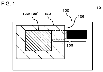
An organic EL element ( 102 ) is formed on a substrate ( 100 ), and an insulating layer ( 120 ) surrounds the organic EL element ( 102 ).
US 9,847,229 B2 · Assignee: Infineon Technologies AG · Inventors: Schulze; Hans-Joachim et al.
Sheet 1 of 33 from the published document. All sheets in the USPTO PDF
A method for forming a semiconductor device includes depositing an epitaxial layer on a semiconductor substrate, forming an oxygen diffusion region within the epitaxial layer by oxygen diffusion from the semiconductor substrate into a part of the epitaxial layer and tempering at least the oxygen diffusion region of the epitaxial layer at a temperature between 400° C. and 480° C. for more than 15 minutes.
The durability and life cycle of a semiconductor device is often affected by voltage peaks or current peaks during switch-off of the semiconductor device. For example, large currents can occur during the shutdown of power semiconductors. It is desired to decrease the risk of destruction due to high currents in order to increase the durability or life cycle of semiconductor devices, for example.
1 of 33 drawing sheets so far from the published document, cropped to the drawing. Every sheet is in the USPTO PDF.
What the patent claimed, word for word. All of it is now free to use.
This application claims priority to German Patent Application No. 10 2014 106 594.8 filed on 9 May 2014, the content said application incorporated herein by reference in its entirety.
Embodiments relate to measures for increasing the durability or life-cycle of semiconductor devices and in particular to a semiconductor device and a method for manufacturing a semiconductor device.
The durability and life cycle of a semiconductor device is often affected by voltage peaks or current peaks during switch-off of the semiconductor device. For example, large currents can occur during the shutdown of power semiconductors. It is desired to decrease the risk of destruction due to high currents in order to increase the durability or life cycle of semiconductor devices, for example.
There is a demand for providing a concept for increasing the durability or life cycle of semiconductor devices.
Such a demand may be satisfied by the subject matter of the claims.
Some embodiments relate to a method for forming a semiconductor device. The method comprises depositing an epitaxial layer on a semiconductor substrate and forming an oxygen diffusion region within the epitaxial layer by oxygen diffusion from the semiconductor substrate into a part of the epitaxial layer. Further, the method comprises tempering at least the oxygen diffusion region of the epitaxial layer at a temperature between 400° C. and 480° C. for more than 15 minutes.
Some embodiments relate to a method for forming a semiconductor device. The method comprises implanting oxygen into a semiconductor substrate and depositing an epitaxial layer on the semiconductor substrate. Further, the method comprises forming an oxygen diffusion region within the epitaxial layer by oxygen diffusion from the semiconductor substrate into a part of the epitaxial layer.
Some embodiments relate to a method for forming a semiconductor device. The method comprises depositing an epitaxial layer on a semiconductor substrate and forming an oxygen diffusion region within the epitaxial layer by oxygen diffusion from the semiconductor substrate into a part of the epitaxial layer. Further, the method comprises implanting hydrogen into the diffusion region of the epitaxial layer.
Some embodiments relate to a semiconductor device comprising an epitaxial substrate and a plurality of transistor structures or diode structures located at a front side of the epitaxial substrate. Further, the semiconductor device comprises a donor region located at a backside of the epitaxial substrate. The donor region comprises more than 10.sup.14 oxygen induced thermal donors per cm.sup.3 having a donor energy level between 30 meV and 200 meV.
Some embodiments relate to a semiconductor device comprising an epitaxial substrate with a donor region. The donor region comprises a laterally-varying oxygen concentration.
Those skilled in the art will recognize additional features and advantages upon reading the following detailed description, and upon viewing the accompanying drawings.
Some embodiments of apparatuses and/or methods will be described in the following by way of example only, and with reference to the accompanying figures, in which
FIG. 1 shows a flowchart of a method for forming a semiconductor device including tempering of the diffusion region;
FIG. 2 shows a flowchart of a method for forming a semiconductor device including implanting oxygen;
FIG. 3 shows a flowchart of a method for forming a semiconductor device including implanting hydrogen;
FIG. 4 shows a flowchart of a method for forming a semiconductor device including activating thermal donors;
FIGS. 5 a to 5 d show schematic cross-sections of the forming of a semiconductor device by the method shown in FIG. 4 ;
FIG. 6 shows a flowchart of a method for forming a semiconductor device including an oxygen implant;
FIGS. 7 a to 7 d show schematic cross-sections of the forming of a semiconductor device according to the method shown in FIG. 6 ;
FIG. 8 shows a flowchart of a method for forming a semiconductor device including a structured oxygen implant;
FIGS. 9 a to 9 e show schematic cross-sections of the forming of a semiconductor device according to the method shown in FIG. 8 ;
FIG. 10 shows a flowchart of a method for forming a semiconductor device including an additional temper process;
FIGS. 11 a to 11 f show schematic cross-sections of the forming of a semiconductor device according to the method shown in FIG. 10 ;
FIG. 12 shows a flowchart of a method for forming a semiconductor device including a hydrogen implant;
FIGS. 13 a to 13 f show schematic cross-sections of the forming of a semiconductor device according to the method shown in FIG. 12 ;
FIG. 14 shows a flowchart of a method for forming a semiconductor device;
FIG. 15 shows a schematic cross-section of a semiconductor device;
FIG. 16 shows a schematic cross-section of a semiconductor device;
FIG. 17 a shows a diffusion profile of oxygen at 1050° C. for 100 minutes and 1150° for 60 minutes with the interface to the carrier substrate at 0 μm;
FIG. 17 b shows another schematic diffusion profile of oxygen;
FIG. 18 shows the diffusion constant of oxygen (interstitial) in silicon; and
FIG. 19 shows the solubility of oxygen (interstitial) in silicon.
Various example embodiments will now be described more fully with reference to the accompanying drawings in which some example embodiments are illustrated. In the figures, the thicknesses of lines, layers and/or regions may be exaggerated for clarity.
Accordingly, while further embodiments are capable of various modifications and alternative forms, some example embodiments thereof are shown by way of example in the figures and will herein be described in detail. It should be understood, however, that there is no intent to limit example embodiments to the particular forms disclosed, but on the contrary, example embodiments are to cover all modifications, equivalents, and alternatives falling within the scope of the disclosure. Like numbers refer to like or similar elements throughout the description of the figures.
It will be understood that when an element is referred to as being “connected” or “coupled” to another element, it can be directly connected or coupled to the other element or intervening elements may be present. In contrast, when an element is referred to as being “directly connected” or “directly coupled” to another element, there are no intervening elements present. Other words used to describe the relationship between elements should be interpreted in a like fashion (e.g., “between” versus “directly between,” “adjacent” versus “directly adjacent,” etc.).
The terminology used herein is for the purpose of describing particular example embodiments only and is not intended to be limiting of further example embodiments. As used herein, the singular forms “a,” “an” and “the” are intended to include the plural forms as well, unless the context clearly indicates otherwise. It will be further understood that the terms “comprises,” “comprising,” “includes” and/or “including,” when used herein, specify the presence of stated features, integers, acts, operations, elements and/or components, but do not preclude the presence or addition of one or more other features, integers, acts, operations, elements, components and/or groups thereof.
Unless otherwise defined, all terms (including technical and scientific terms) used herein have the same meaning as commonly understood by one of ordinary skill in the art to which example embodiments belong. It will be further understood that terms, e.g., those defined in commonly used dictionaries, should be interpreted as having a meaning that is consistent with their meaning in the context of the relevant art and will not be interpreted in an idealized or overly formal sense unless expressly so defined herein.
FIG. 1 shows a flowchart of a method 100 for forming a semiconductor device according to an embodiment. The method 100 comprises depositing 110 an epitaxial layer on a semiconductor substrate and forming 120 an oxygen diffusion region within the epitaxial layer by oxygen diffusion from the semiconductor substrate into a part of the epitaxial layer. Further, the method 100 comprises tempering 130 at least the oxygen diffusion region of the epitaxial layer at a temperature between 400° C. and 480° C. for more than 15 minutes.
By implementing oxygen atoms into the epitaxial layer and tempering the resulting oxygen diffusion region, a region of thermal donors can be formed. The charge carrier mobility within the diffusion region may be reduced in comparison to the usage of other donors (e.g. phosphorus). In this way, the softness of the switching of semiconductor devices (e.g. switching-off of an insulated gate bipolar transistor or diode) may be improved. A semiconductor device with improved softness may comprise an increased durability or life cycle, for example.
The semiconductor substrate of the semiconductor device may be a silicon-based semiconductor substrate (e.g. CZ wafer or MCZ wafer), a silicon carbide-based semiconductor substrate, a gallium arsenide-based semiconductor substrate or a gallium nitride-based semiconductor substrate, for example.
The epitaxial layer may be deposited 110 on the semiconductor substrate by any epitaxial processing technology capable of forming an epitaxial layer on a given or desired semiconductor substrate. For example, the epitaxial layer may be a silicon layer, a silicon carbide layer, a gallium arsenide layer or a gallium nitride layer.
During and/or after the deposition of the epitaxial layer, oxygen atoms can diffuse from the semiconductor substrate to the epitaxial layer causing a region within increased oxygen concentration in comparison to other regions of the epitaxial layer. The oxygen diffusion is controllable in a well-defined manner by the oxygen concentration of the semiconductor substrate (e.g. of a surface region of the semiconductor substrate facing the epitaxial layer), the process temperatures and with it the oxygen solubility limit and processing time of the deposition of the epitaxial layer and/or manufacturing processes following the deposition 110 of the epitaxial layer, for example. In other words, the oxygen diffusion from the semiconductor substrate into the epitaxial layer may already start during the deposition 110 of the epitaxial layer.
At least the oxygen diffusion region (e.g. or the part of the semiconductor device already formed before the tempering) of the epitaxial layer is tempered or heated at a temperature between 400° C. and 480° C. (or between 420° C. and 470° C. or between 440° C. and 460° C., e.g. 450° C.) for more than 15 minutes (e.g. for more than 40 minutes and less than 30 hours, for more than one hour and less than 20 hours or for more than 5 hours and less than 15 hours). In the temperature range between 400° C. and 480° C., the forming of long oxygen chains may be triggered. Such long oxygen chains within the epitaxial layer may form thermal donors with at least a donor energy level between 30 meV and 200 meV (or between 40 meV and 100 meV, e.g. substantially 50 meV), for example. In other words, the epitaxial layer may be heated to a predefined temperature (or temperature range) for a predefined time in order to activate the thermal donor property of the oxygen atoms within the oxygen diffusion region, for example.
For example, an oxygen concentration within at least a part of the semiconductor substrate is larger than a solid state solubility of oxygen within the epitaxial layer, for example, at a maximum process temperature Tmax, during all following processing steps or at 1100° C. In this way, the in-diffusion of oxygen atoms into the substrate may be controlled in a very homogeneous and reproducible manner by the temperature dependency of the oxygen solubility limit. For example, FIG. 18 shows the oxygen diffusivity for different temperatures and FIG. 19 shows the oxygen solubility at different temperatures, as published in “Intrinsic point defects, impurities, and their diffusion in silicon”, P. Pichler, Springer, 2004.
The oxygen diffusion region may be a region of the epitaxial layer comprising a higher oxygen concentration than a remaining part of the epitaxial layer (e.g. more than twice or more than 10 times higher). The oxygen diffusion region may comprise a thickness (e.g. measured from a surface of the epitaxial layer into the epitaxial layer) of more than 1 μm (or more than 5 μm or more than 10 μm or a thickness between 1 μm and 100 μm, between 5 μm and 50 μm or between 10 μm and 30 μm), for example.
Optionally, processes following the tempering of the diffusion region may use temperatures below 400° C. In other words, process acts for forming the semiconductor device following the tempering of at least the diffusion region of the epitaxial layer at a temperature between 400° C. and 480° C. may be done mainly at temperatures below 400° C. For example, the following process acts may avoid temperatures above 400° C. for durations longer than one minute, for example. For example, all process acts for forming the semiconductor device following the tempering of the diffusion region may be performed completely below 400° C. In this way, a destructive effect to the oxygen chains formed during the tempering of the oxygen diffusion region or a further formation of thermal donors may be avoided or may be low. Alternatively or optionally, at least a part of the thermal donor annealing process at temperatures between 420° C. and 480° C. may be part of another process which requires or preforms an anneal step, for example.
The method 100 may comprise one or more additional optional acts corresponding to one or more aspects mentioned in connection with a described concept or one or more embodiments described below (e.g. implanting oxygen into the semiconductor substrate and/or implanting hydrogen into the oxygen diffusion region).
FIG. 2 shows a flowchart of a method 200 for forming a semiconductor device according to an embodiment. The method 200 comprises implanting 210 oxygen into a semiconductor substrate and depositing 110 an epitaxial layer on the semiconductor substrate. Further, the method comprises forming 120 an oxygen diffusion region within the epitaxial layer by oxygen diffusion from the semiconductor substrate into a part of the epitaxial layer.
By implanting oxygen into the semiconductor substrate, an oxygen concentration within the semiconductor substrate can be increased to a desired concentration. In this way, the amount of oxygen diffusing into the epitaxial layer can be influenced. The oxygen diffusion region may build up a region of thermal donors with a desired donor concentration due to the controllable amount of oxygen diffusing into the epitaxial layer. In this way, the softness of the switching of the semiconductor device may be improved.
The implant 210 of oxygen ions into the semiconductor substrate may be done with low implant energy so that the oxygen concentration is increased within a surface region (e.g. extending from a surface of the semiconductor substrate into the semiconductor substrate) of the semiconductor substrate.
The oxygen implant may be done throughout the whole surface of the semiconductor substrate or may be done at a part of the surface of the semiconductor substrate only. For example, an implant window of the ion implanter may be reduced to a desired part of the semiconductor substrate (e.g. semiconductor wafer) so that the desired part of the semiconductor substrate is exposed to the oxygen implant only. Alternatively, a mask layer may be formed on the surface of the semiconductor substrate (e.g. photoresist layer) to mask or avoid the oxygen implant at desired regions of the semiconductor substrate. In this way, a lateral variation of the oxygen concentration within the semiconductor substrate may be achievable, for example.
Afterwards, the oxygen diffusion region may be formed by oxygen diffusion from the semiconductor substrate with laterally varying oxygen concentration resulting in an oxygen diffusion region with laterally varying oxygen concentration. For example, at a predefined distance from a surface of the epitaxial layer, a maximal oxygen concentration of the oxygen diffusion region may be higher than twice (or higher than ten times) a minimal oxygen concentration at the predefined distance.
In this way, an alternating sequence of first concentration regions and second concentration regions distributed laterally in a direction along a surface of the semiconductor substrate may be obtained.
Optionally, an oxygen concentration of the semiconductor substrate is measured before the oxygen implant. In this way, the already existing oxygen concentration within the semiconductor substrate can be considered for the determination of the oxygen dose to be implanted in order to obtain a desired resulting oxygen concentration at least at a surface region of the semiconductor substrate, for example.
More details regarding the deposition 110 of the epitaxial layer and for forming 120 the oxygen diffusion region within the epitaxial layer are mentioned in connection with FIG. 1 or one or more embodiments described below.
The method 200 may comprise one or more additional optional acts corresponding to one or more aspect(s) mentioned in connection with a described concept or one or more embodiments described above or below (e.g. tempering the diffusion region at the temperature between 400° C. and 480° C. for more than 15 minutes and/or implanting hydrogen into the diffusion region).
FIG. 3 shows a method 300 for forming a semiconductor device according to an embodiment. The method 300 comprises depositing 110 an epitaxial layer on a semiconductor substrate and forming 120 an oxygen diffusion region within the epitaxial layer by oxygen diffusion from the semiconductor substrate into a part of the epitaxial layer. Further, the method 300 comprises implanting 330 hydrogen into the oxygen diffusion region of the epitaxial layer.
By implanting hydrogen ions into the oxygen diffusion region, the growth of oxygen chains may be catalyzed or stimulated by the hydrogen. For example the process time for tempering the oxygen diffusion region at a temperature between 400° C. and 480° C. may be reduced or the tempering process may be avoided due to the catalyzing effect of the hydrogen within the oxygen diffusion region, for example. In this way, the generation of thermal donors represented by oxygen within the oxygen diffusion region may be improved. The switching behavior of the semiconductor device may be smoothed due to the thermal donors. In this way, the durability and/or the lifecycle of the semiconductor device may be increased.
The hydrogen may be implanted 330 with an implant energy suitable for implanting hydrogen into the oxygen diffusion region of the epitaxial layer. Alternatively or additionally, a hydrogen in-diffusion step may be performed (e.g. by a plasma supplied in-diffusion)
Optionally, an additional annealing act may be performed to improve the catalyzing effect of the hydrogen within the oxygen diffusion region (e.g. to remove any (parasitic) H-rel thermal donors induced by the H implant). In other words, the method 300 may comprise tempering or heating at least an oxygen diffusion region of the epitaxial layer at a temperature between 500° C. and 600° C. for more than 15 minutes after the hydrogen implant.
More details in connection with depositing 110 the epitaxial layer and forming 120 the oxygen diffusion region are mentioned in connection with FIG. 1 and/or one or more embodiments described below, for example.
The method 300 may comprise one or more additional optional acts corresponding to one or more aspects mentioned in connection with a described concept or one or more embodiments described above or below (e.g. tempering the oxygen diffusion region at a temperature between 400° C. and 480° C. for more than 15 minutes and/or implanting oxygen into the semiconductor substrate).
As already mentioned, the diffusion process of the oxygen from the semiconductor substrate to the epitaxial layer may already start during the deposition 110 of the epitaxial layer. For example, depositing 110 the epitaxial layer on the semiconductor substrate may be at least partly done at a first temperature range above 1000° C. (e.g. 1050° C. for 100 minutes or another temperature and time depending on the semiconductor device to be formed) causing at least a part of the oxygen diffusion from the semiconductor substrate into a part of the epitaxial layer forming the oxygen diffusion region within the epitaxial layer. The first temperature range may be defined by a single temperature above 1000° C. for a predefined time or may be defined by a varying temperature profile comprising different temperatures above 1000° C. at different times, for example.
Optionally, a method described above may further comprise forming field-effect transistor structures at a front side of the semiconductor device. In other words, field-effect transistor structures may be formed at a surface of the epitaxial layer opposite to the semiconductor substrate (e.g. carrier substrate) or at a layer deposited on the epitaxial layer, for example.
The front side of the semiconductor device may be a side of the semiconductor device comprising more complex structures than a backside of the semiconductor device. For example, the field-effect transistor structures (e.g. especially the gate of a field-effect transistor) of an IGBT may be located at the front side of a semiconductor device, while an emitter may be located at a backside of the insulated gate bipolar transistor.
The IGBT transistor or the field-effect transistor structures may be n-channel field-effect transistor structures.
The oxygen diffusion region of the epitaxial layer may form a field stop region of an insulated gate bipolar transistor (e.g. layer between a backside emitter and a drift region), for example.
The forming of the field-effect transistor structures may be at least partly done at a second temperature range being higher than a first temperature range. In this way, further oxygen may diffuse from the semiconductor substrate to the epitaxial layer. For example, the second temperature range may comprise one or more temperatures for one or more different times. For example, at least one temperature of the second temperature range may be above 1050° C. (e.g. 1100° C.).
A method described above may further comprise optionally an additional tempering of at least the oxygen diffusion region of the epitaxial layer at a third temperature range being higher than the second temperature range. In this way, the oxygen diffusion from the semiconductor substrate to the epitaxial layer may be influenced independent from the deposition of the epitaxial layer and/or the forming of the field-effect transistor structures to obtain a desired oxygen concentration or oxygen distribution within the oxygen diffusion region, for example. The additional tempering of the oxygen diffusion region at the third temperature range may be done before or after forming the field-effect transistor structures, for example.
A method described above may further comprise forming an emitter layer at the backside of the semiconductor device. In this way, an insulated gate bipolar transistor may be manufactured, for example.
FIG. 4 shows a flowchart of a method 400 for forming a semiconductor device. The process overview indicates an epitaxial growth 408 of the active volume (e.g. temperature process T 1 ) representing the deposition of the epitaxial layer mentioned above and processing 412 of the device front side including temperature process T 2 (e.g. transistor cell and/or edge termination, forming a field-effect transistor structure or an anode region). Further, the method 400 comprises thinning 414 from the backside of the carrier substrate representing the semiconductor substrate (e.g. by using previously-implemented trenches as chemical-mechanical polishing CMP stops) and processing 416 of the device backside (e.g. p+ emitter implant). Additionally, the method 400 comprises a temperature process 420 for activating the thermal donors (e.g. 400° C., 5 hours), an optional thin wafer process (thinning of wafer), a processing 422 of the device front side (e.g. metallization and/or imide) and a back end BE process 424 including metallization of the backside. In this way a diode and/or an insulated gate bipolar transistor may be formed, for example. Further, the flowchart indicates further optional acts, which are described in connection with one or more examples below.
FIGS. 5 a to 5 d show schematic cross-sections of a semiconductor device during forming the semiconductor device according to the method shown in FIG. 4 . FIG. 5 a shows the carrier substrate 510 with an oxygen concentration C.sub.O above the maximum solid state solubility S.sub.O(T.sub.max) of the following process. FIG. 5 b shows the epitaxial growth of the active device volume 520 (e.g. at a thermal budget T 1 of 1050° C. for 100 minutes for a 1200 V device, for example). Oxygen diffuses into the active volume 520 (into the epitaxial layer or substrate) during the process corresponding the diffusion constant D(T) of oxygen and the solid state solubility S(T) of oxygen, for example.
Consequently, an oxygen diffusion region 522 is formed within the epitaxial layer 520 by oxygen diffusion from the semiconductor substrate 510 into the epitaxial substrate 520 .
FIG. 5 c shows the processing of the device front side (e.g. insulated gate bipolar transistor IGBT transistor cells 530 ) including a p-body drive T 2 (e.g. at 1100° C.). The p-body drive may be a temperature process for annealing or diffusing the doping of the field-effect transistor structure (e.g. after p implant). Due to the usage of temperatures within a second temperature range T 2 , the oxygen diffusion region 522 expands further into the epitaxial layer 520 .
FIG. 5 d shows the semiconductor device after grinding the wafer (e.g. removal of the carrier substrate) and implantation of the backside p+ emitter 540 . Optionally, the thinning of the wafer is done by using CMP stop structures. Further, an activating process of the oxygen thermal donors OTD based on the controlled generated oxygen profile is performed.
The method 400 may comprise one or more additional optional acts corresponding to one or more aspects mentioned in connection with the described concept or one or more embodiments described above or below.
FIG. 6 shows a flowchart of a method 430 for forming a semiconductor device according to an embodiment. The process overview comprises an optional measurement 402 of the oxygen concentration of the carrier substrate (semiconductor substrate). Further, the method 430 comprises an oxygen implant 404 into the carrier substrate (e.g. optionally with dose adaptations corresponding to the starting oxygen concentration) and an epitaxial growth 408 of the active volume (e.g. by temperature process T 1 ). Additionally, the method 430 comprises processing 412 of the device front side including temperature process T 2 (e.g. transistor cells, etch termination and/or field-effect transistor structures) and a thinning of the backside of the carrier substrate 414 (e.g. by using previously-implemented trenches as CMP stops). Further, the method 430 comprises processing 416 the device front side (e.g. p+ emitter implant) and a temperature process 420 for activating the thermal donors (e.g. 400° C., 5 hours). Additionally, the method 430 comprises an optional wafer thinning, a processing 422 of the device front side (e.g. metallization, imide) and a back end BE processing 424 including a metallization of the backside. Further, the flowchart of FIG. 6 indicates additional optional acts which are described in connection with one or more examples above or below.
FIGS. 7 a to 7 d show schematic cross-sections of the forming of a semiconductor device according to the method shown in FIG. 6 . FIG. 7 a shows an oxygen implant into a carrier substrate (semiconductor substrate) 510 . In this way, a surface region 712 with increased oxygen concentration C.sub.O,1, may be formed. Optionally, the oxygen implant may be done with a dose adaptation depending on the oxygen concentration C.sub.O of the (remaining) carrier substrate, for example.
FIG. 7 b shows an epitaxial growth of the active device volume 520 (e.g. at a thermal budget T 1 of, for example, 1050° C. for 100 minutes for a 1200 V device). During the deposition of the epitaxial substrate, oxygen diffuses into the active volume according to the diffusion constant D(T) of oxygen and the solid state solubility S(T). In this way, an oxygen diffusion region 522 with an oxygen concentration C.sub.O(T 1 )<C.sub.O,1 may be formed.
FIG. 7 c shows the processing of the device front side (e.g. IGBT transistor cells) including a P body drive (e.g. at 1100° C.) resulting in an oxygen diffusion region 522 with an oxygen concentration C.sub.O(T 2 )≦C.sub.O,1, for example.
FIG. 7 d shows the semiconductor device after grinding the wafer (e.g. removal of the carrier substrate) and implantation of the backside p+ emitter 540 . Optionally, the thinning of the wafer is done by using CMP stop structures. Further, an activating process of the oxygen thermal donors OTD based on the controlled generated oxygen profile is performed.
The method 430 may comprise one or more additional optional acts corresponding to one or more aspect described in connection with a concept or one or more embodiments described above or below.
FIG. 8 shows a flowchart of a method 440 for forming a semiconductor device according to an embodiment. The method 440 is similar to the method shown in FIG. 6 , but comprises additionally a structured oxygen implant 406 . Further, the flowchart of FIG. 8 indicates additional optional acts which are described in connection with one or more examples above or below.
FIGS. 9 a to 9 e show schematic cross-sections of the forming a semiconductor device according to the method of FIG. 8 . FIG. 9 a shows an oxygen implant into a carrier substrate (semiconductor substrate) 510 .
FIG. 9 b shows a structured second oxygen implant into the carrier substrate, which is a masked oxygen implant. In this way, a laterally-varying oxygen concentration may be obtained in a surface region of the carrier substrate.
In this way, an alternating sequence of first concentration regions 914 and second concentration regions 916 distributed laterally in a direction along a surface of the semiconductor substrate may be obtained.
FIG. 9 c shows an epitaxial growth of the active device volume 520 (e.g. at a thermal budget T 1 of, for example, 1050° C. for 100 minutes for a 1200 V device). During the deposition of the epitaxial substrate, oxygen diffuses into the active volume according to the diffusion constant D(T) of oxygen and the solid state solubility S(T). After the epitaxial growth of the epitaxial layer 520 , the oxygen diffusion region 522 may comprise an oxygen concentration C.sub.O(T 1 )≦C.sub.O,1<C.sub.O,2 for example.
FIG. 9 d shows the processing of the device front side (e.g. IGBT transistor sets) including a p-body drive (e.g. at 1100° C.). After the processing of the device front side, the oxygen diffusion region 522 within the epitaxial layer 520 may comprise a laterally varying oxide concentration (e.g. C.sub.O,1<C.sub.O(T 2 )≦C.sub.O,2).
FIG. 9 e shows the semiconductor device after grinding the wafer (e.g. removal of the carrier substrate) and implantation of the backside p+ emitter 540 . Optionally, the thinning of the wafer is done by using CMP stop structures. Further, an activating process of the oxygen thermal donors OTD based on the controlled generated oxygen profile is performed.
The method 440 may comprise one or more additional optional acts corresponding to one or more aspect described in connection with a concept or one or more embodiments described above or below.
FIG. 10 shows a method 450 for forming a semiconductor device according to an embodiment. The method 450 is similar to the method shown in FIG. 8 , but comprises additionally a further temperature process 410 (e.g. inert) at a third temperature or temperature range T 3 (e.g. T 1 <T 2 <T 3 or T 1 <T 3 <T 2 ). FIG. 10 indicates a further optional act, which may be used by one or more other examples mentioned above or below.
FIGS. 11 a to 11 f show schematic cross-sections of the forming of the semiconductor device according to the method shown in FIG. 10 . FIG. 11 a shows an oxygen implant into a carrier substrate (semiconductor substrate) 510 .
FIG. 11 b shows a structured second oxygen implant into the carrier substrate, which is a masked oxygen implant. In this way, a laterally-varying oxygen concentration may be obtained in a surface region of the carrier substrate.
FIG. 11 c shows an epitaxial growth of the active device volume 520 (e.g. at a thermal budget T 1 of, for example, 1050° C. for 100 minutes for a 1200 V device). During the deposition of the epitaxial substrate, oxygen diffuses into the active volume according to the diffusion constant D(T) of oxygen and the solid state solubility S(T). After the epitaxial growth of the epitaxial layer 520 , the oxygen diffusion region 522 may comprise an oxygen concentration C.sub.O(T 1 )≦C.sub.O,1<C.sub.O,2 for example.
FIG. 11 d shows an additional tempering at temperature or temperature range T 3 . The additional oxygen drive at temperature or temperature range T 3 (e.g. inert) may be done subsequently to the epitaxy. For example, T 1 <T 2 <T 3 . Oxygen diffuses during this process according to the diffusion constant D(T) of oxygen and the solid state solubility S(T) of oxygen into the active volume. In this way, an oxygen diffusion region 522 with an oxygen concentration of C.sub.O,1<C.sub.O(T 3 )≦C.sub.O,2 may be obtained, for example.
FIG. 11 e shows the processing of the device front side (e.g. IGBT transistor sets) including a p-body drive (e.g. at 1100° C.). After the processing of the device front side, the oxygen diffusion region 522 within the epitaxial layer 520 may comprise a laterally varying oxide concentration (e.g. C.sub.O,1<C.sub.O(T 2 )≦C.sub.O,2).
FIG. 11 f shows the semiconductor device after grinding the wafer (e.g. removal of the carrier substrate) and implantation of the backside p+ emitter 540 . Optionally, the thinning of the wafer is done by using CMP stop structures. Further, an activating process of the oxygen thermal donors OTD based on the controlled generated oxygen profile is performed.
The method 450 may comprise one or more additional optional acts corresponding to one or more aspects mentioned in connection with a concept or one or more embodiments described above or below.
FIG. 12 shows a flowchart of a method 460 for forming a semiconductor device according to an embodiment. The method 460 is similar to the method shown in FIG. 4 , but comprises additionally a hydrogen implant 480 (e.g. including optionally a thermal process for hydrogen diffusion and hydrogen thermal donor HTD elimination above, e.g., 500° C. for one hour, for example), which may be performed after the processing 416 of the device backside and before the temperature process 420 for activating the thermal donors of the oxygen. FIG. 12 indicates further optional acts, which may be used by one or more methods described above or below.
FIGS. 13 a to 13 f show a schematic cross-section of the forming of a semiconductor device according to the method shown in FIG. 12 . FIG. 13 a shows the carrier substrate 510 with an oxygen concentration C.sub.O above the maximum solid state solubility S.sub.O(T.sub.max) of the following process. FIG. 13 b shows the epitaxial growth of the active device volume 520 (e.g. at a thermal budget T 1 of 1050° C. for 100 minutes for a 1200 V device, for example). Oxygen diffuses into the active volume 520 (into the epitaxial layer or substrate) during the process corresponding the diffusion constant D(T) of oxygen and the solid state solubility S(T) of oxygen, for example.
Consequently, an oxygen diffusion region 522 is formed within the epitaxial layer 520 by oxygen diffusion from the semiconductor substrate 510 into the epitaxial substrate 520 .
FIG. 13 c shows the processing of the device front side (e.g. insulated gate bipolar transistor IGBT transistor cells 530 ) including a p-body drive T 2 (e.g. at 1100° C.). The p-body drive may be a temperature process for annealing or diffusing the doping of the field-effect transistor structure (e.g. after p implant). Due to the usage of temperatures within a second temperature range T 2 , the oxygen diffusion region 522 expands further into the epitaxial layer 520 .
FIG. 13 d shows the thinning of the wafer (e.g. removal of the carrier substrate) and the implantation of the backside P emitter. Optionally, CMP stop structures may be used for the thinning, for example.
FIG. 13 e shows the implant of hydrogen (e.g. including hydrogen thermal donors kill process). A buried hydrogen implant may be performed followed by an optional hydrogen diffusion act. Alternatively or additionally, an annealing act to anneal out hydrogen correlated donors (HTD) at 550° C. for one hour may be done, for example, for hydrogen doses above 10.sup.13 cm.sup.2. By implanting hydrogen into the oxygen diffusion region 522 , a region of increased hydrogen concentration 1324 may be obtained. This region 1324 may be expanded by a diffusion process. The hydrogen may catalyze the growth of large oxygen chains building up thermal donors, for example. Alternatively or in addition, an annealing step at 350-500° C. for 1-10 h, e.g., at 400-490° C. for 1-5 h, e.g., at 400° C. for 1-4 h may be performed to induce H-rel thermal donors, for example.
FIG. 13 f shows the semiconductor device after grinding the wafer (e.g. removal of the carrier substrate) and implantation of the backside p+ emitter 540 . Optionally, the thinning of the wafer is done by using CMP stop structures. Further, an activating process of the oxygen thermal donors OTD based on the controlled generated oxygen profile is performed.
The method 460 may comprise one or more additional optional acts corresponding to one or more aspects described in connection with a concept or one or more embodiments described above or below.
FIG. 14 shows a flowchart of a method 470 according to an embodiment. The method 470 comprises a combination of process acts of the methods described in connection with FIGS. 1 to 13 f.
Details regarding the different processes of the method 470 are described in connection with embodiments above or below.
Some embodiments relate to a semiconductor diode device (e.g. silicon diode or silicon carbide diode) or a semiconductor field effect transistor device (e.g. reverse-blocking or reverse-conduction insulated gate bipolar transistor) or a method for forming a semiconductor diode device or a semiconductor field effect transistor device. In other words, a semiconductor device according to the described concept or one more embodiments described above may implement a semiconductor diode device or a semiconductor field effect transistor device, for example.
The oxygen diffusion region of the epitaxial layer may form a field stop region of an insulated gate bipolar transistor (e.g. layer between a backside emitter and a drift region), for example.
Some embodiments relate to a power semiconductor device. In other words, a semiconductor device according to the described concept or one or more embodiments described above may comprise a blocking voltage of more than 100 V (e.g. between 100 V and 10000 V or more than 500 V, more than 1000 V or more than 4000 V).
The description continues in the full USPTO document.
About 6,412 words. The USPTO PDF has it with every drawing.
Fees are due 3.5, 7.5 and 11.5 years after grant. This patent expired on December 19, 2025, so the fee marked "not paid" was the one that went unpaid.
Method for Forming a Semiconductor Device and Semiconductor Device
Filed May 2015 · published Nov 2015Method for forming a semiconductor device and semiconductor device
Filed May 2015 · granted Dec 2017Earlier publications, parents and continuations. None of them can still be enforced, or this patent would not be listed.
Prior art cited by the examiner or applicant. Useful when you check your own idea for novelty.
Everything on this page comes from the documents linked above.