Cross-reference to related applications
This application claims the benefit under 35 USC 119(a) of Korean Patent Application No. 10-2013-0111090 filed on Sep. 16, 2013, in the Korean Intellectual Property Office, the entire disclosure of which is incorporated herein by reference for all purposes.
Background
1.
Field
The following description relates to a wireless power transmission system.
2. Description of related art
Wireless power is energy that is transmitted from a wireless power transmitter to a wireless power receiver via magnetic coupling. A wireless power charging system includes a source device and a target device. The source device wirelessly transmits power, and the target device wirelessly receives power. The source device may be referred to as a wireless power transmitter, and the target device may be referred to as a wireless power receiver.
The source device includes a source resonator, and the target device includes a target resonator. Magnetic coupling or resonance coupling occurs between the source resonator and the target resonator.
Summary
This Summary is provided to introduce a selection of concepts in a simplified form that are further described below in the Detailed Description. This Summary is not intended to identify key features or essential features of the claimed subject matter, nor is it intended to be used as an aid in determining the scope of the claimed subject matter.
In one general aspect, a resonating apparatus for wireless power transmission includes a plurality of resonators separated from each other on a same plane; and a material configured to reduce resonance coupling among the plurality of resonators.
The material may be disposed between each of the plurality of resonators and an adjacent resonator of the plurality of resonators.
The material may be disposed on a plane opposite to a direction in which the plurality of resonators are configured to resonate.
The material may include either one or both of a magnetic material and a conductor.
In another general aspect, a resonating apparatus includes a plurality of resonators disposed on a same plane; wherein at least one of the plurality of resonators is disposed to overlap a portion of an adjacent resonator of the plurality of resonators to reduce resonance coupling with the adjacent resonator.
The plurality of resonators may be disposed to reduce resonance coupling between each of the plurality of resonators and an adjacent resonator of the plurality of resonators based on a characteristic that a direction of a magnetic field of an overlapping area in each of the plurality of resonators in which each of the plurality of resonators overlaps the adjacent resonator is opposite to a direction of a magnetic field of a non-overlapping area in each of the plurality of resonators in which each of the plurality of resonators does not overlap the adjacent resonator.
The plurality of resonators may be disposed to minimize an H-field surface integral value of each of the plurality of resonators.
At least one of the plurality of resonators may be divided into two areas having mutual fluxes in opposite directions, the two areas being disposed to cause absolute values of the mutual fluxes of the two areas to be equal to one another or within a predetermined range of one another.
The plurality of resonators may include at least three resonators.
In another general aspect, a transmission resonating apparatus includes a plurality of transmission resonators disposed on a same plane, each of the plurality of transmission resonators being configured to form a resonant mode with an adjacent transmission resonator among the plurality of transmission resonators; and a feeder configured to inject power into the plurality of transmission resonators at an operating frequency set to decrease coupling between each of the plurality of transmission resonators and the adjacent transmission resonator based on the resonant mode.
A difference between the operating frequency and a frequency corresponding to the resonant mode is than or equal to a predetermined value.
The resonant mode may include either one or both of an even mode in which a magnetic field generated in each of the plurality of transmission resonators and a magnetic field generated in the adjacent transmission resonator have a same direction, and an odd mode in which the magnetic field generated in each of the plurality of transmission resonators and the magnetic field generated in the adjacent transmission resonator have opposite directions.
The resonant mode may be the even mode; and a difference between the operating frequency and a frequency corresponding to the even mode may be less than or equal to a predetermined value.
The resonant mode may be the odd mode; and a difference between the operating frequency and a frequency corresponding to the odd mode may be less than or equal to a predetermined value.
The plurality of transmission resonators may be connected in parallel with each other; and the feeder may be connected in series with the plurality of transmission resonators connected in parallel with each other to inject power at the set operating frequency into the plurality of transmission resonators.
The plurality of transmission resonators may be connected in series with each other; and the feeder may be connected in parallel with the plurality of transmission resonators connected in series with each other to inject power at the set operating frequency into the plurality of transmission resonators.
The feeder may be further configured to inject power at the set operating frequency into the plurality of transmission resonators via inductive coupling.
In another general aspect, a resonating apparatus includes a plurality of resonators disposed in a same plane and configured so that each of the plurality of resonators is able to generate a magnetic field independently without being influenced by any other magnetic field generated by any other one of the plurality of resonators.
The resonating apparatus may further include an isolating material; and the plurality of resonators may be disposed so that the isolating material isolates each of the plurality of resonators from a magnetic field generated by every other one of the plurality of resonators.
Each of the plurality of resonators may include a non-overlapping area in which the resonator does not overlap any other one of the plurality of resonators, and an overlapping area in which the resonator overlaps every other one of the plurality of resonators that is adjacent to the resonator; and a size of the non-overlapping area and a size of the overlapping area may be selected to minimize an H-field surface field integral of the resonator.
Other features and aspects will be apparent from the following detailed description, the drawings, and the claims.
Brief description of the drawings
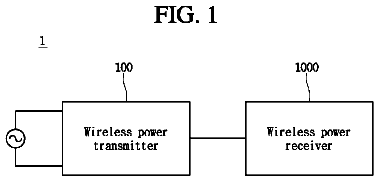
FIG. 1 illustrates an example of a wireless power and reception transmission system.
FIGS. 2A and 2B illustrate examples of a distribution of a magnetic field in a feeder and a resonator.
FIGS. 3A and 3B illustrate an example of a wireless power transmitter.
FIG. 4A illustrates an example of a distribution of a magnetic field inside a resonator produced by feeding a feeder.
FIG. 4B illustrates examples of equivalent circuits of a feeder and a resonator.
FIG. 5 illustrates an example of an electric vehicle charging system.
FIGS. 6A, 6B, 7A, and 7B illustrate examples of applications using a wireless power receiver and a wireless power transmitter.
FIG. 8 illustrates an example of a wireless power receiver and a wireless power transmitter.
FIG. 9 illustrates an example of a wireless power transmission system including a wireless power transmitter including a feeder and a plurality of transmission resonators, and a wireless power receiver including a plurality of reception resonators.
FIG. 10 illustrates an example of a wireless power transmission system including a wireless power transmitter in which a plurality of feeders are respectively connected to a plurality of transmission resonators, and a wireless power receiver including a plurality of reception resonators.
FIG. 11 illustrates an example of a structure in which each of a plurality of transmission resonators is strongly coupled to adjacent ones of the plurality of transmission resonators.
FIG. 12 illustrates an example of a structure in which a plurality of resonators are weakly coupled to each other through either one or both of a magnetic material and a conductor.
FIGS. 13A and 13B illustrate another example of a structure in which a plurality of resonators are weakly coupled to each other through either one or both of a magnetic material and a conductor.
FIG. 14 illustrates an example of a structure in which resonators in a plurality of overlapping resonators are weakly coupled to each other.
FIG. 15 illustrates an example of resonant modes generated by each of a plurality of transmission resonators and an adjacent transmission resonator.
FIGS. 16 through 18 illustrate examples of methods of connecting a plurality of transmission resonators to a feeder.
FIG. 19 illustrates an example of a configuration of a wireless power transmitter and a wireless power receiver.
Detailed description
The following detailed description is provided to assist the reader in gaining a comprehensive understanding of the methods, apparatuses, and/or systems described herein. However, various changes, modifications, and equivalents of the methods, apparatuses and/or systems described herein will be apparent to one of ordinary skill in the art. The sequences of operations described herein are merely examples, and are not limited to those set forth herein, but may be changed as will be apparent to one of ordinary skill in the art, with the exception of operations necessarily occurring in a certain order. Also, descriptions of functions and constructions that are well known to one of ordinary skill in the art may be omitted for increased clarity and conciseness.
Throughout the drawings and the detailed description, the same reference numerals refer to the same elements. The drawings may not be to scale, and the relative size, proportions, and depiction of elements in the drawings may be exaggerated for clarity, illustration, and convenience.
Schemes of performing communication between a source and a target include an in-band communication scheme and an out-of-band communication scheme. The in-band communication scheme is communication performed between the source and the target in the same frequency band that is used for power transmission. The out-of-band communication scheme is communication performed between the source and the target in a frequency band that is different from a frequency band used for power transmission.
FIG. 1 illustrates an example of a wireless power transmission and reception system.
Referring to FIG. 1 , the wireless power transmission system and reception includes a source 110 and a target 120 . The source 110 is a device configured to supply wireless power, and may be any electronic device capable of supplying power, such as, for example, a pad, a terminal, a table personal computer (PC), a television (TV), a medical device, or an electric vehicle. The target 120 is a device configured to receive wireless power, and may be any electronic device requiring power to operate, such as, for example, a pad, a terminal, a tablet PC, a TV, a smart watch, a medical device, an electric vehicle, a washing machine, a radio, or a lighting system.
The source 110 includes a variable switching mode power supply (SMPS) 111 , a power amplifier (PA) 112 , a matching network 113 , a transmission (TX) controller 114 , such as, for example, TX control logic, a communication unit 115 , and a power detector 116 .
The variable SMPS 111 generates a direct current (DC) voltage by switching an alternating current (AC) voltage having a frequency of tens of hertz (Hz) output from a power supply. The variable SMPS 111 may output a fixed DC voltage having a predetermined level, or may output an adjustable DC voltage having an adjustable level under the control of the TX controller 114 .
The power detector 116 detects an output current and an output voltage of the variable SMPS 111 , and provides, to the TX controller 114 , information on the detected output current and the detected output voltage. Also, the power detector 116 detects an input current and an input voltage of the power amplifier 112 .
The power amplifier 112 generates power by converting a DC voltage having a predetermined level supplied to the power amplifier 112 by the variable SMPS 111 to an AC voltage using a switching pulse signal having a frequency of a few megahertz (MHz) to tens of MHz. For example, the power amplifier 112 may convert the DC voltage supplied to the power amplifier 112 to an AC voltage having a reference resonant frequency F.sub.Ref, and may generate communication power used for communication, and/or charging power used for charging. The communication power and the charging power may be used in a plurality of targets.
The communication power may be a low power of 0.1 milliwatt (mW) to 1 mW. The charging power may be a high power of 1 mW to 200 W that is consumed by a load of a target. As used herein, the term “charging” refers to supplying power to a unit or element configured to charge a battery or other rechargeable device with power. Additionally, the term “charging” may refer to supplying power to a unit or element configured to consume power. The units or elements may be, for example, a battery, a display, a sound output circuit, a main processor, or any of various types of sensors.
As used herein, the term “reference resonant frequency” refers to a resonant frequency nominally used by the source 110 , and the term “tracking frequency” refers to a resonant frequency used by the source 110 that has been adjusted based on a preset scheme.
The TX controller 114 detects a reflected wave of the communication power or the charging power, and detects mismatching that occurs between a target resonator 133 and a source resonator 131 based on the detected reflected wave. To detect the mismatching, for example, the TX controller 114 may detect an envelope of the reflected wave, a power amount of the reflected wave, or any other characteristic of the reflected wave that is affected by mismatching.
The matching network 113 compensates for impedance mismatching between the source resonator 131 and the target resonator 133 to achieve optimal matching under the control of the TX controller 114 . The matching network 113 includes a plurality of switches each connected to a capacitor or an inductor, and the switches are controlled by the TX controller 114 to achieve optimal matching.
The TX controller 114 calculates a voltage standing wave ratio (VSWR) based on a voltage level of the reflected wave and a level of an output voltage of the source resonator 131 or the power amplifier 112 . For example, when the VSWR is greater than a predetermined value, the TX controller 114 detects that there is mismatching between the source resonator 131 and the target resonator 133 .
When the TX controller 114 detects that the VSWR is greater than the predetermined value, the TX controller 114 may compute a wireless power transmission efficiency for each of N tracking frequencies, determine a tracking frequency F.sub.Best providing the best wireless power transmission efficiency among the N tracking frequencies, and change the reference resonant frequency F.sub.Ref to the tracking frequency F.sub.Best. The N tracking frequencies may be set in advance.
The TX controller 114 may adjust a frequency of the switching pulse signal used by the power amplifier 112 . The frequency of the switching pulse signal may be determined under the control of the TX controller 114 . For example, by controlling the frequency of the switching pulse signal used by the power amplifier 112 , the TX controller 114 may generate a modulated signal to be transmitted to the target 120 . In other words, the TX controller 114 may transmit a variety of data to the target 120 using in-band communication. The TX controller 114 may also detect a reflected wave, and may demodulate a signal received from the target 120 based on an envelope of the detected reflected wave.
The TX controller 114 may generate a modulated signal for in-band communication using various methods. For example, the TX controller 114 may generate the modulated signal by turning on or off a switching pulse signal used by the power amplifier 112 , by performing delta-sigma modulation or by any other modulation method known to one of ordinary skill in the art. Additionally, the TX controller 114 may generate a pulse-width modulated (PWM) signal having a predetermined envelope.
The communication unit 115 may perform out-of-band communication using a separate communication channel. The communication unit 115 may include a communication module, such as a ZigBee module, a Bluetooth module, or any other communication module known to one of ordinary skill in the art that the communication unit 115 may use to transmit and receive data 140 to and from the target 120 via the out-of-band communication.
The source resonator 131 transfers electromagnetic energy 130 to the target resonator 133 . For example, the source resonator 131 transfers the communication power or the charging power to the target 120 via magnetic coupling with the target resonator 133 .
As illustrated in FIG. 1 , the target 120 includes a matching network 121 , a rectifier 122 , a DC/DC converter 123 , a communication unit 124 , a reception (RX) controller 125 , such as, for example, RX control logic, a voltage detector 126 , and a power detector 127 .
The target resonator 133 receives the electromagnetic energy 130 from the source resonator 131 . For example, the target resonator 133 receives the communication power or the charging power from the source 110 via magnetic coupling with the source resonator 131 . Additionally, the target resonator 133 may receive a variety of data from the source 110 via the in-band communication.
The matching network 121 matches an input impedance viewed from the source 110 to an output impedance viewed from a load of the target 120 . The matching network 121 may be configured to have at least one capacitor and at least one inductor.
The rectifier 122 generates a DC voltage by rectifying an AC voltage received by the target resonator 133 .
The DC/DC converter 123 adjusts a level of the DC voltage generated by the rectifier 122 based on a voltage required by the load. As an example, the DC/DC converter 123 may adjust the level of the DC voltage output from the rectifier 122 to a level in a range of 3 volts (V) to 10 V.
The voltage detector 126 detects a voltage of an input terminal of the DC/DC converter 123 , and the power detector 127 detects a current and a voltage of an output terminal of the DC/DC converter 123 . The detected voltage of the input terminal 126 may be used by the RX controller 125 to calculate a wireless power transmission efficiency of power received from the source 110 . The detected current and the detected voltage of the output terminal may be used by the RX controller 125 to calculate an amount of power actually transferred to the load. The TX controller 114 of the source 110 may calculate an amount of power that needs to be transmitted by the source 110 to the target 120 based on an amount of power required by the load and the amount of power actually transferred to the load.
If the amount of power actually transferred to the load calculated by the RX controller 125 is transmitted to the source 110 by the communication unit 124 , the TX controller 114 may calculate an amount of power that needs to be transmitted to the target 120 , and may control either one or both of the variable SMPS 111 and the power amplifier 112 to generate an amount of power that will enable the calculated amount of power to be transmitted by the source 110 .
The communication unit 124 performs in-band communication to transmit and receive data to and from the source 110 using a resonant frequency. During the in-band communication, the RX controller 125 demodulates a received signal by detecting a signal between the target resonator 133 and the rectifier 122 , or detecting an output signal of the rectifier 122 . In other words, the RX controller 125 may demodulate a message received using the in-band communication.
Additionally, the RX controller 125 adjusts an impedance of the target resonator 133 using the matching network 121 to modulate a signal to be transmitted to the source 110 . For example, the RX controller 125 may adjust the matching network 121 to increase the impedance of the target resonator 133 so that a reflected wave may be detected by the TX controller 114 of the source 110 . Depending on whether the reflected wave is detected, the TX controller 114 may detect a first value, for example, a binary number “0,” or a second value, for example, a binary number “1.” For example, when the reflected wave is detected, the TX controller 114 may detect “0”, and when the reflected wave is not detected, the TX controller 114 may detect “1”. Alternatively, when the reflected wave is detected, the TX controller 114 may detect “1”, and when the reflected wave is not detected, the TX controller 114 may detect “0”.
The communication unit 124 of the target 120 may transmit a response message to the communication unit 115 of the source 110 . For example, the response message may include any one or any combination of a product type of the target 120 , manufacturer information of the target 120 , a model name of the target 120 , a battery type of the target 120 , a charging scheme of the target 120 , an impedance value of a load of the target 120 , information on characteristics of the target resonator 133 of the target 120 , information on a frequency band used by the target 120 , an amount of a power consumed by the target 120 , an identifier (ID) of the target 120 , product version information of the target 120 , standard information of the target 120 , and any other information about the target 120 .
The communication unit 124 may perform out-of-band communication using a separate communication channel. For example, the communication unit 124 may include a communication module, such as a ZigBee module, a Bluetooth module, or any other communication module known to one of ordinary skill in the art that the communication unit 124 may use to transmit and receive the data 140 to and from the source 110 via the out-of-band communication.
The communication unit 124 may receive a wake-up request message from the source 110 , and the power detector 127 may detect an amount of power received by the target resonator 133 . The communication unit 124 may transmit to the source 110 information on the detected amount of the power received by the target resonator 133 . The information on the detected amount of the power may include, for example, an input voltage value and an input current value of the rectifier 122 , an output voltage value and an output current value of the rectifier 122 , an output voltage value and an output current value of the DC/DC converter 123 , and any other information about the detected amount of the power received by the target resonator 133 .
The TX controller 114 may set a resonance bandwidth of the source resonator 131 . Based on the set resonance bandwidth of the source resonator 131 , a Q-factor Q.sub.S of the source resonator 131 may be determined. For example, the TX controller 114 may set the resonance bandwidth of the source resonator 131 to be wider or narrower than the resonance bandwidth of the target resonator 133 .
The RX controller 125 may set a resonance bandwidth of the target resonator 133 . Based on the set resonance bandwidth of the target resonator 133 , a Q-factor Q.sub.D of the target resonator 133 may be determined. For example, the RX controller 125 may set the resonance bandwidth of the target resonator 133 to be wider or narrower than the resonance bandwidth of the source resonator 131 .
The source 110 and the target 120 may communicate with each other to share information about the resonance bandwidths of the source resonator 131 and the target resonator 133 . For example, when a power higher than a reference value is requested by the target 120 , the Q-factor Q.sub.S of the source resonator 131 may be set to a value greater than 100. Conversely, a power lower than the reference value is requested by the target 120 , the Q-factor Q.sub.S of the source resonator 131 may be set to a value less than 100.
In a resonance-based wireless power transmission, the resonance bandwidth may be an important factor. A Q-factor Qt of energy coupling between the source resonator 131 and the target resonator 133 is affected by a change in a distance between the source resonator 131 and the target resonator 133 , a change in a resonance impedance, impedance mismatching, a reflected signal, or a change in any other factor affecting a Q-factor. Qt is inversely proportional to the resonance bandwidth as expressed by the following Equation 1.
Δ f f 0 = 1 Qt = Γ S , D + 1 BW S + 1 BW D ( 1 )
In Equation 1, f.sub.0 denotes a center frequency, Δf denotes a bandwidth, Γ.sub.S,D denotes a reflection loss between the source resonator 131 and the target resonator 133 , BW.sub.S denotes a resonance bandwidth of the source resonator 131 , and BW.sub.D denotes a resonance bandwidth of the target resonator 133 .
In a wireless power transmission, a wireless power transmission efficiency U may be expressed by the following Equation 2.
U = κ Γ S Γ D = ω 0 M R S R D = Q S Q D Q κ ( 2 )
In Equation 2, κ denotes a coupling coefficient of energy coupling between the source resonator 131 and the target resonator 133 , Γ.sub.S denotes a reflection coefficient of the source resonator 131 , Γ.sub.D denotes a reflection coefficient of the target resonator 133 , ω.sub.0 denotes a resonant frequency of the source resonator 133 and the target resonator 133 , M denotes a mutual inductance between the source resonator 131 and the target resonator 133 , R.sub.S denotes an impedance of the source resonator 131 , R.sub.D denotes an impedance of the target resonator 133 , Q.sub.S denotes a Q-factor of the source resonator 131 , Q.sub.D denotes a Q-factor of the target resonator 133 , and Q.sub.κ denotes a Q-factor of energy coupling between the source resonator 131 and the target resonator 133 , and is the same as Qt discussed above in connection with Equation 1.
As can be seen from Equation 2, the Q-factors Q.sub.S and Q.sub.D have a great effect on the wireless power transmission efficiency U.
Accordingly, the Q-factors Q.sub.S and Q.sub.D may be set to high values to increase the wireless power transmission efficiency U. However, even when Q-factors Q.sub.S and Q.sub.D are set to extremely high values, the wireless power transmission efficiency U may be reduced due to a change in the coupling coefficient κ of energy coupling, a change in a distance between the source resonator 131 and the target resonator 133 , a change in a resonance impedance, impedance mismatching, or a change in any other factor affecting the wireless power transmission efficiency U.
If the resonance bandwidths BW.sub.S and BW.sub.D of the source resonator 131 and the target resonator 133 are set to be very narrow to increase the wireless power transmission efficiency U, impedance mismatching between the source resonator 131 and the target resonator 133 may easily occur due to even insignificant external influences. In terms of impedance mismatching, Equation 1 may be rewritten as the following Equation 3.
Δ f f 0 = VSWR - 1 Qt VSWR ( 3 )
In an example in which an unbalanced relationship of a bandwidth of an impedance matching frequency or a resonance bandwidth between the source resonator 131 and the target resonator 133 is maintained, a decrease in the wireless power transmission efficiency U may be prevented. The decrease in the wireless power transmission efficiency U may be a result of a change in the coupling coefficient κ of energy coupling, a change in the distance between the source resonator 131 and the target resonator 133 , a change in the resonance impedance, impedance mismatching, or any other factor affecting the wireless power transmission efficiency U.
According to Equation 1 through Equation 3, when the bandwidth of the impedance matching frequency or the resonance bandwidth between the source resonator 131 and the target resonator 133 remains unbalanced, the Q-factors Q.sub.S and Q.sub.D of the source resonator 131 and the Q-factor of the target resonator 133 may remain unbalanced.
In FIG. 1 , the source 110 may wirelessly transmit a wake-up power to be used to wake up the target 120 , and may broadcast a configuration signal to configure a wireless power transmission network. The source 110 may receive, from the target 120 , a search frame including a reception sensitivity value of the configuration signal in the target 120 , allow the target 120 to join the wireless power transmission network, and transmit an identifier to the target 120 to identify the target 120 in the wireless power transmission network. The source 110 may generate charging power through a power control, and wirelessly transmit the charging power to the target 120 .
In addition, the target 120 may receive a wake-up power from at least one of a plurality of sources. The target 120 may activate a communication function using the wake-up power. The target 120 may receive a configuration signal to configure a wireless power transmission network from each of the plurality of sources. As an example, the target 120 may select one of the plurality of sources, such as the source 110 in FIG. 1 , based on a reception sensitivity of the configuration signal in the target 120 , and wirelessly receive power from the selected source 110 .
In the following description of FIGS. 2A through 4B , unless otherwise indicated, the term “resonator” may refer to both a source resonator and a target resonator. The resonator of FIGS. 2A through 4B may be used as the resonators described with respect to FIGS. 1 and 5 through 19 .
FIGS. 2A and 2B illustrate examples of a distribution of a magnetic field in a feeder and a resonator.
When a resonator receives power supplied through a separate feeder, magnetic fields are generated in both the feeder and the resonator.
A source resonator and a target resonator may each have a dual loop structure including an external loop and an internal loop.
FIG. 2A illustrates an example of a structure of a wireless power transmitter in which a feeder 210 and a resonator 220 do not have a common ground. Referring to FIG. 2A , when input current flows into the feeder 210 through a terminal labeled “+” and out of the feeder 210 through a terminal labeled “−”, a magnetic field 230 is generated by the input current. A direction 231 of the magnetic field 230 inside the feeder 210 is into the plane of FIG. 2A , and is opposite to a direction 233 of the magnetic field 230 outside the feeder 210 , which is out of the plane of FIG. 2A . The magnetic field 230 generated by the feeder 210 induces a current in the resonator 220 . A direction of the induced current in the resonator 220 is opposite to a direction of the input current in the feeder 210 as indicated by the dashed lines with arrowheads in FIG. 2A .
The induced current in the resonator 220 generates a magnetic field 240 . Directions of the magnetic field generated by the induced current are the same at all positions inside the resonator 220 , and are out of the plane of FIG. 2A . Accordingly, a direction 241 of the magnetic field 240 generated by the resonator 220 inside the feeder 210 is the same as a direction 243 of the magnetic field 240 generated by the resonator 220 outside the feeder 210 .
Consequently, when the magnetic field 230 generated by the feeder 210 and the magnetic field 240 generated by the resonator 220 are combined, a strength of the total magnetic field decreases inside the feeder 210 , but increases outside the feeder 210 . Accordingly, when power is supplied to the resonator 220 via the feeder 210 configured as illustrated in FIG. 2A , the strength of the total magnetic field decreases in the portion of the resonator 220 inside the feeder 210 , but in the portion of the resonator 220 outside the feeder 210 . When a distribution of the magnetic field in the resonator 220 is random or not uniform, it may be difficult to perform impedance matching because an input impedance may frequently vary. Additionally, when the strength of the total magnetic field increases, a wireless power transmission efficiency increases. Conversely, when the strength of the total magnetic field decreases, the wireless power transmission efficiency decreases. Accordingly, the wireless power transmission efficiency may be reduced on average.
FIG. 2B illustrates an example of a structure of a wireless power transmitter in which a resonator 250 and a feeder 260 have a common ground. The resonator 250 includes a capacitor 251 . The feeder 260 receives an RF signal via a port 261 . When the RF signal is input to the feeder 260 , an input current is generated in the feeder 260 . The input current flowing in the feeder 260 generates a magnetic field, and a current is induced in the resonator 250 by the magnetic field. Also another magnetic field is generated by the induced current flowing in the resonator 250 . In this example, a direction of the input current flowing in the feeder 260 is opposite to a direction of the induced current flowing in the resonator 250 . Accordingly, in a region between the resonator 250 and the feeder 260 , a direction 271 of the magnetic field generated by the input current is the same as a direction 273 of the magnetic field generated by the induced current, and thus the strength of the total magnetic field increases in the region between the resonator 250 and the feeder 260 . Conversely, inside the feeder 260 , a direction 281 of the magnetic field generated by the input current is opposite to a direction 283 of the magnetic field generated by the induced current, and thus the strength of the total magnetic field decreases inside the feeder 260 . Therefore, the strength of the total magnetic field decreases in the portion of the resonator 250 inside the feeder 260 , i.e., in a center of the resonator 250 , but increases in the portion of the resonator 250 outside the feeder 260 , i.e., near an outer periphery of the resonator 260 .
An input impedance may be adjusted by adjusting an internal area of the feeder 260 . The input impedance is an impedance viewed in a direction from the feeder 260 to the resonator 250 . When the internal area of the feeder 260 increases, the input impedance increases. Conversely, when the internal area of the feeder 260 decreases, the input impedance decreases. However, if the magnetic field is randomly or not uniformly distributed in the resonator 250 , the input impedance may vary based on a location of a target even if the internal area of the feeder 260 has been adjusted to adjust the input impedance to match the output impedance of a power amplifier for a specific location of the target. Accordingly, a separate matching network may be needed to match the input impedance to the output impedance of the power amplifier. For example, when the input impedance increases, a separate matching network may be needed to match the increased input impedance to a relatively low output impedance of the power amplifier.
As an example, when a receiving resonator has the same configuration as the transmitting resonator 250 , and when a feeder of the receiving resonator has the same configuration as the feeder 260 , a separate matching network may be needed because a direction of a current flowing in the receiving resonator is opposite to a direction of an induced current flowing in the feeder of the receiving resonator.
FIGS. 3A and 3B illustrate an example of a wireless power transmitter.
Referring to FIG. 3A , the wireless power transmitter includes a resonator 310 and a feeder 320 . The resonator 310 includes a capacitor 311 . The feeder 320 is electrically connected to both ends of the capacitor 311 .
FIG. 3B illustrates the structure of the wireless power transmitter of FIG. 3A in greater detail. The resonator 310 includes a first transmission line (not identified by a reference numeral in FIG. 3B , but formed by various elements in FIG. 3B as discussed below), a first conductor 341 , a second conductor 342 , and at least one capacitor 350 .
The capacitor 350 is connected in series between a first signal conducting portion 331 and a second signal conducting portion 332 in the first transmission line, causing an electric field to be concentrated in the capacitor 350 . In general, a transmission line includes at least one conductor disposed in an upper portion of the first transmission line, and at least one conductor disposed in a lower portion of the first transmission line. A current may flow through the at least one conductor disposed in the upper portion of the transmission line, and the at least one conductor disposed in the lower portion of the transmission line may be electrically grounded. In the example in FIG. 3B , a conductor disposed in the upper portion of the first transmission line is separated into two portions that will be referred to as the first signal conducting portion 331 and the second signal conducting portion 332 , and a conductor disposed in the lower portion of the first transmission line will be referred to as a first ground conducting portion 333 .
As illustrated in FIG. 3B , the resonator 310 has a generally two-dimensional (2D) structure. The first transmission line includes the first signal conducting portion 331 and the second signal conducting portion 332 disposed in the upper portion of the first transmission line, and the first ground conducting portion 333 disposed in the lower portion of the first transmission line. The first signal conducting portion 331 and the second signal conducting portion 332 are disposed to face the first ground conducting portion 333 . A current flows through the first signal conducting portion 331 and the second signal conducting portion 332 .
Additionally, one end of the first signal conducting portion 331 is connected to one end of the first conductor 341 , the other end of the first signal conducting portion 331 is connected to one end of the capacitor 350 , and the other end of the first conductor is connected to one end of the first grounding portion 333 . One end of the second signal conducting portion 332 is connected to one end of the second conductor 342 , the other end of the second signal conducting portion 332 is connected to the other end of the capacitor 350 , and the other end of the second conductor 342 is connected to the other end of the first grounding portion 333 . Accordingly, the first signal conducting portion 331 , the second signal conducting portion 332 , the first ground conducting portion 333 , the first conductor 341 , and the second conductor 342 are connected to each other, causing the resonator 310 to have an electrically closed loop structure. The term “loop structure” includes a polygonal structure, a circular structure, a rectangular structure, or any other geometrical structure that is closed, i.e., a geometrical structure that does not have any opening in its perimeter. The expression “having a loop structure” indicates a circuit that is electrically closed.
The description continues in the full USPTO document.
 Lapsed, fee not paid12 drawings