Claim of priority
This application is a National Stage Entry of, and claims priority to, PCT Application No. PCT/US14/50826, filed on 13 Aug. 2014 and titled “SELF-ALIGNED GATE LAST III-N TRANSISTORS”, which is incorporated by reference in its entirety for all purposes.
Technical field
Embodiments of the invention generally relate to III-N semiconductor transistors and, more particularly, relate to III-N transistors with self aligned gates, devices, and manufacturing techniques.
Background
In some implementations, III-N material based transistors, such as gallium nitride (GaN) based transistors may be used for high voltage and/or high frequency applications. For example, power management integrated circuits (PMIC) and radio frequency integrated circuits (RFIC) may be critical functional blocks in system on a chip (SoC) implementations. Such SoC implementations may be found in mobile computing platforms such as smartphones, tablets, laptops, netbooks, and the like. In such implementations, the PMIC and RFIC are important factors for power efficiency and form factor (and can be as or more important than logic and memory circuits).
Gallium nitride based devices may be advantageous in some examples because GaN has a wide band gap (˜3.4 eV) as compared to silicon (Si; ˜1.1 eV). The wide band gap may allow a GaN transistor to withstand a larger electric field (e.g., applied voltage, V.sub.DD) before suffering breakdown as compared to Si transistors of similar dimensions. Furthermore, GaN transistors may employ a 2D electron gas (e.g., 2D sheet charge) as its transport channel. For example, the 2D sheet charge may be formed at an abrupt hetero-interface formed by epitaxial deposition of a charge-inducing film with larger spontaneous and piezoelectric polarization such as aluminum nitride (AlN), aluminum gallium nitride (AlGaN) or aluminum indium nitride (AlInN) on GaN. Very high charge densities of up to 2×10.sup.13 per cm.sup.2 may be formed by such a mechanism without impurity dopants, allowing high mobilities of, for example, greater than 1000 cm.sup.2/(Vs).
For power management and radio frequency (RF) amplification, transistors may require large widths (e.g., greater than 1 mm) to deliver large currents (e.g., greater than 1 A) and large power (e.g., >1 W). Furthermore, to take full advantage of the discussed properties of GaN, the GaN transistors are typically heterogeneously integrated onto a Si substrate such that the GaN transistors may be placed in close proximity to Si CMOS devices. Such placement may minimize interconnect losses, provide for a smaller overall footprint, and provide scaling advantages.
In some current implementations, gate misalignments are prevalent. Such gate misalignments may include gate recess being misaligned with respect to raised sources and drains and gate electrodes being misaligned with respect to gate recesses, raised sources and drains, or both. Such misalignments may result in mistargeted device breakdown voltage or device failure.
As such, existing techniques do not provide for transistors having aligned gates and/or gate recesses. Such problems may become critical in PMIC or RFIC implementations, for large voltage handling (e.g., direct battery connect, input/output, universal serial bus), or the like.
Brief description of the drawings
The material described herein is illustrated by way of example and not by way of limitation in the accompanying figures. For simplicity and clarity of illustration, elements illustrated in the figures are not necessarily drawn to scale. For example, the dimensions of some elements may be exaggerated relative to other elements for clarity. Further, where considered appropriate, reference labels have been repeated among the figures to indicate corresponding or analogous elements. In the figures:
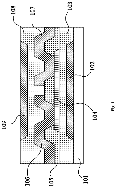
FIGS. 1, 2, and 3 are a side views of example transistor structures including example transistors with self aligned gates;
FIG. 4 is a flow diagram illustrating an example process for forming a transistor having a self aligned gate;
FIGS. 5A, 5B, 5C, 5D, 5E, 5F, 5G, 5H, 5I, 5J, and 5K are side views of example transistor structures as particular fabrication operations are performed;
FIG. 6 is an illustrative diagram of a mobile computing platform employing an integrated circuit with transistor(s) having self aligned gates; and
FIG. 7 is a functional block diagram of a computing device, all arranged in accordance with at least some implementations of the present disclosure.
Detailed description
One or more embodiments or implementations are now described with reference to the enclosed figures. While specific configurations and arrangements are discussed, it should be understood that this is done for illustrative purposes only. Persons skilled in the relevant art will recognize that other configurations and arrangements may be employed without departing from the spirit and scope of the description. It will be apparent to those skilled in the relevant art that techniques and/or arrangements described herein may also be employed in a variety of other systems and applications other than what is described herein.
Reference is made in the following detailed description to the accompanying drawings, which form a part hereof, wherein like numerals may designate like parts throughout to indicate corresponding or analogous elements. It will be appreciated that for simplicity and/or clarity of illustration, elements illustrated in the figures have not necessarily been drawn to scale. For example, the dimensions of some of the elements may be exaggerated relative to other elements for clarity. Further, it is to be understood that other embodiments may be utilized and structural and/or logical changes may be made without departing from the scope of claimed subject matter. It should also be noted that directions and references, for example, up, down, top, bottom, over, under, and so on, may be used to facilitate the discussion of the drawings and embodiments and are not intended to restrict the application of claimed subject matter. Therefore, the following detailed description is not to be taken in a limiting sense and the scope of claimed subject matter defined by the appended claims and their equivalents.
In the following description, numerous details are set forth. However, it will be apparent to one skilled in the art, that the present invention may be practiced without these specific details. In some instances, well-known methods and devices are shown in block diagram form, rather than in detail, to avoid obscuring the present invention. Reference throughout this specification to “an embodiment” or “one embodiment” means that a particular feature, structure, function, or characteristic described in connection with the embodiment is included in at least one embodiment of the invention. Thus, the appearances of the phrase “in an embodiment” or “in one embodiment” in various places throughout this specification are not necessarily referring to the same embodiment of the invention. Furthermore, the particular features, structures, functions, or characteristics may be combined in any suitable manner in one or more embodiments. For example, a first embodiment may be combined with a second embodiment anywhere the particular features, structures, functions, or characteristics associated with the two embodiments are not mutually exclusive.
As used in the description of the invention and the appended claims, the singular forms “a”, “an” and “the” are intended to include the plural forms as well, unless the context clearly indicates otherwise. It will also be understood that the term “and/or” as used herein refers to and encompasses any and all possible combinations of one or more of the associated listed items.
The terms “coupled” and “connected,” along with their derivatives, may be used herein to describe structural relationships between components. It should be understood that these terms are not intended as synonyms for each other. Rather, in particular embodiments, “connected” may be used to indicate that two or more elements are in direct physical or electrical contact with each other. “Coupled” my be used to indicated that two or more elements are in either direct or indirect (with other intervening elements between them) physical or electrical contact with each other, and/or that the two or more elements co-operate or interact with each other (e.g., as in a cause an effect relationship).
The terms “over,” “under,” “between,” “on”, and/or the like, as used herein refer to a relative position of one material layer or component with respect to other layers or components. For example, one layer disposed over or under another layer may be directly in contact with the other layer or may have one or more intervening layers. Moreover, one layer disposed between two layers may be directly in contact with the two layers or may have one or more intervening layers. In contrast, a first layer “on” a second layer is in direct contact with that second layer. Similarly, unless explicitly stated otherwise, one feature disposed between two features may be in direct contact with the adjacent features or may have one or more intervening features.
As used in throughout this description, and in the claims, a list of items joined by the term “at least one of” or “one or more of” can mean any combination of the listed terms. For example, the phrase “at least one of A, B or C” can mean A; B; C; A and B; A and C; B and C; or A, B and C.
Transistors, devices, apparatuses, computing platforms, and methods are described below related to transistors having self aligned gates.
As described above, it may be advantageous to reduce gate misalignments that may cause mistargeted device breakdown voltage or device failure. In one embodiment as described herein, a gallium nitride (GaN) transistor may include a self-aligned gate. For example, the self-aligned gate may be aligned to an opening of a spacer structure including lateral epitaxy overgrowths having the opening therebetween. The lateral epitaxy overgrowths may be formed over a raised source and a raised drain such that they extend toward each other but, as discussed, have an opening therebetween. In some examples, the lateral epitaxy overgrowths may be formed over a sacrificial patterned hardmask. The opening between the lateral epitaxy overgrowths may be used to align an optional gate recess in a polarization layer between the raised source and raised drain and/or to align the gate. As is discussed further herein, the polarization layer may be disposed over a device layer and may cause a 2D electron gas in the device layer as a transport channel. The gate or at least a portion of the gate adjacent to the polarization layer may be aligned to the opening and, in some examples, the gate or at least the portion of the gate may have a width not greater than a width of the opening.
In some examples, the gate may be formed such that a top of the gate is below the top surfaces of the lateral epitaxy overgrowths and such that gaps are formed between the gate and the lateral epitaxy overgrowths. Such a gap may reduce or eliminate parasitic gate leakage (e.g., leakage from the gate to the source or drain). In other examples, the gate may be formed such that a top of the gate extends above (e.g., vertically) and over (e.g., laterally) the tops of the lateral epitaxy overgrowths. In such examples, the material of the lateral epitaxy overgrowths may provide for reduced or eliminated parasitic gate leakage. For example, the material of the lateral epitaxy overgrowth, whether or not gaps are provided, may include a wide band gap semiconductor material such as gallium nitride or aluminum gallium nitride or the like. Such materials may reduce or eliminate parasitic gate leakage for example. As used herein, a semiconductor material may be any material having an electrical conductivity between that of a conductor and that of an insulator and a wide band gap material may be any material having a band gap that is wide as compared to silicon (˜1.1 eV). For example, wide band gap materials may have a band gap greater than 2 eV. Such elimination of parasitic gate leakage may provide for high voltage operation of the transistors discussed herein. Furthermore, in some examples, a gate dielectric may be disposed between the polarization layer and the portion of the gate adjacent to the polarization layer. In some examples, the gate dielectric may extend over the polarization layer and the lateral epitaxial overgrowths or portions thereof. These embodiments are discussed further herein with respect to FIGS. 1, 2, and 3 .
FIG. 1 is a cross-sectional (side) view of an example transistor structure 150 including an example transistor 100 , arranged in accordance with at least some implementations of the present disclosure. As shown in FIG. 1 , transistor structure 150 may include a device layer 101 , a polarization layer 104 having a gate recess 117 , a gate dielectric 105 , a raised source 102 , a raised drain 103 , a gate 106 , a lateral epitaxy overgrowth 107 and a lateral epitaxy overgrowth 109 . As shown, an opening 111 may be provided between a portion 108 of lateral epitaxy overgrowth 107 , and a portion 110 of lateral epitaxy overgrowth 109 . In some examples, opening 111 may be between portions of gate dielectric 105 covering portions 108 , 109 of lateral epitaxy overgrowths 107 , 109 as shown. In other examples, gate dielectric may not cover portions 108 , 109 of lateral epitaxy overgrowths 107 , 109 as illustrated with respect to FIG. 2 . In some examples, gate recess 117 and/or gate 106 may be aligned with opening 111 . As used herein, the term aligned is used to indicate the described elements are substantially arranged along a line (e.g., typically a vertical line). For example, the vertical direction as used herein may be in the z-direction as shown in FIGS. 1-3 . For example, gate recess 117 and opening 111 may be aligned such that they are substantially aligned along centerline, C.sub.L, as shown in FIG. 1 . In some examples, the described elements may have further characteristics beyond being aligned. For example, a width of gate recess 117 and a width of opening 111 may be substantially the same or gate recess 117 may have a width that is not more than the width of opening 111 or the like. However, such geometries are not needed for elements to be aligned as discussed herein.
Continuing with FIG. 1 , as shown, transistor structure 150 may include device layer 101 . Device layer 101 may include, for example, a III-N material such as an epitaxial III-N material. Device layer 101 may include any suitable material such as gallium nitride (GaN) and device layer 101 may be formed on any suitable substrate (not shown). Furthermore, transistor structure 150 may include polarization layer 104 . Polarization layer 104 may include any material, materials, or material stack that may provide a 2D electron gas (not shown) in device layer 101 . For example, polarization layer 104 may be aluminum nitride (AlN), aluminum indium nitride (AlInN), or aluminum gallium nitride (AlGaN), or any combination thereof. For example, polarization layer 104 , due to the polarization difference between device layer 101 (e.g., the epitaxial III-N material of device layer 101 ) and polarization layer 104 , may provide for the formation of a high charge density and high mobility 2D electron gas in device layer 101 . In some examples, a channel (not shown) may be formed in device layer 101 substantially under gate 106 during the operation of transistor 100 .
As shown in FIG. 1 , polarization layer 104 may include a gate recess 117 . Gate recess 117 may be aligned with opening 111 . For example, gate recess 117 and opening 111 may be aligned along centerline C.sub.L as shown. For example, lateral epitaxy overgrowth 107 and lateral epitaxy overgrowth 109 may be symmetrical or substantially symmetrical with respect to a centerline of gate 106 and/or a centerline of gate recess 117 . In some embodiments, lateral epitaxy overgrowth 107 and lateral epitaxy overgrowth 109 may provide a symmetric mask for the formation of gate 106 and/or gate recess 117 . Furthermore, gate recess 117 may have a width or length, L.sub.G, that is substantially the same as the width of opening 111 (e.g., the opening between portions 108 , 110 of lateral epitaxy overgrowths 107 , 109 ). In some examples, gate recess 117 may have a width that is not greater than a width of opening 111 . In some examples, length L.sub.G may define a gate length of transistor 100 . Gate recess 117 may have substantially any depth within polarization layer 104 . For example, gate recess 117 may have a depth of approximately half of the depth of polarization layer 104 or the like. In some examples, gate recess 117 (e.g., the depth of gate recess 117 ) may be used to tune a threshold voltage, V.sub.T, of transistor 100 . Furthermore, transistor 100 may include gate dielectric 105 . Gate dielectric 105 may include any suitable material or materials such as a high-k dielectric material. For example, gate dielectric 105 may include a high-k dielectric material and gate 106 may be a metal gate such that transistor 100 may be characterized as a high-k metal gate transistor. In some examples, as discussed with respect to FIG. 2 , no gate recess and/or no gate dielectric material may be implemented. For example, transistors that include gate dielectric 105 may be characterized as field effect transistors (FETs) and transistors that do not include gate dielectric 105 may be characterized as high-electron-mobility transistors (HEMTs).
Also as shown in FIG. 1 , transistor 100 may include raised source 102 and raised drain 103 . As shown, raised source 102 and raised drain 103 may be disposed within trenches of device layer 101 . Also as shown, raised source 102 and raised drain 103 may be disposed such that polarization layer 104 is between raised source 102 and raised drain 103 . Raised source 102 and raised drain 103 may include any suitable material or materials that may provide a current source and current drain for transistor 100 and that may provide for epitaxial growth of lateral epitaxy overgrowth 107 , 109 . In some examples, raised source 102 and raised drain 103 may include an epitaxial material or material. In some examples, source 102 and raised drain 103 may include indium gallium nitride such as an N+ indium gallium nitride. Although illustrated herein with raised source 102 and raised drain 103 , in some examples, planar source and drain structures may be used.
Continuing with FIG. 1 , transistor structure 150 may include lateral epitaxy overgrowths 107 , 109 . As shown, lateral epitaxy overgrowth 107 may be disposed over raised source 102 and lateral epitaxy overgrowth 107 may have a portion 108 that extends laterally toward gate 106 . As used herein, the term laterally indicates a direction that is horizontal or substantially horizontal. For example, the horizontal direction as used herein may be in the x-direction as shown in FIGS. 1-3 . Similarly, lateral epitaxy overgrowth 109 may be disposed over raised drain 104 and lateral epitaxy overgrowth 109 may have a portion 110 that extends laterally toward gate 106 . As shown, lateral epitaxy overgrowth 107 and lateral epitaxy overgrowth 109 may have opening 111 between portions 108 and 110 . As discussed, gate recess 117 and/or gate 106 may be aligned with opening 111 .
For example, lateral epitaxy overgrowths 107 , 109 may provide for spacer structures for the alignment of gate recess 117 and/or gate 106 along a line or plane between the opening of the spacer structure. In some examples, such aligned gate recess 117 and/or gate 106 may be formed after the formation of lateral epitaxy overgrowths 107 , 109 . In such examples, transistor 100 may be characterized as a self-aligned gate last transistor such that gate 106 is self-aligned to lateral epitaxy overgrowths 107 , 109 and such that gate 106 is formed after lateral epitaxy overgrowths 107 , 109 . Lateral epitaxy overgrowths 107 , 109 may be any suitable material or materials that may provide for opening 111 and, in some examples, electrical isolation between gate 106 and raised source 102 and between gate 106 an raised drain 104 . In some embodiments, lateral epitaxy overgrowths 107 , 109 may include gallium nitride or aluminum gallium nitride or the like. In an embodiment, lateral epitaxy overgrowths 107 , 109 include undoped gallium nitride. In another embodiment, lateral epitaxy overgrowths 107 , 109 include undoped aluminum gallium nitride (Al.sub.xGa.sub.1-xN) such that the percentage of aluminum is about 10% (i.e., x=0.1) with a balance of gallium (e.g., Al.sub.0.1Ga.sub.0.9N). Gate 106 may have any suitable conductive material. As discussed, in some examples, gate 106 may include a metal as discussed herein.
As shown in FIG. 1 , in some examples, a top 112 of gate 106 may be below a top 113 of lateral epitaxy overgrowth 107 and a top 114 of lateral epitaxy overgrowth 109 . In some examples, top 112 of gate 106 may also be below bottom surfaces (not labeled) of portion 108 of lateral epitaxy overgrowth 107 and potion 110 of lateral epitaxy overgrowth 109 as shown. Furthermore, in some examples, a gap 115 may be provided between gate 106 and lateral epitaxy overgrowth 107 and a gap 116 may be provided between gate 106 and lateral epitaxy overgrowth 109 . In some examples, gaps 115 , 116 may be filled with an insulating dielectric such as silicon oxide (SiO.sub.2) or silicon nitride (SiN) or the like. In examples including gaps 115 , 116 , gaps 115 116 may provide isolation such that any parasitic gate leakage (e.g., leakage from gate 106 to raised source 102 or from gate 106 to raised drain 104 ) may be reduced or eliminated. In examples where gaps 115 , 116 are not provided (e.g., examples where portion 108 of lateral epitaxy overgrowth 107 and/or portion 110 of lateral epitaxy overgrowth 109 are in contact with gate 106 ), the material of lateral epitaxy overgrowths 107 , 109 may be chosen to reduce or eliminate such parasitic gate leakage. For example, as discussed, lateral epitaxy overgrowths 107 , 109 may include a wide band gap semiconductor material such as GaN or Al.sub.xGa.sub.1-xN to reduce or eliminate parasitic gate leakage. Furthermore, in some examples, as shown, gate dielectric 105 may provide a conformal insulating dielectric between gate 106 and lateral epitaxy overgrowths 107 , 109 . Such a gate dielectric may be deposited using any technique discussed herein with atomic layer deposition being particularly advantageous. Such a configuration of gate dielectric 105 may provide the needed isolation to prevent gate leakage and/or provide additional isolation.
FIG. 2 is a cross-sectional (side) view of an example transistor structure 250 including an example transistor 200 , arranged in accordance with at least some implementations of the present disclosure. As shown in FIG. 2 , transistor structure 250 may include device layer 101 , polarization layer 104 , raised source 102 , raised drain 103 , gate 106 , lateral epitaxy overgrowth 107 , and lateral epitaxy overgrowth 109 . Furthermore, opening 111 may be provided between portion 108 of lateral epitaxy overgrowth 107 and portion 110 of lateral epitaxy overgrowth 109 as discussed with respect to FIG. 1 herein. As discussed, gate 106 may be may be aligned with opening 111 .
In the example of FIG. 2 , transistor 200 may not include a gate dielectric. In such examples, transistor 200 may be characterized as high-electron-mobility transistor (HEMT). Such HEMTs may offer advantages such as excellent performance at high voltage and high frequencies. Also as shown in FIG. 2 , transistor 200 may not include a gate recess. Such exclusion of a gate recess may offer simplicity in fabrication for example. Although transistors are illustrated with a gate recess and gate dielectric (e.g., in FIG. 1 ) and without a gate recess and without a gate dielectric (e.g., in FIG. 2 ), other combinations are available. For example, transistors may be formed with a gate dielectric but without a gate recess or with a gate recess but without a gate dielectric. Furthermore, the illustrated elements of transistor structure 250 such as device layer 101 , polarization layer 104 , raised source 102 , raised drain 103 , gate 106 , lateral epitaxy overgrowth 107 , and lateral epitaxy overgrowth 109 may include any materials or other characteristics as discussed with respect to transistor structure 150 and such details will not be repeated for the sake of brevity and clarity of presentation.
FIG. 3 is a cross-sectional (side) view of an example transistor structure 350 including an example transistor 300 , arranged in accordance with at least some implementations of the present disclosure. As shown in FIG. 1 , transistor structure 150 may include device layer 101 , polarization layer 104 having gate recess 117 , gate dielectric 105 , raised source 102 , raised drain 103 , a gate 306 , lateral epitaxy overgrowth 107 and lateral epitaxy overgrowth 109 . As shown, opening 111 may be provided between a portion 108 of lateral epitaxy overgrowth 107 , and a portion 110 of lateral epitaxy overgrowth 109 . In some examples, gate recess 117 and/or gate 306 may be aligned with opening 111 .
As shown, in the example of FIG. 3 , transistor 300 may include gate 306 such that gate 306 has a portion 307 that extends above (e.g., vertically above) top 113 of lateral epitaxy overgrowth 107 and above top 114 of lateral epitaxy overgrowth 109 . Furthermore, as shown, portion 307 may extend over (e.g., laterally over) portion 108 of lateral epitaxy overgrowth 107 or at least part of portion 108 and over portion 110 of lateral epitaxy overgrowth 109 or at least part of portion 110 . As shown, gate 306 may have a top 308 that extends above top 113 of lateral epitaxy overgrowth 107 and above top 114 of lateral epitaxy overgrowth 109 . As shown, gate 306 transistor structure 350 may have a substantially T-shape in cross section. As discussed with respect to gate 106 , gate 306 may be aligned with opening 111 . In particular, a portion 309 of gate 306 may be self aligned via opening 111 as discussed. For example, portion 309 of gate 306 may be aligned with opening 111 . In some examples, portion 307 of gate 306 may be formed via patterning a bulk material deposition or via a lift off technique as is discussed further herein with respect to FIG. 5K . In such examples, portion 307 of gate 306 may be patterned and therefore not self aligned to opening 111 . However, portion 309 of gate 306 may be self aligned to opening 111 via the constraints applied by lateral epitaxy overgrowths 107 , 109 .
Additional details associated with the described features of transistor structures 150 , 250 , 350 and/or transistors 100 , 200 , 300 are provided herein with respect to FIGS. 5A-5K , which discuss the formation of transistor structures 150 , 250 , 350 and/or transistors 100 , 200 , 300 as well as the formation of transistor structure 523 and transistor 524 as is discussed with respect to FIG. 5J .
Furthermore, transistor structures 150 , 250 , 350 , 523 and/or transistors 100 , 200 , 300 , 524 may be implemented in an electronic device structure comprising a system on a chip. For example, the structure may include a silicon Complementary Metal Oxide Semiconductor (CMOS) circuit portion, a III-N material based device portion, and/or other device portions, implemented on a substrate. The III-N material based devices (e.g., any, some or all of transistors 100 , 200 , 300 , 524 ) may be formed on III-N material regions that are formed on, over, or within the substrate. For example, the substrate may be silicon as discussed herein. The III-N material regions may be formed adjacent to CMOS circuit portions based on device requirements for example.
Although illustrated with respect to structures having lateral and/or planar channels, the techniques discussed herein may be extended to vertically oriented MOSFET devices, tunnel field effect transistors (TFET), or the like. Such implementations may have the advantage of additional channel capacity using similar device geometries for example.
FIG. 4 is a flow diagram illustrating an exemplary process 400 for forming a transistor having a self aligned gate, arranged in accordance with at least some implementations of the present disclosure. For example, process 400 may be implemented to fabricate any of transistors 100 , 200 , 300 , 524 as discussed herein. In the illustrated implementation, process 400 may include one or more operations as illustrated by operations 401 - 404 . However, embodiments herein may include additional operations, certain operations being omitted, or operations being performed out of the order provided.
Process 400 may begin at operation 401 , “Dispose a Polarization Layer over a Device Layer”, where a polarization layer may be disposed over a device layer. In an embodiment, polarization layer 104 may be formed over device layer 101 as is discussed further with respect to FIG. 5A and elsewhere herein. In an embodiment, polarization layer 104 may include aluminum indium nitride and device layer 101 may include gallium nitride.
Process 400 may continue at operation 402 , “Form a Source and a Drain such that the Polarization Layer is between the Source and Drain”, where a source and a drain may be formed such that the polarization layer is between the source and drain. In an embodiment, a raised source such as raised source 102 and a raised drain such as raised drain 104 may be formed with trenches of device layer 101 as is discussed further herein with respect to FIGS. 5B-5E and elsewhere herein. In an embodiment, raised source 102 and raised drain 104 may include N+ indium gallium nitride.
Process 400 may continue at operation 403 , “Form Lateral Epitaxy Overgrowths having an Opening therebetween over the Source and Drain”, where lateral epitaxy overgrowths may be formed over the source and the drain. For example, a first lateral epitaxy overgrowth may be formed over the raised source and a second lateral epitaxy overgrowth may be formed over the raised drain such that the first and second lateral epitaxy overgrowths have an opening between a laterally extending first portion of the first lateral epitaxy overgrowth and laterally extending second portion of the second lateral epitaxy overgrowth as is discussed further herein with respect to FIGS. 5F-5H and elsewhere herein. In an embodiment, lateral epitaxy overgrowth 107 may be formed over raised source 102 and lateral epitaxy overgrowth 109 may be formed over raised source 104 such that opening 111 is provided between portion 108 of lateral epitaxy overgrowth 107 and portion 110 of lateral epitaxy overgrowth 109 . In an embodiment, lateral epitaxy overgrowths 107 , 109 may include undoped gallium nitride.
Process 400 may continue at operation 404 , “Dispose a Self Aligned Gate between the Source and Drain and over the Polarization Layer”, where a self aligned gate may be disposed between the source and drain and over the polarization layer. In an embodiment, gate 106 may be disposed between raised source 102 and raised drain 104 and over polarization layer 104 as is discussed further with respect to FIG. 5J and elsewhere herein. In an embodiment, gate 306 may be disposed between raised source 102 and raised drain 104 and over polarization layer 104 as is discussed further with respect to FIG. 5K and elsewhere herein. In some examples, at least a portion of the gate may be aligned with opening 111 (e.g., a centerline of the gate may be aligned with a centerline of opening 111 ). In an embodiment, gate 106 may be aligned with opening 111 . In another embodiment, portion 309 of gate 306 may be aligned with opening 311 .
As discussed, process 400 may be implanted to fabricate any of transistors 100 , 200 , 300 , 524 . Further details associated with such fabrication techniques are discussed herein an in particular, with respect to FIGS. 5A-5K . Any one or more of the operations of process 400 (or the operations discussed herein with respect to FIGS. 5A-5K ) may be undertaken in response to instructions provided by one or more computer program products. Such program products may include signal bearing media providing instructions that, when executed by, for example, a processor, may provide the functionality described herein. The computer program products may be provided in any form of computer readable medium. Thus, for example, a processor including one or more processor core(s) may undertake one or more of the described operations in response to instructions conveyed to the processor by a computer readable medium.
FIGS. 5A-5K are side views of example transistor structures as particular fabrication operations are performed, arranged in accordance with at least some implementations of the present disclosure. As shown in FIG. 5A , transistor structure 500 includes polarization layer 104 formed over a device layer 101 . In some examples, device layer 101 may be disposed over a substrate (not shown). For example, the substrate may be a substrate substantially aligned along a predetermined crystal orientation (e.g., (100), (111), (110), or the like). In some examples, the substrate may include a semiconductor material such as monocrystalline silicon (Si), germanium (Ge), silicon germanium (SiGe), a III-V materials based material (e.g., gallium arsenide (GaAs)), a silicon carbide (SiC), a sapphire (Al.sub.2O.sub.3), or any combination thereof. In some examples, substrate 101 may include silicon having a
crystal orientation with a 4°-11° miscut (with 4°-6° being particularly advantageous). Examples using a silicon substrate having a crystal orientation of
may offer the advantage of having a smaller mismatch for subsequent epitaxial growth. In various examples, the substrate may include metallization interconnect layers for integrated circuits or electronic devices such as transistors, memories, capacitors, resistors, optoelectronic devices, switches, or any other active or passive electronic devices separated by an electrically insulating layer, for example, an interlayer dielectric, a trench insulation layer, or the like.
Device layer 101 may be formed using any suitable technique or techniques. For example, device layer 101 may be formed using any suitable epitaxial growth technique such as an epitaxial growth via chemical vapor deposition (CVD), metal organic chemical vapor deposition (MOCVD), atomic layer deposition (ALD), or any other epitaxial growth technique, with MOCVD being particularly advantageous. In some examples, the formation of device layer 101 may include defect trapping techniques. In some embodiments, devices may be formed in a defect free region of device layer 101 such as an island of material or the like. Furthermore, device layer 101 may include any suitable III-N material such as, for example, an epitaxial III-N material. In an embodiment, device layer 101 is gallium nitride. Device layer 101 may be any suitable thickness such as, for example, 100-500 nm or more.
Also as shown in FIG. 5A , polarization layer 104 may be formed over device layer 101 . Polarization layer 104 may be formed using any suitable technique or techniques. In some examples, polarization layer 104 may be performed via an epitaxial growth technique such as an epitaxial growth via chemical vapor deposition, metal organic chemical vapor deposition, atomic layer deposition, or the like. Polarization layer 104 may include any material or material stacks that may provide a 2D electron gas in device layer 101 . For example, polarization layer 104 may be aluminum nitride (AlN), aluminum indium nitride (AlInN), or aluminum gallium nitride (AlGaN), or any combination thereof. Polarization layer 104 may have any suitable thickness. In some examples, polarization layer 104 may have a thickness of 6 to 10 nm.
FIG. 5B illustrates a transistor structure 501 similar to transistor structure 500 , after the formation of hardmask stack 505 and the formation of patterned layer 506 . As shown, in some examples, hardmask stack 505 may include three layers including hardmask layer 502 , hardmask layer 503 , and hardmask layer 504 . However, any number of hardmask layers may be used such as one, two, three, four, or more. Furthermore, hardmask stack 505 may include any suitable material or materials that will provide a mask for the subsequent formation of trenches or recesses in polarization layer 104 and device layer 101 and may be selective to the subsequently formed raised source 102 and raised drain 104 (e.g., epitaxial III-N materials) such as, for example, silicon oxide, silicon nitride, silicon oxynitride, aluminum oxide, or the like. In an embodiment, hardmask layer 502 is aluminum oxide (Al.sub.2O.sub.3), hardmask layer 503 is silicon nitride (SiN), and hardmask layer 504 is aluminum oxide. The layers of hardmask stack 505 may be formed using any suitable technique or techniques. For examples, hardmask layers 502 - 504 or the like may be deposited using a blanket deposition techniques such as chemical vapor deposition, plasma enhanced chemical vapor deposition, physical vapor deposition, molecular beam epitaxy, metalorganic chemical vapor deposition, atomic layer deposition, or the like.
Hardmask stack 505 may have any suitable thickness. In some examples, a thickness of hardmask stack 505 may be provided such that subsequent processing such as etch processing may reduce the size of hardmask stack 505 to a desired height for subsequent processing. For example, as is discussed further below, a patterned and post-etch hardmask may be used as a sacrificial layer for the formation of lateral epitaxy overgrowths 107 , 109 . In such examples, the thickness of hardmask stack 505 may be provided such that a thickness of the patterned and post-etch hardmask may be of a desired thickness for the formation of lateral epitaxy overgrowths 107 , 109 . In some examples, hardmask stack 505 may have a thickness of about 120 to 200 nm. In an embodiment, hardmask layer 502 has a thickness of about 10 nm, hardmask layer 503 has a thickness of about 120 nm, and hardmask layer 504 has a thickness of about 10 nm.
Patterned layer 506 may include any suitable material for patterning hardmask stack 505 such as a resist and patterned layer 506 may be formed using any suitable techniques such as photolithography techniques.
FIG. 5C illustrates a transistor structure 507 similar to transistor structure 501 , after the patterning of hardmask stack 505 to form a patterned hardmask stack 508 . As shown in FIG. 5C , in some examples, patterned hardmask stack 508 may have tapered sidewalls 509 . Hardmask stack 505 may be patterned using any suitable technique or techniques to form patterned hardmask stack 508 . In some examples, hardmask stack 508 patterned using etch processing. Patterned hardmask stack 508 may have any suitable width, W.sub.HM, such as a width in the range of 120 to 300 nm.
The description continues in the full USPTO document.
 Lapsed, fee not paid4 drawings