Incorporation by reference
The present application claims priority under 35 U.S.C. §119 to Japanese Patent Application No. 2016-007081, filed on Jan. 18, 2016. The contents of this application are incorporated herein by reference in their entirety.
Background
The present disclosure relates to an image forming apparatus.
It is known that a value of a current flowing through a transfer roller in an image forming apparatus is measured.
For example, a generally known image forming apparatus determines a resistance value of a transfer roller from a value of a current detected by a detection circuit. This image forming apparatus includes the detection circuit, a constant voltage circuit and a controller. The detection circuit detects a value of a current flowing through the transfer roller. The constant voltage circuit performs constant voltage control of a voltage that is applied to the transfer roller. Further, the resistance value of the transfer roller is determined from the value of the current detected by the detection circuit when the constant voltage control is performed. The controller controls a transfer voltage based on the determined resistance value.
Through the above image forming apparatus, an appropriate transfer voltage can be applied.
Summary
An image forming apparatus of the present disclosure forms an image on a recording medium. The image forming apparatus includes a specified number of developing devices, the specified number of primary transfer rollers, an intermediate transfer belt, voltage applicators, a current detector, and a voltage controller. The specified number is two or more. The specified number of developing devices each form a toner image on a corresponding one of the specified number of photosensitive drums. The specified number of primary transfer rollers are each located opposite to a corresponding one of the specified number of photosensitive drums. The intermediate transfer belt is held between the specified number of photosensitive drums and the specified number of primary transfer rollers. The voltage applicators each apply a voltage to a corresponding one of the specified number of primary transfer rollers. The current detector detects a total current value that is a sum of values of currents flowing through the specified number of primary transfer rollers. The voltage controller controls voltage values of voltages that the voltage applicators apply to the specified number of primary transfer rollers. The voltage controller causes a detection voltage to be applied to one primary transfer roller of the specified number of primary transfer rollers while causing a voltage having the same polarity as the detection voltage to be applied to all other of the primary transfer rollers. The detection voltage is a voltage that is applied to detect a resistance value of the one primary transfer roller and that has a predetermined voltage value.
Brief description of the drawings
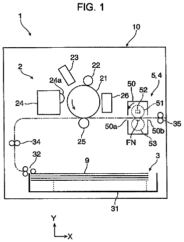
FIG. 1 is a side view illustrating a configuration of an image forming apparatus according to an embodiment of the present disclosure.
FIG. 2 is a side view illustrating configurations of an image forming unit and a transfer section illustrated in FIG. 1 .
FIG. 3 is a side view illustrating a configuration of a power supply section illustrated in FIG. 1 .
FIG. 4 is a diagram illustrating a configuration of a controller illustrated in FIG. 1 .
FIGS. 5A to 5D are graphs showing an example of operation of a voltage controller when the voltage value of a second voltage VL 2 is the same as the voltage value of a first voltage VL 1 . FIG. 5A is a graph showing variation of an applied voltage applied to a primary transfer roller for Y color. FIG. 5B is a graph showing variation of an applied voltage applied to a primary transfer roller for C color. FIG. 5C is a graph showing variation of an applied voltage applied to a primary transfer roller for M color. FIG. 5D is a graph showing variation of an applied voltage applied to a primary transfer roller for K color.
FIG. 6 is a graph showing a relationship between voltage values of a voltage applied by a voltage applicator illustrated in FIG. 3 and current values detected by a current detector.
FIG. 7 is a flowchart illustrating operation of the controller illustrated in FIG. 4 .
FIG. 8 is a flowchart illustrating the operation of the controller illustrated in FIG. 4 .
FIGS. 9A to 9D are graphs showing an example of operation of the voltage controller when the voltage value of the second voltage VL 2 is greater than the voltage value of the first voltage VL 1 . FIG. 9A is a graph showing variation of an applied voltage applied to the primary transfer roller for Y color. FIG. 9B is a graph showing variation of an applied voltage applied to the primary transfer roller for C color. FIG. 9C is a graph showing variation of an applied voltage applied to the primary transfer roller for M color. FIG. 9D is a graph showing variation of an applied voltage applied to the primary transfer roller for K color.
Detailed description
The following describes an embodiment of the present disclosure with reference to the drawings ( FIGS. 1 to 9D ). Elements that are the same or substantially equivalent are indicated by the same reference signs in the drawings and explanation thereof is not repeated.
First, an image forming apparatus 1 according to the present embodiment will be described with reference to FIG. 1 . FIG. 1 is a diagram illustrating a configuration of the image forming apparatus 1 according to the present embodiment. The image forming apparatus 1 according to the present embodiment is a color copier.
The image forming apparatus 1 forms an image on paper P. The image forming apparatus 1 includes a housing 10 , a paper feed section 2 , a conveyance section L, a toner replenishment unit 3 , an image forming unit 4 , a transfer section 5 , a power supply section 6 , a fixing section 7 , an ejection section 8 , and a controller 9 . The paper P corresponds to an example of what is referred to as “a recording medium”.
The paper feed section 2 is disposed in a lower location of the housing 10 and feeds the paper P to the conveyance section L. The paper feed section 2 can accommodate a plurality of sheets of the paper P. The paper feed section 2 feeds the paper P to the conveyance section L one uppermost sheet of the paper P at a time.
The conveyance section L conveys the paper P fed by the paper feed section 2 to the ejection section 8 through the transfer section 5 and the fixing section 7 .
The toner replenishment unit 3 includes four toner cartridges 3 y , 3 c , 3 m , and 3 k which are containers for supplying toners to the image forming unit 4 . The toner cartridge 3 y contains a yellow toner. The toner cartridge 3 c contains a cyan toner. The toner cartridge 3 m contains a magenta toner. The toner cartridge 3 k contains a black toner.
The image forming unit 4 includes four image forming sections 4 y , 4 c , 4 m , and 4 k . The yellow toner is supplied from the toner cartridge 3 y to the image forming section 4 y . The cyan toner is supplied from the toner cartridge 3 c to the image forming section 4 c . The magenta toner is supplied from the toner cartridge 3 m to the image forming section 4 m . The black toner is supplied from the toner cartridge 3 k to the image forming section 4 k . A configuration of the image forming unit 4 will be described further below with reference to FIG. 2 .
The transfer section 5 includes an intermediate transfer belt 54 . The image forming unit 4 forms toner images on the intermediate transfer belt 54 , and the transfer section 5 transfers the toner images onto the paper P. A configuration of the transfer section 5 will be described further below with reference to FIG. 2 .
The power supply section 6 applies transfer voltages to the transfer section 5 . The power supply section 6 also detects values of transfer currents flowing through the transfer section 5 . A configuration of the power supply section 6 will be described further below with reference to FIG. 3 .
The fixing section 7 includes a heating roller 71 and a pressure roller 72 as a pair of rollers for fixing the toner images transferred onto the paper P by the transfer section 5 . The heating roller 71 and the pressure roller 72 apply heat and pressure respectively to the paper P. Through the above, the fixing section 7 fixes the unfixed toner images transferred onto the paper P by the transfer section 5 . The ejection section 8 ejects the paper P having the toner images fixed thereon out of the apparatus.
The controller 9 controls operation of the image forming apparatus 1 . A configuration of the controller 9 will be described further below with reference to FIG. 4 .
Next, the configurations of the image forming unit 4 and the transfer section 5 will be described with reference to FIG. 2 . FIG. 2 is a side view illustrating the configurations of the image forming unit 4 and the transfer section 5 . As illustrated in FIG. 2 , the image forming unit 4 includes the four image forming sections 4 y , 4 c , 4 m , and 4 k . A “specified number” is four in the present embodiment.
The image forming sections 4 y , 4 c , 4 m , and 4 k each include a light exposure device 41 , a photosensitive drum 42 , a developing device 43 , a charging roller 44 , and a cleaning blade 45 . The four image forming sections 4 y , 4 c , 4 m , and 4 k have substantially the same configuration except the colors of the toners to be supplied thereto. The present specification therefore describes the configuration of the image forming section 4 y to which the yellow toner is supplied, and omits description of the configurations of the image forming sections other than the image forming section 4 y , that is, image forming sections 4 c , 4 m , and 4 k.
The image forming section 4 y has a light exposure section 41 y ( 41 ), a photosensitive drum 42 y ( 42 ), a developing device 43 y ( 43 ), a charging roller 44 y ( 44 ), and a cleaning blade 45 y ( 45 ).
The charging roller 44 y charges the photosensitive drum 42 y to a specific potential. The light exposure section 41 y irradiates the photosensitive drum 42 y with laser light to form an electrostatic latent image on the photosensitive drum 42 y . The developing device 43 y includes a development roller 431 y . The development roller 431 y supplies the yellow toner to the photosensitive drum 42 y and develops the electrostatic latent image to form a toner image. As a result, the toner image in yellow is formed on a circumferential surface of the photosensitive drum 42 y.
An edge of the cleaning blade 45 y (the top edge in FIG. 2 ) is in sliding contact with the circumferential surface of the photosensitive drum 42 y . The edge of the cleaning blade 45 y in sliding contact with the circumferential surface of the photosensitive drum 42 y removes the yellow toner remaining on the circumferential surface of the photosensitive drum 42 y.
The transfer section 5 transfers toner images onto the paper P. The transfer section 5 includes four primary transfer rollers 51 ( 51 y , 51 c , 51 m , and 51 k ), a secondary transfer roller 52 , a drive roller 53 , the intermediate transfer belt 54 , a driven roller 55 , and a blade 56 .
The transfer section 5 transfers onto the intermediate transfer belt 54 toner images respectively formed on the photosensitive drums 42 ( 42 y , 42 c , 42 m , and 42 k ) of the image forming sections 4 y , 4 c , 4 m , and 4 k such that the toner images are superimposed on one another. The transfer section 5 further transfers the superimposed toner images from the intermediate transfer belt 54 to the paper P.
The primary transfer roller 51 y is disposed opposite to the photosensitive drum 42 y with the intermediate transfer belt 54 therebetween. The primary transfer roller 51 y can come in or out of press contact with the photosensitive drum 42 y with the intermediate transfer belt 54 therebetween through driving by a driving mechanism, not illustrated. The primary transfer roller 51 y is normally in press contact with the photosensitive drum 42 y with the intermediate transfer belt 54 therebetween. Like the primary transfer roller 51 y , the other primary transfer rollers 51 c , 51 m , and 51 k are each in press contact with a corresponding one of the photosensitive drums 42 ( 42 c , 42 m , or 42 k ), with the intermediate transfer belt 54 therebetween.
The drive roller 53 is disposed opposite to the secondary transfer roller 52 and drives the intermediate transfer belt 54 .
The intermediate transfer belt 54 is an endless belt that is stretched around the four primary transfer rollers 51 , the drive roller 53 , and the driven roller 55 . The intermediate transfer belt 54 is driven by the drive roller 53 to circulate in a counterclockwise direction as indicated by arrows F 1 and F 2 in FIG. 2 . An outer surface of the intermediate transfer belt 54 is in contact with circumferential surfaces of the respective photosensitive drums 42 ( 42 y , 42 c , 42 m , and 42 k ). Toner images are transferred by the primary transfer rollers 51 ( 51 y , 51 c , 51 m , and 51 k ) from the photosensitive drums 42 ( 42 y , 42 c , 42 m , and 42 k ) to the outer surface of the intermediate transfer belt 54 .
The driven roller 55 is driven to rotate by circulation of the intermediate transfer belt 54 . The blade 56 is disposed opposite to the driven roller 55 with the intermediate transfer belt 54 therebetween. The blade 56 removes toners remaining on the outer surface of the intermediate transfer belt 54 .
The secondary transfer roller 52 is pressed against the drive roller 53 . As a result, the secondary transfer roller 52 and the drive roller 53 form a nip N therebetween. The secondary transfer roller 52 and the drive roller 53 transfer the toner images from the intermediate transfer belt 54 to the paper P while the paper P is passing through the nip N.
Next, the power supply section 6 will be described with reference to FIG. 3 . FIG. 3 is a side view illustrating the configuration of the power supply section 6 . The power supply section 6 includes voltage applicators 61 and a current detector 62 . The voltage applicators 61 apply voltages to the primary transfer rollers 51 .
The voltage applicators 61 include four voltage applicators 61 y , 61 c , 61 m , and 61 k . The four voltage applicators 61 y , 61 c , 61 m , and 61 k apply voltages to the primary transfer rollers 51 y , 51 c , 51 m , and 51 k , respectively. For example, the voltage applicator 61 y applies to the primary transfer roller 51 y a voltage of opposite polarity (a negative voltage in the present embodiment) to charging polarity of the toner. The photosensitive drums 42 ( 42 y , 42 c , 42 m , and 42 k ) are grounded. As a result, the voltage applicator 61 y applies a voltage between the primary transfer roller 51 y and the photosensitive drum 42 y.
The current detector 62 detects a total current value JS that is a sum of values of currents flowing through the respective four primary transfer rollers 51 y , 51 c , 51 m , and 51 k.
Next, the configuration of the controller 9 will be described with reference to FIG. 4 . FIG. 4 is a diagram illustrating the configuration of the controller 9 . The controller 9 includes a central processing unit (CPU) and a memory. A control program is stored in the memory. The CPU implements various functional sections through execution of the control program. Also, the CPU causes the memory to implement various functional sections through execution of the control program. As a result, the various functional sections implemented by the controller 9 control operation of the image forming apparatus 1 . The controller 9 includes a voltage controller 911 , a current acquiring section 912 , a resistance calculator 913 , an adjuster 914 , and a voltage and current storage section 92 .
The voltage and current storage section 92 stores therein voltage values VT of voltages that the voltage applicators 61 apply to the primary transfer rollers 51 in association with total current values JS detected by the current detector 62 . The voltage values VT of the voltages and the total current values JS stored in the voltage and current storage section 92 are read by the resistance calculator 913 and the adjuster 914 .
The voltage controller 911 controls the voltages that the voltage applicators 61 apply to the primary transfer rollers 51 y , 51 c , 51 m , and 51 k . More specifically, the voltage controller 911 causes a detection voltage VS to be applied to one primary transfer roller 51 of the four primary transfer rollers 51 while causing a first voltage VL 1 having the same polarity as the detection voltage VS to be applied to all the other primary transfer rollers 51 . The one primary transfer roller 51 is for example the primary transfer roller 51 y , and all the other primary transfer rollers 51 are for example the primary transfer rollers 51 c , 51 m , and 51 k . The detection voltage VS is a voltage that is applied to detect a resistance value R between the one primary transfer roller 51 and a corresponding one of the photosensitive drums 42 . The detection voltage VS has a predetermined voltage value (for example, 1000 V). The first voltage VL 1 has a voltage value of at least one-200th and no greater than one-tenth (for example, 100 V) of the voltage value of the detection voltage VS.
The voltage controller 911 also causes a second voltage VL 2 to be applied to all the four primary transfer rollers 51 y , 51 c , 51 m , and 51 k . A specific method for controlling voltages by the voltage controller 911 will be described further below with reference to FIG. 5 .
The voltage controller 911 also causes the detection voltage VS that is varied to have different voltage values to be applied to one primary transfer roller 51 (for example, the primary transfer roller 51 y ) while causing the first voltage VL 1 to be applied to all the other primary transfer rollers (for example, the primary transfer rollers 51 c , 51 m , and 51 k ). A relationship between the voltage values of the detection voltage VS and the total current values JS will be described further below with reference to FIG. 6 .
The current acquiring section 912 acquires the total current values JS detected by the current detector 62 . The current acquiring section 912 also stores to the voltage and current storage section 92 the total current values JS in association with voltage values VT of voltages that the voltage applicators 61 apply to the four primary transfer rollers 51 y , 51 c , 51 m , and 51 k.
The resistance calculator 913 determines a resistance value R of each of the primary transfer rollers 51 . Specifically, the resistance calculator 913 determines the resistance value R of each of the primary transfer rollers 51 by dividing the voltage value of the detection voltage VS by the total current value JS. More specifically, the voltage controller 911 initially causes the detection voltage VS to be applied to the primary transfer roller 51 y and the first voltage VL 1 to be applied to the other three primary transfer rollers 51 c , 51 m , and 51 k . During the voltage application, the current acquiring section 912 acquires a first total current value JSy. The resistance calculator 913 determines a value of resistance Ry between the primary transfer roller 51 y and the photosensitive drum 42 y by dividing the voltage value of the detection voltage VS by the first total current value JSy.
Next, the voltage controller 911 causes the detection voltage VS to be applied to the primary transfer roller 51 c and the first voltage VL 1 to be applied to the other three primary transfer rollers 51 y , 51 m , and 51 k . During the voltage application, the current acquiring section 912 acquires a first total current value JSc. The resistance calculator 913 determines a value of resistance Rc between the primary transfer roller 51 c and the photosensitive drum 42 c by dividing the voltage value of the detection voltage VS by the first total current value JSc.
Then, the voltage controller 911 causes the detection voltage VS to be applied to the primary transfer roller 51 m and the first voltage VL 1 to be applied to the other three primary transfer rollers 51 y , 51 c , and 51 k . During the voltage application, the current acquiring section 912 acquires a first total current value JSm. The resistance calculator 913 determines a value of resistance Rm between the primary transfer roller 51 m and the photosensitive drum 42 m by dividing the voltage value of the detection voltage VS by the first total current value JSm.
Finally, the voltage controller 911 causes the detection voltage VS to be applied to the primary transfer roller 51 k and the first voltage VL 1 to be applied to the other three primary transfer rollers 51 y , 51 c , and 51 m . During the voltage application, the current acquiring section 912 acquires a first total current value JSk. The resistance calculator 913 determines a value of resistance Rk between the primary transfer roller 51 k and the photosensitive drum 42 k by dividing the voltage value of the detection voltage VS by the first total current value JSk. In the description given below, the values of resistance Ry, Rc, Rm, and Rk may be respectively referred to as the resistance value Ry of the primary transfer roller 51 y , the resistance value Rc of the primary transfer roller 51 c , the resistance value Rm of the primary transfer roller 51 m , and the resistance value Rk of the primary transfer roller 51 k for convenience. As described above, the resistance calculator 913 determines the resistance values Ry, Rc, Rm, and Rk of the respective four primary transfer rollers 51 y , 51 c , 51 m , and 51 k.
The adjuster 914 adjusts the resistance values R (Ry, Rc, Rm, and Rk). Specifically, the adjuster 914 adjusts the resistance values R based on a second total current value JSL obtained when the voltage controller 911 causes the second voltage VL 2 to be applied to all the four primary transfer rollers 51 y , 51 c , 51 m , and 51 k . More specifically, the resistance values R (Ry, Rc, Rm, and Rk) are adjusted using Formulas
to
given below. Resistance value Ry =(voltage value of detection voltage VS )/{(first total current value JSy )−(second total current value JSL )×3/4}
Resistance value Rc =(voltage value of detection voltage VS )/{(first total current value JSc )−(second total current value JSL )×3/4}
Resistance value Rm =(voltage value of detection voltage VS )/{(first total current value JSm )−(second total current value JSL )×3/4}
Resistance value Rk =(voltage value of detection voltage VS )/{(first total current value JSk )−(second total current value JSL )×3/4}
That is, for example the first total current value JSy is a sum of values of currents flowing through the four primary transfer rollers 51 y , 51 c , 51 m , and 51 k when the detection voltage VS is applied to the primary transfer roller 51 y and the first voltage VL 1 is applied to the other three primary transfer rollers 51 c , 51 m , and 51 k . Accordingly, the first total current value JSy includes a sum of values of currents flowing through the primary transfer rollers 51 c , 51 m , and 51 k through application of the first voltage VL 1 thereto in addition to a value of a current flowing through the primary transfer roller 51 y . Therefore, the sum of the values of the currents flowing through the primary transfer rollers 51 c , 51 m , and 51 k is obtained as “(second total current value JSL)×3/4”. Then, the value of the current flowing through the primary transfer roller 51 y is determined by subtracting “(second total current value JSL)×3/4” from the first total current value JSy. The adjuster 914 divides the voltage value of the detection voltage VS by the current value determined as above to adjust the resistance value Ry determined by the resistance calculator 913 .
The following describes an example of operation of the voltage controller 911 with reference to FIGS. 5A to 5D . FIGS. 5A to 5D are graphs showing an example of operation of the voltage controller 911 when the voltage value of the second voltage VL 2 is the same as the voltage value of the first voltage VL 1 . In explanation of FIGS. 5A to 5D , the voltage value of the detection voltage VS may be referred to as the detection voltage VS and the voltage value of the first voltage VL 1 may be referred to as the first voltage VL 1 for convenience. FIG. 5A is a graph G 11 showing variation of a voltage VY applied to the primary transfer roller 51 y for a Y (yellow) color. FIG. 5B is a graph G 21 showing variation of a voltage VC applied to the primary transfer roller 51 c for a C (cyan) color. FIG. 5C is a graph G 31 showing variation of a voltage VM applied to the primary transfer roller 51 m for a M (magenta) color. FIG. 5D is a graph G 41 showing variation of a voltage VK applied to the primary transfer roller 51 k for a K (black) color. The horizontal axis in each of the graphs represents time T and the vertical axis represents the voltage VY, VC, VM, or VK. The direction of the arrow on the vertical axis in each of the graphs indicates that the voltages VY, VC, VM, and VK are negative. In explanation of FIGS. 5A to 5D , the first voltage VL 1 is for example 100 V.
First, variation of the voltage VY will be described with reference to FIG. 5A . At time point T 11 , the voltage controller 911 causes the first voltage VL 1 to be applied to the primary transfer roller 51 y . Then at time point T 12 , the voltage controller 911 changes the voltage VY applied to the primary transfer roller 51 y from the first voltage VL 1 to the detection voltage VS. Next at time point T 13 , the voltage controller 911 changes the voltage VY applied to the primary transfer roller 51 y from the detection voltage VS to the first voltage VL 1 . Further at time point T 14 , the voltage controller 911 changes the voltage VY applied to the primary transfer roller 51 y from the first voltage VL 1 to zero.
Next, variation of the voltage VC will be described with reference to FIG. 5B . At time point T 11 , the voltage controller 911 causes the first voltage VL 1 to be applied to the primary transfer roller 51 c . Then at time point T 13 , the voltage controller 911 changes the voltage VC applied to the primary transfer roller 51 c from the first voltage VL 1 to the detection voltage VS. Next at time point T 21 , the voltage controller 911 changes the voltage VC applied to the primary transfer roller 51 c from the detection voltage VS to the first voltage VL 1 . Further at time point T 14 , the voltage controller 911 changes the voltage VC applied to the primary transfer roller 51 c from the first voltage VL 1 to zero.
Next, variation of the voltage VM will be described with reference to FIG. 5C . At time point T 11 , the voltage controller 911 causes the first voltage VL 1 to be applied to the primary transfer roller 51 m . Then at time point T 21 , the voltage controller 911 changes the voltage VM applied to the primary transfer roller 51 m from the first voltage VL 1 to the detection voltage VS. Next at time point T 31 , the voltage controller 911 changes the voltage VM applied to the primary transfer roller 51 m from the detection voltage VS to the first voltage VL 1 . Further at time point T 14 , the voltage controller 911 changes the voltage VM applied to the primary transfer roller 51 m from the first voltage VL 1 to zero.
Next, variation of the voltage VK will be described with reference to FIG. 5D . At time point T 11 , the voltage controller 911 causes the first voltage VL 1 to be applied to the primary transfer roller 51 k . Then at time point T 31 , the voltage controller 911 changes the voltage VK applied to the primary transfer roller 51 k from the first voltage VL 1 to the detection voltage VS. Next at time point T 14 , the voltage controller 911 changes the voltage VK applied to the primary transfer roller 51 k from the detection voltage VS to zero.
As described above with reference to FIGS. 5A to 5D , during the period between time points T 11 and T 12 , the voltage controller 911 causes the first voltage VL 1 to be applied to all the four primary transfer rollers 51 y , 51 c , 51 m , and 51 k . A second total current value JSL that the current acquiring section 912 acquires during the above period is used by the adjuster 914 to adjust the resistance values R.
During the period between time points T 12 and T 13 , the voltage controller 911 causes the detection voltage VS to be applied to the primary transfer roller 51 y and the first voltage VL 1 to be applied to the other three primary transfer rollers 51 c , 51 m , and 51 k . A first total current value JSy that the current acquiring section 912 acquires during the above period is used by the resistance calculator 913 to determine the resistance value Ry of the primary transfer roller 51 y.
During the period between time points T 13 and T 21 , the voltage controller 911 causes the detection voltage VS to be applied to the primary transfer roller 51 c and the first voltage VL 1 to be applied to the other three primary transfer rollers 51 y , 51 m , and 51 k . A first total current value JSc that the current acquiring section 912 acquires during the above period is used by the resistance calculator 913 to determine the resistance value Rc of the primary transfer roller 51 c.
During the period between time points T 21 and T 31 , the voltage controller 911 causes the detection voltage VS to be applied to the primary transfer roller 51 m and the first voltage VL 1 to be applied to the other three primary transfer rollers 51 y , 51 c , and 51 k . A first total current value JSm that the current acquiring section 912 acquires during the above period is used by the resistance calculator 913 to determine the resistance value Rm of the primary transfer roller 51 m.
During the period between time points T 31 and T 14 , the voltage controller 911 causes the detection voltage VS to be applied to the primary transfer roller 51 k and the first voltage VL 1 to be applied to the other three primary transfer rollers 51 y , 51 c , and 51 m . A first total current value JSk that the current acquiring section 912 acquires during the above period is used by the resistance calculator 913 to determine the resistance value Rk of the primary transfer roller 51 k.
Next, the following describes operation of the controller 9 with reference to FIG. 6 . FIG. 6 is a graph G 5 showing a relationship between voltage values VT of the detection voltage VS applied by one of the voltage applicators 61 and first total current values JS detected by the current detector 62 . In the graph G 5 , the horizontal axis represents the voltage values VT and the vertical axis represents the first total current values JS. Square marks indicate measurement points PT. The resistance calculator 913 may determine the resistance value R (Ry, Rc, Rm, or Rk) of each of the primary transfer rollers 51 based on the slope of the straight line in the graph G 5 .
Specifically, the voltage controller 911 initially selects a plurality of (for example, 12) voltage values VT 1 to VT 12 from a predetermined range (for example, from 50 V to 1050 V). Then, the voltage controller 911 controls the detection voltage VS explained above with reference to FIGS. 5A to 5D to the voltage values VT 1 to VT 12 . The current acquiring section 912 acquires the first total current values JS respectively corresponding to the voltage values VT 1 to VT 12 from the current detector 62 . The resistance calculator 913 then determines a straight line from coordinates of the 12 measurement points in accordance with the least square method, for example. The resistance calculator 913 determines the resistance value R of each of the primary transfer rollers 51 by determining the inverse of the slope of the straight line.
When the resistance calculator 913 determines the resistance value R of each of the primary transfer rollers 51 according to the procedure explained above with reference to FIG. 6 , the adjuster 914 need not adjust the resistance value R determined by the resistance calculator 913 . This is because the resistance value R is determined using Formula
given below based on the slope of the straight line that represents an amount of change ΔJS of the first total current value JS relative to an amount of change ΔVT of the voltage value VT of the detection voltage VS as illustrated in FIG. 6 . Resistance value R =(amount of change Δ VT of voltage value VT )/(amount of change Δ JS of first total current value JS )
The following describes operation of the controller 9 with reference to FIGS. 5A to 5D, 7, and 8 . FIGS. 7 and 8 are flowcharts illustrating the operation of the controller 9 . First, as illustrated between time points T 11 and T 12 in FIGS. 5A to 5D , the voltage controller 911 causes the second voltage VL 2 to be applied to all the four primary transfer rollers 51 y , 51 c , 51 m , and 51 k (step S 101 ). Then, the current acquiring section 912 acquires the second total current value JSL from the current detector 62 (step S 103 ).
Next, as illustrated between time points T 12 and T 13 in FIGS. 5A to 5D , the voltage controller 911 causes the detection voltage VS to be applied to the primary transfer roller 51 y and the first voltage VL 1 to be applied to the other three primary transfer rollers 51 c , 51 m , and 51 k (step S 105 ). Then, the current acquiring section 912 acquires the first total current value JSy from the current detector 62 (step S 107 ). Next, the resistance calculator 913 determines the resistance value Ry of the primary transfer roller 51 y by dividing the detection voltage VS by the first total current value JSy (step S 109 ).
Next, as illustrated between time points T 13 and T 21 in FIGS. 5A to 5D , the voltage controller 911 causes the detection voltage VS to be applied to the primary transfer roller 51 c and the first voltage VL 1 to be applied to the other three primary transfer rollers 51 y , 51 m , and 51 k (step S 111 ). Then, the current acquiring section 912 acquires the first total current value JSc from the current detector 62 (step S 113 ). Next, the resistance calculator 913 determines the resistance value Rc of the primary transfer roller 51 c by dividing the detection voltage VS by the first total current value JSc (step S 115 ).
Next, as illustrated between time points T 21 and T 31 in FIGS. 5A to 5D , the voltage controller 911 causes the detection voltage VS to be applied to the primary transfer roller 51 m and the first voltage VL 1 to be applied to the other three primary transfer rollers 51 y , 51 c , and 51 k (step S 117 in FIG. 8 ). Then, the current acquiring section 912 acquires the first total current value JSm from the current detector 62 (step S 119 ). Next, the resistance calculator 913 determines the resistance value Rm of the primary transfer roller 51 m by dividing the detection voltage VS by the first total current value JSm (step S 121 ).
Next, as illustrated between time points T 31 and T 14 in FIGS. 5A to 5D , the voltage controller 911 causes the detection voltage VS to be applied to the primary transfer roller 51 k and the first voltage VL 1 to be applied to the other three primary transfer rollers 51 y , 51 c , and 51 m (step S 123 ). Then, the current acquiring section 912 acquires the first total current value JSk from the current detector 62 (step S 125 ). Next, the resistance calculator 913 determines the resistance value Rk of the primary transfer roller 51 k by dividing the detection voltage VS by the first total current value JSk (step S 127 ).
Then, the adjuster 914 adjusts the resistance values Ry, Rc, Rm, and Rk using the second total current value JSL acquired in step S 103 (step S 129 ), whereby the processing ends. More specifically, the adjuster 914 adjusts the resistance values Ry, Rc, Rm, and Rk using Formulas
to
explained above with reference to FIG. 4 .
The following describes another example of operation of the voltage controller 911 with reference to FIGS. 9A to 9D . FIGS. 9A to 9D are graphs showing an example of operation of the voltage controller 911 when the voltage value of the second voltage VL 2 is greater than the voltage value of the first voltage VL 1 . FIG. 9A is a graph G 12 showing variation of the voltage VY applied to the primary transfer roller 51 y for the Y (yellow) color. FIG. 9B is a graph G 22 showing variation of the voltage VC applied to the primary transfer roller 51 c for the C (cyan) color. FIG. 9C is a graph G 32 showing variation of the voltage VM applied to the primary transfer roller 51 m for the M (magenta) color. FIG. 9D is a graph G 42 showing variation of the voltage VK applied to the primary transfer roller 51 k for the K (black) color. In each of the graphs, the horizontal axis represents time T and the vertical axis represents the voltage VY, VC, VM, or VK. Further, the direction of the arrow on the vertical axis in each of the graphs indicates that the voltages VY, VC, VM, and VK are negative. In explanation of FIGS. 9A to 9D , the first voltage VL 1 is for example 50 V and the second voltage VL 2 is for example 70 V.
First, variation of the voltage VY will be described with reference to FIG. 9A . At time point T 11 , the voltage controller 911 causes the second voltage VL 2 to be applied to the primary transfer roller 51 y . Then at time point T 12 , the voltage controller 911 changes the voltage VY applied to the primary transfer roller 51 y from the second voltage VL 2 to the detection voltage VS. Next at time point T 13 , the voltage controller 911 changes the voltage VY applied to the primary transfer roller 51 y from the detection voltage VS to the first voltage VL 1 . Further at time point T 14 , the voltage controller 911 changes the voltage VY applied to the primary transfer roller 51 y from the first voltage VL 1 to zero.
Next, variation of the voltage VC will be described with reference to FIG. 9B . At time point T 11 , the voltage controller 911 causes the second voltage VL 2 to be applied to the primary transfer roller 51 c . Then, at time point T 12 , the voltage controller 911 changes the voltage VC applied to the primary transfer roller 51 c from the second voltage VL 2 to the first voltage VL 1 . Then at time point T 13 , the voltage controller 911 changes the voltage VC applied to the primary transfer roller 51 c from the first voltage VL 1 to the detection voltage VS. Next at time point T 21 , the voltage controller 911 changes the voltage VC applied to the primary transfer roller 51 c from the detection voltage VS to the first voltage VL 1 . Further at time point T 14 , the voltage controller 911 changes the voltage VC applied to the primary transfer roller 51 c from the first voltage VL 1 to zero.
Next, variation of the voltage VM will be described with reference to FIG. 9C . At time point T 11 , the voltage controller 911 causes the second voltage VL 2 to be applied to the primary transfer roller 51 m . Then at time point T 12 , the voltage controller 911 changes the voltage VM applied to the primary transfer roller 51 m from the second voltage VL 2 to the first voltage VL 1 . Then at time point T 21 , the voltage controller 911 changes the voltage VM applied to the primary transfer roller 51 m from the first voltage VL 1 to the detection voltage VS. Next at time point T 31 , the voltage controller 911 changes the voltage VM applied to the primary transfer roller 51 m from the detection voltage VS to the first voltage VL 1 . Further at time point T 14 , the voltage controller 911 changes the voltage VM applied to the primary transfer roller 51 m from the first voltage VL 1 to zero.
The description continues in the full USPTO document.
 Lapsed, fee not paid4 drawings