 Lapsed, fee not paid25 drawings
Cameras, Displays & Optics · US 9,830,997 B2
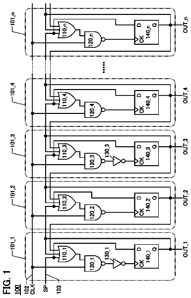
Shift register, semiconductor device, and electronic device
A semiconductor device and the like with low power consumption can be provided.
US 9,831,358 B2 · Assignee: I-SHOU UNIVERSITY · Inventors: Chiang; Jung-Sheng et al.
Sheet 1 of 13 from the published document. All sheets in the USPTO PDF
A photoelectric conversion device including a photoelectric converter, a transparent cover, an insulating material layer and a photonic crystal layer is provided. The photoelectric converter is adapted to receive a light. The transparent cover is disposed on a side of the photoelectric converter. The insulating material layer is disposed between the photoelectric converter and the transparent cover. The photonic crystal layer is disposed between the insulating material layer and the transparent cover, wherein the material of the photonic crystal layer is different from the material of the insulating material layer.
Field of the Invention The invention is related to an energy conversion device, and more particularly to a photoelectric conversion device. Description of Related Art After many years of development in solar cell technology, the power conversion efficiency, the stability, and the performance indices of the solar cells are greatly improved. Currently, the solar cells developed in laboratory can reach a fairly high photoelectric conversion efficiency, but the manufacturing process of the high photoelectric conversion efficiency solar cells is highly complex and expensive, so that it is very difficult to achieve mass production. Therefore, lower cost in production and higher photoelectric conversion efficiency are the important topics in developing solar cells. In practice, the photoelectric conversion efficiency of the solar cells depends on the external quantum efficiency (EQE) and the li
1 of 13 drawing sheets so far from the published document, cropped to the drawing. Every sheet is in the USPTO PDF.
What the patent claimed, word for word. All of it is now free to use.
This application claims the priority benefit of Taiwan application serial no. 104115563, filed on May 15, 2015. The entirety of the above-mentioned patent application is hereby incorporated by reference herein and made a part of specification.
Field of the Invention
The invention is related to an energy conversion device, and more particularly to a photoelectric conversion device.
Description of Related Art
After many years of development in solar cell technology, the power conversion efficiency, the stability, and the performance indices of the solar cells are greatly improved. Currently, the solar cells developed in laboratory can reach a fairly high photoelectric conversion efficiency, but the manufacturing process of the high photoelectric conversion efficiency solar cells is highly complex and expensive, so that it is very difficult to achieve mass production. Therefore, lower cost in production and higher photoelectric conversion efficiency are the important topics in developing solar cells. In practice, the photoelectric conversion efficiency of the solar cells depends on the external quantum efficiency (EQE) and the light absorption. In addition, the light absorption is increased when the quantity of incident light, an important factor, is increased. The light absorption are enhanced via the design to increase the quantity of incident light to the inside elements, so as to increase the photoelectric conversion efficiency of the solar cells.
The invention provides a photoelectric conversion device including a photoelectric converter, a transparent cover, an insulating material layer and a photonic crystal layer. The photoelectric converter is adapted to receive a light. The transparent cover is disposed on a side of the photoelectric converter. The insulating material layer is disposed between the photoelectric converter and the transparent cover. The photonic crystal layer is disposed between the insulating material layer and the transparent cover, wherein the material of the photonic crystal layer is different from the material of the insulating material layer.
In one embodiment of the invention, the insulating material layer is a flat plate, and the photonic crystal layer includes a plurality of first cavities perpendicularly extended from a surface of the photoelectric converter, wherein the first cavities are periodically arranged.
In one embodiment of the invention, the first cavities are cylindrical cavities or conical cavities.
In one embodiment of the invention, the photonic crystal layer includes a plurality of the first cavities extended in a direction perpendicular to a surface of the photoelectric converter. The insulating material layer includes a plurality of second cavities extended in the direction perpendicular to the surface of the photoelectric converter, wherein the first cavities are periodically arranged, and the second cavities are periodically arranged.
In one embodiment of the invention, the first cavities are cylindrical cavities or conical cavities.
In one embodiment of the invention, the second cavities are cylindrical cavities or conical cavities.
In one embodiment of the invention, the first cavities are periodically arranged, and the second cavities are periodically arranged. The central axis of the first cavity and the central axis of the second cavity are substantially coincident in a direction perpendicular to the surface of the photoelectric converter.
In one embodiment of the invention, the first cavities are periodically arranged, and the second cavities are periodically arranged. The central axis of the first cavity and the central axis of the second cavity are not substantially coincident in a direction perpendicular to the surface of the photoelectric converter.
In one embodiment of the invention, the material of the insulating material layer includes titanium dioxide or silicon dioxide.
In one embodiment of the invention, the material of the photonic crystal layer includes silicon dioxide or titanium dioxide.
Based on the above, in the photoelectric conversion device of the embodiments in the invention, the insulating material layer is disposed between the photoelectric converter and the transparent cover, the photonic crystal layer is disposed between the insulating material layer and the transparent cover, and the material of the photonic crystal layer is different from the material of the insulating material layer, so as to increase the quantity of incident light of the photoelectric converter.
In order to make the aforementioned and other features and advantages of the invention more comprehensible, embodiments accompanying figures are described in detail below.
FIG. 1 is a cross-sectional view depicting a simulation of a photoelectric conversion device of one comparative embodiment and setting conditions of finite-difference time-domain method.
FIG. 2 is a cross-sectional view depicting a simulation of a photoelectric conversion device of another comparative embodiment.
FIG. 3 is a graph depicting the simulation results of energy flux and normalized frequency of the photoelectric conversion device 100 in FIG. 2 and the photoelectric conversion device 50 in FIG. 1 .
FIG. 4A is a cross-sectional view depicting a simulation of a photoelectric conversion device of one embodiment in the invention.
FIG. 4B is an enlarged cross-sectional view depicting a photonic crystal layer 500 a in simulation in FIG. 4A .
FIG. 4C is a cross-sectional view depicting a simulation of a photoelectric conversion device of another embodiment in the invention.
FIG. 4D is a cross-sectional view depicting a simulation of a photoelectric conversion device of another embodiment in the invention.
FIG. 4E is an enlarged cross-sectional view depicting a photonic crystal layer 500 b in the simulation in FIG. 4D .
FIG. 4F is a graph depicting the simulation results of energy flux and normalized frequency of the photoelectric conversion device 100 a in FIG. 4A and the photoelectric conversion device 100 b in FIG. 4C .
FIG. 4G is a graph depicting the simulation results of energy flux and normalized frequency of the photoelectric conversion device 100 b in FIG. 4C and the photoelectric conversion device 100 c in FIG. 4D .
FIG. 5A is a cross-sectional view depicting a simulation of a photoelectric conversion device of another embodiment in the invention.
FIG. 5B is an enlarged cross-sectional view depicting insulating material layer 400 a and the photonic crystal layer 500 a in the simulation in FIG. 5A .
FIG. 5C is a cross-sectional view depicting a simulation of a photoelectric conversion device of another embodiment in the invention.
FIG. 5D is a cross-sectional view depicting the enlarged insulating material layer 400 a and the photonic crystal layer 500 a in FIG. 5C .
FIG. 5E is a graph depicting the simulation results of energy flux and normalized frequency of the photoelectric conversion device 100 d in FIG. 5A and the photoelectric conversion device 100 e in FIG. 5C .
FIG. 6A is a cross-sectional view depicting a simulation of a photoelectric conversion device of another embodiment in the invention.
FIG. 6B is a cross-sectional view depicting the enlarged insulating material layer 400 b and the photonic crystal layer 500 b in FIG. 6A .
FIG. 6C is a cross-sectional view depicting a simulation of a photoelectric conversion device of another embodiment in the invention.
FIG. 6D is a cross-sectional view depicting the enlarged insulating material layer 400 b and the photonic crystal layer 500 b in FIG. 6C .
FIG. 6E is a graph depicting the simulation results of energy flux and normalized frequency of the photoelectric conversion device 100 f in FIG. 6A and the photoelectric conversion device 100 g in FIG. 6C .
FIG. 1 is a cross-sectional view depicting a simulation of a photoelectric conversion device of one comparative embodiment and setting conditions of finite-difference time-domain method. Referring to FIG. 1 , in the present embodiment, a photoelectric conversion device 50 includes a photoelectric converter 200 which is adapted to receive a light L. Specifically, the photoelectric converter 200 is silicon solar cells, or other folins of photoelectric device able to perfolin photoelectric conversion. In the present embodiment, in order to simulate the electromagnetic wave transmitting through the photoelectric conversion device 50 and to analyze the ratio of the received energies under different conditions, the finite-difference-time-domain method (FDTD method), an appropriate method to calculate the dynamic behavior of the electromagnetic wave, is used as a numerical analysis method, and cases having more complex boundary condition are also simulated. In the related embodiments of the invention, the FDTD method is used to analyze the electromagnetic wave transmitting through the photoelectric conversion device, but the invention is not limited thereto, other numerical methods appropriate to calculate the dynamic behavior of the electromagnetic wave can be used to analyze the photonic conversion device.
Referring to FIG. 1 , in the present embodiment, in order to prevent unable to calculate and non-physical reflection phenomenon, the photoelectric conversion device 50 further includes a perfectly matched layer PML to fulfil the absorbent boundary conditions. The simulated electromagnetic wave is not reflected when it propagates to the perfectly matched layer PML which is an artificial boundary, so that the simulation results are the same as in the real condition.
The table 1 below shows the initial settings of computational cell to simulate the photoelectric conversion device 50 in the present embodiment. It should be noted that the invention is not limited to the data listed in Table 1. It should be known to those ordinary skilled in the art that various modifications and variations can be made to the parameters or settings of the present invention without departing from the scope or spirit of the invention.
TABLE-US-00001 TABLE 1 The horizontal length of the computational 10 (μm) cell (Sx) The vertical length of the computational 32 (μm) cell (Sy) The relative permittivity of air 1 The thickness of the perfectly matched 1 (μm) layer (PML) The lattice constant (a) 1 (μm) The light source The Gaussian source The wavelength of the light source (λ) 0.6 μm The center frequency of the light source 1.67 The bandwidth of the light source 0.1
In the present embodiment, dimension is used by the finite-difference-time-domain method to calculate. The complex parameters, such as the absolute permittivity (ε.sub.0), the absolute permeability (μ.sub.0), the velocity of light (3×10^8 m/s, c) etc., can be normalized and set as 1, so as to analyze the simulation results through the ratio directly in the simulation process. Besides in the present embodiment, the Gaussian source is further adopted to serve as the light source LS in the simulation of the photoelectric conversion device 50 and emits the light L perpendicular to the photoelectric converter 200 . The light source of the embodiments in the invention is a Gaussian source which emits the light L perpendicular to the photoelectric converter, but the invention is not limited thereto. Other types of simulation light source emitting the light perpendicular to the photoelectric converter can be used. Besides, in the present embodiment and related embodiments in the invention, when the Gaussian source is set up, the center frequency and the bandwidth need being considered. Specifically, the lattice constant is set to 1. In addition, the frequency (f) of the incident wave, i.e., the ratio of the lattice constant to the incident light wavelength (λ) is presented by the normalized frequency, the settings of the normalized frequency is a/λ(=ωa/2πc.sub.0=fa/c.sub.0).
Referring to FIG. 1 and Table 1, in the present embodiment, the horizontal length of the computational cell (Sx) is set to 10 μm, the vertical length of the computational cell (Sy) is set to 32 μm. During the simulation, the photoelectric conversion device 50 is covered by the perfectly matched layer PML having thickness of 1 μm and located in the computational cell. Besides the position of the light receiving surface of the photoelectric converter 200 in the computational cell is the zero-point in the vertical axis coordinate. The region from one side facing the light source LS of the light receiving surface to the perfectly matched layer PML is a media having relative permittivity equal to 1, so as to simulate the air. In addition, the region from the other side of the light receiving surface to the perfectly matched layer PML is a media having relative permittivity equal to 12, so as to simulate the solar cells. Starting from the zero-point in the vertical axis coordinate, the fixed positions having 2 μm interval are arranged long the direction R perpendicular to the light receiving surface of the photoelectric converter 200 , such as ±2,±4, ±6, ±8, ±10, ±12, and ±14. The light L is emitted from the light source LS, and by the field pattern of the light L when transferring is calculated and simulated by the finite-difference-time domain method, the quantity of energy flux is calculated at different fixed positions respectively, so as to identify the degree of energy loss of the light L when passing though different fixed positions of the photoelectric conversion device 50 and to identify the degree of variation of the energy flux. The unit of the energy flux is Watts per square meter (W/m.sup.2), so that the energy value, its unit is Watt (W), can be obtained by surface integral of unit size of the computational cell.
In the present embodiment, when the photoelectric conversion device 50 is simulated by the finite-difference-time domain method under the above-mentioned conditions, a surface receiving light L is located in the photoelectric converter 200 at the −2 μm position along the vertical direction (the position inside the photoelectric converter 200 ) to serve as a light receiving area R, so as to calculate the energy flux of the light L passing through the photoelectric converter to be a reference value, and to prevent unnecessary effect and interference. In the present embodiment, to be more specific, the calculated energy flux at receiving area R of the photoelectric conversion device 50 is 29.99502167 Watts per square meter (W/m.sup.2). If the original simulating the photoelectric conversion device 50 is changed to simulating the air, namely, the perfectly matched layer PML only contains the media having the media having relative permittivity equal to 1 in the simulation environment, the calculated energy flux at a position the same as the receiving area R is 40.68963037 Watts per square meter. The energy transmission rate can be calculated by dividing the calculated energy flux at at receiving area R of the photoelectric conversion device 50 by the calculated energy flux at receiving area R of the air. Namely, 29.99502167 Watts per square meter is divided by 45.65358650 Watts per square meter and multiplied by 100%, so as to obtain that the energy transmission rate is equal to 65.7%. It should be noted that, the value of the energy flux and the energy transmission rate is calculated as an example under the above-mentioned setting conditions and should not be used to limit the scope of the invention.
FIG. 2 is a cross-sectional view depicting a simulation of a photoelectric conversion device of another embodiment of the invention. Referring to FIG. 2 , in the present embodiment, the photoelectric conversion device 100 includes the photoelectric converter 200 , a transparent cover 300 , an insulating material layer 400 . Besides, the photoelectric conversion device 100 also includes an insulating material layer 400 ′. The photoelectric converter 200 is the same as the photoelectric converter 200 of the photoelectric conversion device 500 of the comparative embodiment. The transparent cover 300 is disposed on a side of the photoelectric converter 200 . The insulating material layer 400 is disposed between the photoelectric converter 200 and the transparent cover 300 . The insulating material layer 400 ′ is configured between the transparent cover 300 and the insulating material layer 400 which are passed through by the light L. In the present comparative embodiment, specifically, the detailed structure of the photoelectric converter 200 further includes an N type semiconductor layer 210 , a P type semiconductor layer 220 , and an electrode layer 230 . The P type semiconductor layer 220 is located between the N type semiconductor layer 210 and the electrode layer 230 , and the N type semiconductor layer 210 is located between the insulating material layer 400 and the P type semiconductor layer 220 . In some embodiments, the position of the N type semiconductor layer 210 and the position of the P type semiconductor layer can be interchanged; that is, the N type semiconductor layer 210 is located between the P type semiconductor layer 220 and the electrode layer 230 , and the P type semiconductor layer 220 is located between the insulating material layer 400 and the N type semiconductor layer 210 . In addition, in some embodiments, a patterning electrode (not shown) is in between the photoelectric converter 200 and the insulating material layer 400 . The insulating material layer 400 can be located between the insulating material layer 400 ′ and an area without electrode of the patterning electrode, and the insulating material layer 400 also can be located between the insulating material layer 400 ′ and the whole patterning electrode. In the related embodiments of the invention, the photoelectric converter can include the above-mentioned detailed structure, but the invention is not limited thereto. The photoelectric converter in the relative embodiments further includes, for example, an antireflection layer or a structure adapted to apply to the photoelectric converter.
In the present compared embodiments, the material of the insulating material layer 400 ′ is different from the material of the insulating material layer 400 . Specifically, the material of the insulating material layer 400 includes titanium dioxide (TiO.sub.2), or silicon dioxide (SiO.sub.2 or silica), and the material of the insulating material layer 400 ′ includes silicon dioxide, or titanium dioxide. Generally, when the light L enters the solar cells having different material flat plates which are superimposed to obtain an effect that the index of refraction is gradually changed, the reflected light part is reduced and a large quantity of light energy enters solar cells. Therefore, the insulating material layer 400 , the insulating material layer 400 ′, and photoelectric converter 200 in the invention are superimposed and made by different materials, so that the index of refraction is gradually changed from the insulating material layer 400 through the insulating material layer 400 ′ to photoelectric converter 200 . When the light entering the titanium dioxide has wavelength equal to 6 μm, the index of refraction of the titanium dioxide is greater than the index of refraction of the silicon dioxide, so that the insulating material layer 400 is the titanium dioxide flat plate, which is located on the surface S of the photoelectric converter 200 receiving the light L, and the insulating material layer 400 ′ is the silicon dioxide flat plate. In the present embodiment, the photoelectric converter 200 is solar cell which is simulated by the finite-difference-time-domain method with the relative permittivity is set to 12, the same as in the simulation of the photoelectric converter 50 in FIG. 1 . The transparent cover 300 serves as a light receiving surface of a protection layer of the photoelectric converter 200 , the material of the transparent cover 300 includes glass or other materials having a high light transmission property. In the present embodiment, transparent cover 300 is simulated by the finite-difference-time domain method with the relative permittivity is set to 1, the same as in the simulation of the air. Hence, the photoelectric conversion device 500 and 100 can be simulated with and without the insulating material layer 400 and the insulating material layer 400 ′ for comparison purposes.
In the present comparative embodiment, the photoelectric conversion device 100 is placed in a simulation environment which is the same as the simulation environment of the photoelectric conversion device 50 . The simulation of the photoelectric conversion device 100 also includes simulating the perfectly matched layer PML which is used to fulfil the absorbent boundary conditions, and a surface receiving light L is located at the photoelectric converter 200 at the −2 μm position along the vertical direction (the position inside the photoelectric converter 200 ) to serve as a light receiving area R. The detail settings for the computational cell to simulate the energy flux of the photoelectric conversion device 100 by the finite-difference-time-domain method are referenced to the FIG. 1 and Table 1, and will not be repeated.
FIG. 3 is a graph depicting the simulation results of energy flux and normalized frequency of photoelectric conversion device 100 in FIG. 2 and photoelectric conversion device 50 in FIG. 1 . Referring to FIG. 3 , in the present comparative embodiment, based on the results calculated by the finite-difference-time-domain method, the calculated energy flux at receiving area R of the photoelectric conversion device 100 , which has the titanium dioxide flat plate serving as the insulating material layer 400 and has the silicon dioxide flat plate serving as the insulating material layer 400 ′, is equal to 34.83107839 Watts per square meter. Considering the photoelectric conversion device 500 which does not include the insulating material layer 400 and the insulating material layer 400 ′ of the embodiment in FIG. 1 , the energy transmission rate can be calculated by dividing the calculated energy flux at receiving area R of the photoelectric conversion device 100 by the calculated energy flux at receiving area R of the photoelectric conversion device 50 . Namely, 34.83107839 Watts per square meter is divided by 29.99502167 Watts per square meter and multiplied by 100%, so as to obtain that the energy transmission rate is equal to 116.12%. On the contrary, the perfectly matched layer PML only contains the media having the media having relative permittivity equal to 1 in the simulation environment, the energy transmission rate can be calculated by dividing the calculated energy flux at receiving area R of the photoelectric conversion device 100 by the calculated energy flux at receiving area R of the air. Namely, 34.83107839 Watts per square meter is divided by 45.65358650 Watts per square meter and multiplied by 100%, so as to obtain that the energy transmission rate is equal to 76.3%. It is described in FIG. 3 that, the energy flux at the receiving area R of the photoelectric conversion device 100 is greater than the energy flux at the receiving area R of the photoelectric conversion device 50 . In the present comparative embodiment, the photoelectric conversion device 100 including the titanium dioxide flat plate and the silicon dioxide flat plate has a larger quantity of incident light than the photoelectric conversion device 50 having none of the flat plate.
FIG. 4A is a cross-sectional view depicting a simulation of a photoelectric conversion device of one embodiment in the invention. Referring to FIG. 4A , in the present embodiment, the photoelectric conversion device 100 a is similar to the photoelectric conversion device 100 , the main elements of the photoelectric conversion device 100 a can be referenced from the photoelectric conversion device 100 and will not be repeated. The difference is that, the photonic conversion device 100 a does not include the insulating material layer 400 and the insulating material layer 400 ′, and the photoelectric conversion device 100 a further includes a photonic crystal layer 500 a , the photonic crystal layer 500 a includes a plurality of first cavities 510 a extended in a direction perpendicular to a surface S of the photoelectric converter 200 , wherein the first cavities 510 a are periodically arranged. The first cavities 510 a are, for example, cylindrical cavities, or conical cavities, or cavities having other shapes.
FIG. 4B is an enlarged cross-sectional view depicting a photonic crystal layer 500 a in simulation in FIG. 4A . Referring to FIG. 4B and FIG. 4A , specifically, in the present embodiment, the first cavities 510 a are cylindrical cavities, and the ratio of the diameter dcy to the depth Dcy of the cylindrical cavities is from 0.5 to 0.9. Besides, the pitch Pcy of two adjacent first cavities 510 a is from 1 to 1.2 micrometer (μm). In the present embodiment, the material of the photonic crystal layer 500 a having the first cavities 510 a with periodic property is silicon dioxide.
FIG. 4 is a cross-sectional view depicting a simulation of a photoelectric conversion device of another embodiment in the invention. Referring to FIG. 4C , in the present embodiment, the photoelectric conversion device 100 b is similar to the photoelectric conversion device 100 a , the main elements of the photoelectric conversion device 100 b can be referenced from the photoelectric conversion device 100 a and will not be repeated. The different is that, the photoelectric conversion device 100 b includes the insulating material layer 400 . In the present embodiment, the insulating material layer 400 is disposed between the photonic crystal layer 500 a and the photoelectric converter 200 , and the insulating material layer 400 includes a titanium dioxide flat plate.
FIG. 4D is a cross-sectional view depicting a simulation of a photoelectric conversion device of another embodiment in the invention. Referring to FIG. 4D , in the present embodiment, the photoelectric conversion device 100 c is similar to the photoelectric conversion device 100 b , the main elements of the photoelectric conversion device 100 c can be referenced from the photoelectric conversion device 100 b and will not be repeated. The difference is that, the photonic crystal layer 500 b of the photoelectric conversion device 100 c includes a plurality of first cavities 510 b extended in the direction perpendicular to the surface S of the photoelectric converter 200 , wherein the first cavities 510 b are periodically arranged. The first cavities 510 b are, for example, cylindrical cavities, or conical cavities, or cavities having other shapes.
FIG. 4E is an enlarged cross-sectional view depicting a photonic crystal layer 500 b in the simulation in FIG. 4D . Referring to FIG. 4D and FIG. 4E , specifically, in the present embodiment, the first cavities 510 b can be conical cavities, and the ratio of the diameter dta of the conical cavities to the depth of the conical cavities is from 0.5 to 0.9. Besides, the pitch Pta of two adjacent first cavities 510 b is from 1 to 1.2 μm. In the present embodiment, the material of the photonic crystal layer 500 b having the first cavities 510 b with periodic property is silicon dioxide, and the insulating material layer 400 includes a titanium dioxide flat plate.
FIG. 4F is a graph depicting the simulation results of energy flux and normalized frequency of the photoelectric conversion device 100 a in FIG. 4A and the photoelectric conversion device 100 b in FIG. 4C . Referring to FIG. 4F , in the present embodiment, the photoelectric conversion device 100 a and the photoelectric conversion device 100 b are placed in a simulation environment which is the same as the simulation environment of the photoelectric conversion device 50 in FIG. 1 . The simulation of the photoelectric conversion device 100 a and the photoelectric conversion device 100 b also includes simulating the perfectly matched layer PML which is used to fulfil the absorbent boundary conditions, and the surface receiving light L is located at the photoelectric converter 200 at the −2 μm position along the vertical direction (the position inside the photoelectric converter 200 ) to serve as the light receiving area R. The detail settings for the computational cell to simulate the energy flux of the photoelectric conversion device 100 a and the photoelectric conversion device 100 b by the finite-difference-time-domain method are referenced to the FIG. 1 and Table 1, and will not be repeated.
In the present embodiment, the photoelectric conversion device 100 a includes the photonic crystal layer 500 a formed by cylindrical cavities having periodic property. After the simulation by the finite-difference-time-domain method, the calculated energy flux at receiving area R of the photoelectric conversion device 100 a is equal to 40.68963037 Watts per square meter. Besides, in one embodiment of the invention, the insulating material layer 400 of the photoelectric conversion device 100 b is a titanium dioxide flat plate, and the photonic crystal layer 500 b of the photoelectric conversion device 100 b is conical cavities having periodic property. After the simulation by the finite-difference-time-domain method, the calculated energy flux at receiving area R of the photoelectric conversion device 100 b is equal to 42.28312740 Watts per square meter. The energy transmission rate relatively between the photoelectric conversion device 100 b and the photoelectric conversion device 100 a can be calculated by dividing the calculated energy flux at receiving area R of the photoelectric conversion device 100 b by the calculated energy flux at receiving area R of the photoelectric conversion device 100 a . Namely, 42.28312740 Watts per square meter is divided by 40.68963037 Watts per square meter and multiplied by 100%, so as to obtain that the energy transmission rate is equal to 103.92%. In the present embodiment, the energy transmission rate between the photoelectric conversion device 100 b , which has the cylindrical cavities having periodic property to serve as the photonic crystal layer 500 a , and the media (the air) having the media having relative permittivity equal to 1, which is only contained by the perfectly matched layer PML, can be calculated by dividing the calculated energy flux at receiving area R of the photoelectric conversion device 100 b by the calculated energy flux at receiving area R of the air, so as to obtain that the energy transmission rate is equal to 92.6%. In FIG. 4F , the silicon dioxide cylindrical cavities present the cylindrical cavities having periodic property which serve as the photonic crystal layer 500 a of the photoelectric conversion device 100 a , and the photoelectric conversion device does not include the insulating material layer 400 . Moreover, the silicon dioxide cylindrical cavities and the titanium dioxide flat plate present the photoelectric conversion device 100 b of one embodiment in the invention. In the photoelectric conversion device 100 b , the cylindrical cavities having periodic property serve as the photonic crystal layer 500 a , and the titanium dioxide flat plate serve as the insulating material layer 400 . It is described in FIG. 4F that, the energy flux at the receiving area R of the photoelectric conversion device 100 b is greater than the energy flux at the receiving area R of the photoelectric conversion device 100 a . In the present embodiment, the photoelectric conversion device 100 b , which has the photonic crystal layer 500 a made by the cylindrical cavities having periodic property and has the insulating material layer 400 made by the titanium dioxide flat plate, has a larger quantity of incident light than the photoelectric conversion device 100 a , which does not include the insulating material layer 400 made by the titanium dioxide flat plate. Moreover, compared to the embodiment in FIG. 2 and FIG. 3 wherein the energy transmission rate relatively between the photoelectric conversion device 100 and the air is equal to 76.3%, the energy transmission rate relatively between the photoelectric conversion device 100 b and the air is equal to 92.6%, so that the photoelectric conversion device 100 b has a larger quantity of incident light.
FIG. 4G is a graph depicting the simulation results of energy flux and normalized frequency of the photoelectric conversion device 100 b in FIG. 4C and the photoelectric conversion device 100 c in FIG. 4D . Referring to FIG. 4G , in the present embodiment, the photoelectric conversion device 100 b and the photoelectric conversion device 100 c are placed in a simulation environment which is the same as the simulation environment of the photoelectric conversion device 50 in FIG. 1 . The simulation of the photoelectric conversion device 100 b and the photoelectric conversion device 100 c also includes simulating the perfectly matched layer PML which is used to fulfil the absorbent boundary conditions, and a surface receiving light L is located at the photoelectric converter 200 at the −2 μm position along the vertical direction (the position inside the photoelectric converter 200 ) to serve as a light receiving area R. The detail settings for the computational cell to simulate the energy flux of the photoelectric conversion device 100 b and the photoelectric conversion device 100 c by the finite-difference-time-domain method are referenced to the FIG. 1 and Table 1, and will not be repeated.
In the present embodiment, the results calculated by the finite-difference-time-domain method of the photoelectric conversion device 100 b is the same as the results shown in FIG. 4F , the calculated energy flux at receiving area R of the photoelectric conversion device 100 b is equal to 42.28312740 Watts per square meter. Besides, the insulating material layer 400 of the photoelectric conversion device 100 c is a titanium dioxide flat plate, but the photonic crystal layer 500 b of the photoelectric conversion device 100 c is conical cavities having periodic property. After the simulation by the finite-difference-time-domain method, the calculated energy flux at receiving area R of the photoelectric conversion device 100 c is equal to 39.59895216 Watts per square meter. The energy transmission rate relatively between the photoelectric conversion device 100 b and the photoelectric conversion device 100 c can be calculated by dividing the calculated energy flux at receiving area R of the photoelectric conversion device 100 b by the calculated energy flux at receiving area R of the photoelectric conversion device 100 c . Namely, 42.28312740 Watts per square meter is divided by 39.59895216 Watts per square meter and multiplied by 100%, so as to obtain that the energy transmission rate is equal to 106.78%. In FIG. 4G , the cylindrical cavities present the cylindrical cavities having periodic property which serve as the photonic crystal layer 500 a of the photoelectric conversion device 100 b . Moreover, the conical cavities present the conical cavities having periodic property which serve as the photonic crystal layer 500 b of the photoelectric conversion device 100 c . It is described in FIG. 4G that, the energy flux at the receiving area R of the photoelectric conversion device 100 b is greater than the energy flux at the receiving area R of the photoelectric conversion device 100 c . In the present embodiment, the photoelectric conversion device 100 b , which has the photonic crystal layer 500 a made by the cylindrical cavities having periodic property, has a larger quantity of incident light than the photoelectric conversion device 100 c , which has the photonic crystal layer 500 b made by the conical cavities having periodic property.
FIG. 5A is a cross-sectional view depicting a simulation of a photoelectric conversion device of another embodiment in the invention. FIG. 5B is an enlarged cross-sectional view depicting an insulating material layer 400 a of the photonic crystal layer 500 a in FIG. 5A . Referring to FIG. 5A and FIG. 5B , in the present embodiment, the photoelectric conversion device 100 d is similar to the photoelectric conversion device 100 b and the photonic crystal layer 500 a of the photoelectric conversion device 100 d includes a plurality of first cavities 510 a extended in the direction perpendicular to the surface S of the photoelectric converter 200 , the first cavities 510 a are periodically arranged, and the first cavities 510 a are, for example, cylindrical cavities, or conical cavities, or cavities having other shapes. The main elements of the photoelectric conversion device 100 d can be referenced from the photoelectric conversion device 100 b and will not be repeated. The difference is that, the insulating material layer 400 a of the photonic conversion device 100 d includes a plurality of second cavities 410 a extended in the direction perpendicular to the surface S of the photoelectric converter 200 , the second cavities 410 a are periodically arranged, and the second cavities 410 a are, for example, cylindrical cavities, or conical cavities, or cavities having other shapes.
Specifically, in the present embodiment, the first cavities 510 a of the photoelectric conversion device 100 d can be cylindrical cavities, and the ratio of the diameter dcy to the depth Dcy and the pitch Pcy of two adjacent first cavities 510 a can be referenced to the photoelectric conversion device 100 b in FIG. 4B and FIG. 4C . The second cavities 410 a of the photoelectric conversion device 100 d can be the cylindrical cavities, and the ratio of the diameter dcy to the depth Dcy of the cylindrical cavities 410 a is from 0.5 to 0.9. The pitch Pcy of two adjacent second cavities 410 a is from 1 to 1.2 μm. In the present embodiment, the material of the photonic crystal layer 500 a having the first cavities 510 b with periodic property is silicon dioxide, and the material of the insulating material layer 400 a having the second cavities 410 a with periodic property is titanium dioxide. Specifically, the central axis A 1 of the first cavity 510 a and the central axis A 2 of the second cavity 410 a are substantially coincident in a direction perpendicular to the surface S of the photoelectric converter 200 , and the first cavity 510 a and the second cavity 410 a are aligned.
FIG. 5C is a cross-sectional view depicting a simulation of a photoelectric conversion device of another embodiment in the invention. FIG. 5D is an enlarged cross-sectional view depicting an insulating material layer 400 a of the photonic crystal layer 500 a in the simulation in FIG. 5C . Referring to FIG. 5C and FIG. 5D , in the present embodiment, the photoelectric conversion device 100 e is similar to the photoelectric conversion device 100 d , the main elements of the photoelectric conversion device 100 e can be referenced from the photoelectric conversion device 100 d and will not be repeated. The difference is that, the central axis A 1 of the first cavity 510 a and the central axis A 2 of the second cavity 410 a of the photoelectric conversion device 100 e are not substantially coincident in a direction perpendicular to the surface S of the photoelectric converter 200 , and the first cavity 510 a and the second cavity 410 a are not aligned.
The description continues in the full USPTO document.
About 6,355 words. The USPTO PDF has it with every drawing.
Fees are due 3.5, 7.5 and 11.5 years after grant. This patent expired on November 28, 2025, so the fee marked "not paid" was the one that went unpaid.
PHOTOELECTRIC CONVERSION DEVICE
Filed Sep 2015 · published Nov 2016Photoelectric conversion device
Filed Sep 2015 · granted Nov 2017Earlier publications, parents and continuations. None of them can still be enforced, or this patent would not be listed.
Prior art cited by the examiner or applicant. Useful when you check your own idea for novelty.
Everything on this page comes from the documents linked above.


