Cross-reference to related applications
The disclosure of Japanese Patent Application No. 2015-070152 filed on Mar. 30, 2015 including the specification, drawings and abstract is incorporated herein by reference in its entirety.
Background
The present invention relates to a semiconductor device and a method for manufacturing the same, and can be suitably used for example for a semiconductor device including a non-volatile memory and a method for manufacturing the same.
As an electrically writable/erasable non-volatile semiconductor storage device, an EEPROM (Electrically Erasable and Programmable Read Only Memory) has been widely used. These storage devices represented by a flash memory widely used at present include an electro-conductive floating gate electrode surrounded by an oxidized film under a gate electrode of a MISFET or a trapping insulating film, and the electric charge storage state in the floating gate or the trapping insulating film is made the storage information which is read as a threshold value of the transistor. This trapping insulating film means an insulating film capable of storing the electric charge, and a silicon nitride film and the like can be cited as an example. By charging/discharging of the electric charge to/from such an electric charge storage region, the threshold value of the MISFET is shifted, and the MISFET is operated as a storage element. As the flash memory, there is a split gate type cell using a MONOS (Metal-Oxide-Nitride-Oxide-Semiconductor) film. In such memory, by using the silicon nitride film as the electric charge storage region, such advantages are provided of being excellent in reliability in holding data for discretely storing the electric charge compared to the electro-conductive floating gate film, being capable of thinning the oxide films over and below the silicon nitride film because of the excellent reliability in holding data, being capable of lowering the voltage of the writing/erasing operation, and so on.
Also, the memory cell includes a control gate electrode (selection gate electrode) that is formed over a semiconductor substrate through a first gate insulating film, a memory gate electrode that is formed over the semiconductor substrate through a second gate insulating film including an electric charge storage region, and a pair of semiconductor regions (a source region and a drain region) that are formed over the surface of the semiconductor substrate so as to sandwich the control gate electrode and the memory gate electrode. In the memory cell region, plural memory cells are disposed in a matrix shape in the X-direction and the Y-direction. For example, with respect to plural memory cells arrayed in a row in the Y-direction, the control gate electrode and the memory gate electrode are respectively formed integrally, and the control gate electrode and the memory gate electrode extend in the Y-direction. For example, the control gate electrode and the memory gate electrode comprised of a polycrystalline silicon film and the like extend to an electric supply region (shunt region) adjacent to the memory cell region, and are coupled there with a control gate line (selection gate line) and a memory gate line which are comprised of a metal wiring layer for example.
In Japanese Unexamined Patent Application Publication No. 2006-049737, Japanese Unexamined Patent Application Publication No. 2011-222938, and Japanese Unexamined Patent Application Publication No. 2006-054292, technologies on a shunt structure for coupling the control gate electrode with the control gate line and coupling the memory gate electrode with the memory gate line in the electric supply region are described.
Summary
Also in the semiconductor device including a non-volatile memory, it is desired to improve the performance as much as possible, or to improve the reliability of the semiconductor device, or to achieve the both of them.
Other problems and new features will be clarified from the description of the present specification and the attached drawings.
According to an embodiment, a semiconductor device includes a semiconductor substrate that includes a memory cell region in the main surface of the semiconductor substrate and a shunt region that is adjacent to the memory cell region in a first direction of the main surface. Also, the semiconductor device includes a memory cell that is formed in the memory cell region, the memory cell including a first gate electrode that is formed over the main surface of the semiconductor substrate through a first gate insulating film and extends in the first direction, a second gate electrode that is adjacent to the first gate electrode and is formed over the main surface of the semiconductor substrate through a second gate insulating film, and a first source region and a first drain region that are formed over the main surface of the semiconductor substrate so as to sandwich the first gate electrode and the second gate electrode. Further, the semiconductor device includes a first electrode that is positioned in the shunt region and is formed integrally with the first gate electrode, and a second electrode that is positioned in the shunt region, is formed integrally with the second gate electrode, and includes a first section formed along the side wall of the first gate electrode and a second section extending from the first section along the main surface of the semiconductor substrate. Also, the semiconductor device includes a first insulating film that covers the first gate electrode, the second gate electrode, the first electrode, and the second electrode, an electro-conductive first plug and an electro-conductive second plug that are formed in the first insulating film with the first plug being coupled with the drain region and with the second plug being coupled with the second electrode, and a first metal wiring and a second metal wiring which are positioned over the first insulating film with the first metal wiring being coupled with the first plug and with the second metal wiring being coupled with the second plug. Further, with respect to the main surface of the semiconductor substrate, the height of the upper surface of the first electrode is generally same to the height of the upper surface of the first section of the second electrode.
According to the embodiment, the performance of the semiconductor device can be improved, or the reliability of the semiconductor device can be improved, or the both of them can be achieved.
Brief description of the drawings
FIG. 1 is a process flowchart showing a part of the manufacturing step of a semiconductor device that is an embodiment.
FIG. 2 is a process flowchart showing a part of the manufacturing step of the semiconductor device that is an embodiment.
FIG. 3 is a process flowchart showing a part of the manufacturing step of the semiconductor device that is an embodiment.
FIG. 4 is a cross-sectional view of an essential part during the manufacturing step of a semiconductor device of an embodiment.
FIG. 5 is a cross-sectional view of an essential part during the manufacturing step of the semiconductor device following FIG. 4 .
FIG. 6 is a cross-sectional view of an essential part during the manufacturing step of the semiconductor device following FIG. 5 .
FIG. 7 is a cross-sectional view of an essential part during the manufacturing step of the semiconductor device following FIG. 6 .
FIG. 8 is a cross-sectional view of an essential part during the manufacturing step of the semiconductor device following FIG. 7 .
FIG. 9 is a cross-sectional view of an essential part during the manufacturing step of the semiconductor device following FIG. 8 .
FIG. 10 is a cross-sectional view of an essential part during the manufacturing step of the semiconductor device following FIG. 9 .
FIG. 11 is a cross-sectional view of an essential part during the manufacturing step of the semiconductor device following FIG. 10 .
FIG. 12 is a cross-sectional view of an essential part during the manufacturing step of the semiconductor device following FIG. 11 .
FIG. 13 is a cross-sectional view of an essential part during the manufacturing step of the semiconductor device following FIG. 12 .
FIG. 14 is a cross-sectional view of an essential part during the manufacturing step of the semiconductor device following FIG. 13 .
FIG. 15 is a cross-sectional view of an essential part during the manufacturing step of the semiconductor device following FIG. 14 .
FIG. 16 is a cross-sectional view of an essential part during the manufacturing step of the semiconductor device following FIG. 15 .
FIG. 17 is a cross-sectional view of an essential part during the manufacturing step of the semiconductor device following FIG. 16 .
FIG. 18 is a cross-sectional view of an essential part during the manufacturing step of the semiconductor device following FIG. 17 .
FIG. 19 is a cross-sectional view of an essential part during the manufacturing step of the semiconductor device following FIG. 18 .
FIG. 20 is a cross-sectional view of an essential part during the manufacturing step of a semiconductor device that is an embodiment other than FIG. 19 .
FIG. 21 is a cross-sectional view of an essential part during the manufacturing step of the semiconductor device following FIG. 19 .
FIG. 22 is a cross-sectional view of an essential part of a semiconductor device that is an embodiment.
FIG. 23 is a cross-sectional view of an essential part of a semiconductor device that is an embodiment.
Detailed description
In the embodiments below, when it is required for the sake of convenience, although description will be made dividedly into plural sections or embodiments, they are not unrelated to each other, and one has a relationship of a modification, detail, supplementary explanation and the like of a part or entirety with the other with the exception of a case particularly stated explicitly. Further, in the embodiments below, when the quantity of elements and the like (including the number of pieces, numerical value, amount, range and the like) are mentioned, they are not limited to the quantity mentioned and may be equal to or more than and equal to or less than the quantity mentioned with the exception of a case particularly specified explicitly, a case apparently limited to a specific quantity in principle, and so on. Further, in the embodiments below, it is needless to mention that the constituent elements thereof (also including the elemental step and the like) are not necessarily indispensable with the exception of a case particularly specified explicitly, a case considered to be apparently indispensable in principle, and so on. In a similar manner, in the embodiments below, when the shape, the positional relation and the like of a constituent element and the like are mentioned, they are to contain one that is substantially approximate or similar to the shape and the like thereof and so on with the exception of a case particularly specified explicitly, a case apparently considered not to be the case in principle, and so on. This fact also applies to the numerical value and the range described above.
Below, the embodiment will be explained in detail based on the drawings. Also, in all drawings for explaining the embodiment, a same reference sign will be given to a member having a same function, and repeated explanation thereon will be omitted. Further, in the embodiments below, explanation on a same or similar portions will not be repeated in principle except when it is particularly required.
Also, in the drawings used in the embodiment, there is also a case hatching is omitted even in a cross-sectional view in order to facilitate understanding of the drawing. Further, there is also a case hatching is given even in a plan view in order to facilitate understanding of the drawing. Embodiment
<On Manufacturing Step of Semiconductor Device>
The semiconductor device of the present embodiment and embodiments below is a semiconductor device including a non-volatile memory (non-volatile storage element, flash memory, non-volatile semiconductor storage device). In the present embodiment and the embodiments below, the non-volatile memory will be explained based on a memory cell that is based on an n-channel type MISFET (MISFET: Metal Insulator Semiconductor Field Effect Transistor).
The method for manufacturing the semiconductor device of the present embodiment will be explained referring to the drawings.
FIG. 1 to FIG. 3 are the process flowcharts showing a part of the manufacturing step of the semiconductor device of the present embodiment. FIG. 4 to FIG. 21 are the cross-sectional views of an essential part during the manufacturing step of the semiconductor device of the present embodiment. Also, in the cross-sectional views of FIG. 4 to FIG. 21 , the cross-sectional views of an essential part of a memory cell region 1 A, a peripheral circuit region 1 B, and a shunt region SH are shown, and the states of forming a memory cell of a non-volatile memory in the memory cell region 1 A, a MISFET in the peripheral circuit region 1 B, and a shunt structure in the shunt region SH respectively in a semiconductor substrate SB are shown.
The memory cell region 1 A, the peripheral circuit region 1 B, and the shunt region SH exist in the same semiconductor substrate SB. In the cross-sectional views of FIG. 4 to FIG. 21 , the memory cell region 1 A, the peripheral circuit region 1 B, and the shunt region SH are illustrated in this order, however, the memory cell region 1 A and the peripheral circuit region 1 B as well as the peripheral circuit region 1 B and the shunt region SH may not be adjacent to each other.
In the memory cell region 1 A, plural split gate type memory cells are disposed in a matrix shape, and the memory cell is comprised of an n-channel type MISFET (a control transistor and a memory transistor). The memory cell includes a control gate electrode that is formed over a semiconductor substrate through a gate insulating film, a memory gate electrode that is formed over the semiconductor substrate through a gate insulating film including an electric charge storage region, and a pair of semiconductor regions (a source region and a drain region) formed over the surface of the semiconductor substrate so as to sandwich the control gate electrode and the memory gate electrode.
Also, in the present embodiment, a case of forming the re-channel type MISFET (the control transistor and the memory transistor) in the memory cell region 1 A will be explained, however, it is also possible to reverse the electro-conductive type and to form a p-channel type MISFET (the control transistor and the memory transistor) in the memory cell region 1 A. Although it will be described below, the control transistor includes a control gate electrode comprised of a silicon film (polycrystalline silicon film) for example, and the memory transistor includes a memory gate electrode comprised of a silicon film (polycrystalline silicon film) for example.
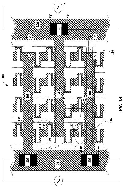
The shunt region (electric supply region) SH is a region for coupling the control gate electrode and the memory gate electrode that are formed integrally with (commonly to) the plural memory cells with the control gate line (selection gate line) and the memory gate line, and is disposed so as to be adjacent to the memory cell region 1 A. The control gate electrode and the memory gate electrode that extend to the memory cell region 1 A extend to the shunt region SH continuously. In the shunt region SH, the control gate electrode is coupled with the control gate line, and the memory gate electrode MG is coupled with the memory gate line.
The peripheral circuit 1 B is a circuit other than a non-volatile memory, and is a processor such as a CPU, control circuit, sense amplifier, column decoder, row decoder, and the like for example. The MISFET formed in the peripheral circuit 1 B is a MISFET for the peripheral circuit. In the present embodiment, a case of forming the n-channel type MISFET in the peripheral circuit region 1 B will be explained, however, it is also possible to reverse the electro-conductive type and to form a p-channel type MISFET in the peripheral circuit region 1 B, and it is also possible to form a CMISFET (Complementary MISFET) and the like in the peripheral circuit region 1 B.
As shown in FIG. 4 , first, the semiconductor substrate (semiconductor wafer) SB comprised of a p-type polycrystalline silicon and the like having the specific resistance of approximately 1-10 Ωcm for example is provided (Step S 1 of FIG. 1 ). Then, element separation regions (inter-element separating and insulating regions) ST that define an active region are formed over the main surface of the semiconductor substrate SB (Step S 2 of FIG. 1 ).
The element separation region ST is comprised of an insulating body such as silicon oxide, and can be formed by the STI (Shallow Trench Isolation) method or the LOCOS (Local Oxidization of Silicon) method and the like for example. The element separation region ST can be formed for example by forming a trench STR for separating the element in the main surface of the semiconductor substrate SB and thereafter embedding an insulating film comprised of silicon oxide for example in the inside of this trench STR for separating the element. More specifically, after forming the trench STR for separating the element in the main surface of the semiconductor substrate SB, an insulating film (silicon oxide film for example) for forming the element separation region is formed over the semiconductor substrate SB so as to embed this trench STR for separating the element therein. Then, by removing the insulating film outside the trench STR for separating the element (the insulating film for forming the element separation region), the element separation region ST comprised of the insulating film embedded in the trench STR for separating the element can be formed. The element separation region ST is disposed in the main surface of the semiconductor substrate SB so as to surround the active region where the element is formed. In other words, the elements are separated from each other by the element separation region ST. The element separation region ST electrically separates the memory cell region 1 A and the peripheral circuit region 1 B from each other, electrically separates the memory cells from each other in the memory cell region 1 A, and electrically separates the plural MISFETs from each other in the peripheral circuit region 1 B. In the shunt region SH, the element separation region ST having a large width is formed.
Next, as shown in FIG. 5 , a p-type well PW 1 is formed in the memory cell region 1 A of the semiconductor substrate SB, and a p-type well PW 2 is formed in the peripheral circuit region 1 B (Step S 3 of FIG. 1 ). The p-type wells PW 1 , PW 2 can be formed by ion injection and the like of the p-type impurities such as boron (B) for example into the semiconductor substrate SB. The p-type wells PW 1 , PW 2 are formed over a predetermined depth from the main surface of the semiconductor substrate SB. Because the p-type well PW 1 and the p-type well PW 2 have a same electro-conductive type, they may be formed in a same ion injection step or may be formed in a different ion injection step. Although it is not illustrated, the p-type well PW 1 of the memory cell region 1 A is covered with an n-type well in a plan view and a cross-sectional view, and is electrically separated from the p-type well PW 2 of the peripheral circuit region 1 B.
Next, after cleaning the surface of the semiconductor substrate SB (the p-type wells PW 1 , PW 2 ) by diluted hydrofluoric acid cleaning and the like, an insulating film GI for a gate insulating film is formed over the main surface of the semiconductor substrate SB (the surface of the p-type wells PW 1 , PW 2 ) (Step S 4 of FIG. 1 ).
The insulating film GI is formed of a thin silicon oxide film or an oxynitride silicon film and the like for example, and the forming film thickness of the insulating film GI can be made approximately 2-3 nm for example. The insulating film GI can be formed by the thermal oxidation method, the CVD (Chemical Vapor Deposition) method, or the plasma nitriding method. When the insulating film GI is formed by the thermal oxidation method, the insulating film GI is not formed over the element separation region ST.
As another aspect, in Step S 4 , it is also possible to form the insulating film GI of the peripheral circuit region 1 B with a different film thickness in a step other than the step for the insulating film GI of the memory cell region 1 A.
Next, as shown in FIG. 6 , a silicon film PS 1 is formed (laminated) over the main surface (entire surface of the main surface) of the semiconductor substrate SB namely over the insulating film GI of the memory cell region 1 A and the peripheral circuit region 1 B and over the element separation region ST of the shunt region SH (Step S 5 of FIG. 1 ).
The silicon film PS 1 is an electro-conductive film for forming a control gate electrode CG described below, and is an electro-conductive film for forming a first electrode D 1 described below which is formed integrally with the control gate electrode CG in the shunt region SH. Further, the silicon film PS 1 serves also as an electro-conductive film for forming a gate electrode DG described below. In other words, the control gate electrode CG described below, the gate electrode DG described below, and the first electrode D 1 described below are formed by the silicon film PS 1 .
The silicon film PS 1 is comprised of a polycrystalline silicon film (polysilicon film), and can be formed using the CVD method and the like. The laminated film thickness of the silicon film PS 1 can be made approximately 50-100 nm for example. The silicon film PS 1 can be made a semiconductor film of low resistance (doped polysilicon film) by introducing impurities at the time of film formation or by ion-injection of impurities after film formation. It is preferable that the silicon film PS 1 of the memory cell region 1 A and the shunt region SH is an n-type silicon film to which n-type impurities such as phosphor (P), arsenic (As) or the like has been introduced.
Next, an insulating film IL 1 is formed (laminated) over the main surface (entire surface of the main surface) of the semiconductor substrate SB namely over the silicon film PS 1 (Step S 6 of FIG. 1 ).
The insulating film IL 1 is an insulating film for forming cap insulating films CP 1 , CP 2 , CP 3 described below. The insulating film IL 1 is comprised of a silicon nitride film and the like for example, and can be formed using the CVD method and the like. The laminated film thickness of the insulating film IL 1 can be made approximately 20-50 nm for example. By executing Steps S 5 , S 6 , a state of forming a laminated film LF of the silicon film PS 1 and the insulating film IL 1 over the silicon film PS 1 comes up. Here, the laminated film LF is comprised of the silicon film PS 1 and the insulating film IL 1 over the silicon film PS 1 .
Next, the laminated film LF namely the insulating film IL 1 and the silicon film PS 1 is patterned by the photolithography technology and the etching technology, and a laminated body (laminated structure) LM 1 including the control gate electrode CG and the cap insulating film CP 1 over the control gate electrode CG is formed in the memory cell region 1 A (Step S 7 of FIG. 1 ).
Step S 7 can be executed as follows. That is to say, first, as shown in FIG. 6 , a photoresist pattern PR 1 is formed as a resist pattern over the insulating film IL 1 using the photolithography method. This photoresist pattern PR 1 is formed in a control gate electrode CG formation planned region in the memory cell region 1 A, the entire peripheral circuit region 1 B, and a first electrode D 1 formation planned region in the shunt region SH. Then, the laminated film LF of the silicon film PS 1 and the insulating film IL 1 in the memory cell region 1 A and the shunt region SH is patterned by etching (preferably by dry etching) using this photoresist pattern PR 1 as an etching mask, and this photoresist pattern PR 1 is thereafter removed. Thus, as shown in FIG. 7 , the laminated film LM 1 including the control gate electrode CG comprised of the silicon film PS 1 having been patterned and the cap insulating film CP 1 comprised of the insulating film IL 1 having been patterned is formed in the memory cell region 1 A. Also, a laminated body LM 2 including the first electrode D 1 comprised of the silicon film PS 1 having been patterned and the cap insulating film CP 2 comprised of the insulating film IL 1 having been patterned is formed in the shunt region SH.
The laminated body LM 1 is comprised of the control gate electrode CG and the cap insulating film CP 1 over the control gate electrode CG, and is formed over the semiconductor substrate SB (the p-type well PW 1 ) of the memory cell region 1 A through the insulating film GI. The control gate electrode CG and the cap insulating film CP 1 have plan shapes generally same to each other in a plan view, and overlap with each other in a plan view.
The laminated film LM 2 is comprised of the first electrode D 1 and the cap insulating film CP 2 over the first electrode, and is formed over the element separation region ST of the shunt region SH through the insulating film GI. In FIG. 8 and onward, the insulating film GI over the element separation region ST will be omitted. The first electrode D 1 and the cap insulating film CP 2 have plan shapes generally same to each other in a plan view, and overlap with each other in a plan view.
When Step S 7 is executed, the silicon film PS 1 and the insulating film IL 1 other than the portion that becomes the laminated body LM 1 are removed in the memory cell region 1 A, and the silicon film PS 1 and the insulating film IL 1 other than the portion that becomes the laminated body LM 2 are removed in the shunt region SH. On the other hand, in the peripheral circuit region 1 B, the photoresist pattern PR 1 is formed in the entire peripheral circuit region 1 B. Therefore, even when Step S 7 is executed, in the peripheral circuit region 1 B, the laminated film LF 1 comprised of the silicon film PS 1 and the insulating film IL 1 over the silicon film PS 1 remains as it is without being removed namely without being patterned. The laminated film LF remaining in the peripheral circuit region 1 B is marked with the reference sign LF 1 and is to be called the laminated film LF 1 .
In the memory cell region 1 A, the control gate electrode CG comprised of the patterned silicon film PS 1 is formed, and the control gate electrode CG is a gate electrode for the control transistor. The insulating film GI that remains below the control gate electrode CG becomes a gate insulating film of the control transistor. Therefore, in the memory cell region 1 A, the control gate electrode CG comprised of the silicon film PS 1 becomes a state of being formed over the semiconductor substrate SB (the p-type well PW 1 ) through the insulating film GI as the gate insulating film.
In the memory cell region 1 A, the insulating film GI other than the portion that is covered with the laminated body LM 1 namely the insulating film GI other than the portion that becomes the gate insulating film can possibly be removed by executing dry etching executed in the patterning step of Step S 7 or by executing wet etching after the dry etching.
Next, as shown in FIG. 8 , an insulating film MZ for a gate insulating film of a memory transistor is formed over the entire surface of the semiconductor substrate SB namely over the main surface (surface) of the semiconductor substrate SB and over the surface (the upper surfaces and the side surfaces) of the laminated bodies LM 1 , LM 2 (Step S 8 of FIG. 1 ).
In the peripheral circuit region 1 B, because the laminated film LF 1 remains, the insulating film MZ can possibly be formed over the surface (the upper surface and the side surface) of this laminated film LF 1 also. Therefore, in Step S 8 , the insulating film MZ is formed over the semiconductor substrate SB so as to cover the laminated body LM 1 of the memory cell region 1 A, the laminated body LM 2 of the shunt region SH, and the laminated film LF 1 of the peripheral circuit region 1 B.
The insulating film MZ is an insulating film for the gate insulating film of the memory transistor, and is an insulating film that includes an electric charge storage section in the inside thereof. This insulating film MZ is comprised of a laminated film of a silicon oxide film (oxide film) MZ 1 , a silicon nitride film (nitride film) MZ 2 formed over the silicon oxide film MZ 1 , and a silicon oxide film (oxide film) MZ 3 formed over the silicon nitride film MZ 2 . The laminated film of the silicon oxide film MZ 1 , the silicon nitride film MZ 2 , and the silicon oxide film MZ 3 can also be deemed to be an ONO (oxide-nitride-oxide) film.
Also, in order to make the drawing easy-to-use, in FIG. 8 , the insulating film MZ comprised of the silicon oxide film MZ 1 , the silicon nitride film MZ 2 , and the silicon oxide film MZ 3 is illustrated simply as the insulating film MZ. In the present embodiment, as an insulating film (electric charge storage layer) having the trap level, the silicon nitride film MZ 2 is exemplified, however, the insulating film is not limited to the silicon nitride film, and a high dielectric constant film having a higher dielectric constant compared to the silicon nitride film such as an aluminum oxide (alumina) film, a hafnium oxide film, or a tantalum oxide film for example can be also used as an electric charge storage layer or an electric charge storage section. Further, the electric charge storage layer or the electric charge storage section can be also formed of silicon nano-dots.
In order to form the insulating film MZ, for example, first, after forming the silicon oxide film MZ 1 by the thermal oxidation method (preferably ISSG oxidation), the silicon nitride film MZ 2 is laminated over the silicon oxide film MZ 1 by the CVD method, and the silicon oxide film MZ 3 is further formed over the silicon nitride film MZ 2 by the CVD method, or by the thermal oxidation method, or by both of them. Thus, the insulating film MZ comprised of the laminated film of the silicon oxide film MZ 1 , the silicon nitride film MZ 2 , and the silicon oxide film MZ 3 can be formed.
The thickness of the silicon oxide film MZ 1 can be made approximately 2-10 nm for example, the thickness of the silicon nitride film MZ 2 can be made approximately 5-15 nm for example, and the thickness of the silicon oxide film MZ 3 can be made approximately 2-10 nm for example. With respect to the last oxide film namely the silicon oxide film MZ 3 of the uppermost layer out of the insulating film MZ, a high withstanding voltage film can be formed also by oxidizing the upper layer portion of the nitride film (the silicon nitride film MZ 2 of the middle layer out of the insulating film MZ) for example. The insulating film MZ functions as a gate insulating film of a memory gate electrode MG formed later.
Next, a silicon film PS 2 is formed (laminated) as an electro-conductive film for forming the memory gate electrode MG over the main surface (entire surface of the main surface) of the semiconductor substrate SB namely over the insulating film MZ so as to cover the laminated bodies LM 1 , LM 2 in the memory cell region 1 A and the shunt region SH, and so as to cover the laminated film LF 1 in the peripheral circuit region 1 B (Step S 9 of FIG. 1 ).
The silicon film PS 2 is an electro-conductive film for a gate electrode of a memory transistor, and is an electro-conductive film for forming a second electrode D 2 described below which is formed integrally with the memory gate electrode MG in the shunt region SH. The silicon film PS 2 is comprised of a polycrystalline silicon film, and can be formed using the CVD method and the like. The laminated film thickness of the silicon film PS 2 can be made approximately 30-150 nm for example.
Also, the silicon film PS 2 is made a semiconductor film (doped polysilicon film) of low resistance by introducing impurities at the time of film formation or by introducing impurities by ion-injection of impurities after film formation. The silicon film PS 2 is an n-type silicon film to which n-type impurities such as phosphor (P), arsenic (As) or the like preferably has been introduced.
Next, the silicon film PS 2 is subjected to etching back (etching, anisotropic dry etching, anisotropic etching) by the anisotropic etching technology (Step S 10 of FIG. 1 ).
Because the silicon film PS 2 is subjected to etching back by the etch back step of Step S 10 , the silicon film PS 2 is made to remain in a side wall spacer shape over both of the side walls of the laminated body LM 1 through the insulating film MZ, and the silicon film PS 2 of the other region of the memory cell region 1 A is removed. Thus, as shown in FIG. 9 , in the memory cell region 1 A, the memory gate electrode MG is formed over one side wall out of both of the side walls of the laminated body LM 1 through the insulating film MZ by the silicon film PS 2 having remained in a side wall spacer shape, and a silicon spacer SP is formed over the other side wall by the silicon film PS 2 having remained in a side wall spacer shape through the insulating film MZ. The memory gate electrode MG is formed over the insulating film MZ so as to be adjacent to the laminated body LM 1 through the insulating film MZ. Because the laminated body LM 1 is comprised of the control gate electrode CG and the cap insulating film CP 1 over the control gate electrode CG, the memory gate electrode MG is formed over the insulating film MZ so as to be adjacent to the control gate electrode CG and the cap insulating film CP 1 through the insulating film MZ.
Also, in the shunt region SH, before the etch back step of Step S 10 , a photoresist pattern PR 2 is formed as a resist pattern (mask film) over the silicon film PS 2 using the photolithography method. This photoresist pattern PR 2 is formed in a second electrode D 2 formation planned region in the shunt region SH. Therefore, in the shunt region SH after the etch back step of Step S 10 , the second electrode D 2 is formed which covers a part of the upper surface and the side surface of the laminated body LM 2 through the insulating film MZ and extends over the element separation region ST. As shown in FIG. 9 , the second electrode D 2 has a reverse S-shape, and is comprised of a first section formed along the side wall of the first electrode D 1 , a second section formed over the element separation region ST and extending continuously from one end (lower end) of the first section in the direction of departing from the first electrode D 1 , and a third section extending over the first electrode D 1 from the other end (upper end) of the first section. Also, in the side wall of the laminated body LM 2 not covered by the second electrode D 2 , the silicon spacer SP is formed through the insulating film MZ.
Further, also over the side wall of the laminated film LF 1 that is made to remain in the peripheral circuit region 1 B, the silicon spacer SP is formed through the insulating film MZ.
The silicon spacer SP can be deemed also a side wall spacer comprised of an electric conductor namely an electric conductor spacer. In the memory cell region 1 A, the memory gate electrode MG and the silicon spacer SP are formed over the side walls of the laminated body LM 1 which become the opposite side from each other, and has a structure generally symmetric across the laminated body LM 1 .
At the stage the etch back step of Step S 10 has been completed, it is preferable that the height of the memory gate electrode MG and the silicon spacer SP is higher than the height of the control gate electrode CG. By making the height of the memory gate electrode MG higher than the height of the control gate electrode CG, in the polishing step of Step S 20 described below, the upper part of the memory gate electrode MG can be exposed accurately, and the exposure failure of the memory gate electrode MG can be prevented.
Next, after forming a photoresist pattern (not illustrated) of covering the memory gate electrode MG and exposing the silicon spacer SP over the semiconductor substrate SB using the photolithography technology, by dry etching using this photoresist pattern as the etching mask, the silicon spacer SP is removed (Step S 11 of FIG. 2 ). It is important that this photoresist pattern is a pattern that covers the second electrode D 2 in the shunt region SH. Thereafter, the photoresist pattern is removed. In the etching step of Step S 11 , as shown in FIG. 10 , although the silicon spacer SP is removed, the memory gate electrode MG remains without being etched because it has been covered by the photoresist pattern. Also, the silicon spacers SP of the side walls of the laminated bodies LM 2 , LF 1 are removed.
Next, as shown in FIG. 10 , out of the insulating film MZ, the portions that are not covered by the memory gate electrode MG or the second electrode D 2 and are exposed are removed by etching (wet etching for example) (Step S 12 of FIG. 2 ). At this time, in the memory cell region 1 A, the insulating film MZ positioned below the memory gate electrode MG and between the memory gate electrode MG and the laminated body LM 1 remains without being removed, and the insulating film MZ of the other region is removed. Also, in the shunt region SH, the insulating film MZ covered by the second electrode D 2 remains without being removed, and the insulating film MZ of the other region is removed. As it is known from FIG. 10 , in the memory cell region 1 A, the insulating film MZ extends continuously over both regions of the region between the memory gate electrode MG and the semiconductor substrate SB (the p-type well PW 1 ) and the region between the memory gate electrode MG and the laminated body LM 1 .
The insulating film MZ of the region between the memory gate electrode MG and the semiconductor substrate SB (the p-type well PW 1 ) functions as the gate insulating film of the memory transistor.
Next, by patterning the laminated film LF 1 of the peripheral circuit region 1 B using the photolithography technology and the etching technology, as shown in FIG. 11 , a laminated body (laminated structure) LM 3 including the gate electrode DG and the cap insulating film CP 3 over the gate electrode DG is formed in the peripheral circuit region 1 B (Step S 13 of FIG. 2 ).
The patterning step of Step S 13 can be executed as follows for example. That is to say, first, a photoresist pattern (not illustrated) is formed over the main surface of the semiconductor substrate SB using the photolithography method. This photoresist pattern is formed in the entire memory cell region 1 A, the entire shunt region SH, and a gate electrode DG formation planned region in the peripheral circuit region 1 B. Therefore, the memory gate electrode MG and the laminated body LM 1 as well as the first electrode D 1 and the second electrode D 2 come to be covered by this photoresist pattern. Then, using this photoresist pattern as the etching mask, the laminated film LF 1 of the silicon film PS 1 and the insulating film IL 1 in the peripheral circuit region 1 B is patterned by etching (preferably by dry etching), and this photoresist pattern is thereafter removed. Thus, as shown in FIG. 11 , the laminated body LM 3 of the gate electrode DG comprised of the patterned silicon film PS 1 and the cap insulating film CP 3 comprised of the patterned insulating film IL 1 is formed in the peripheral circuit region 1 B.
The description continues in the full USPTO document.
 Lapsed, fee not paid1 drawing