Background
The ultimate goal of three-dimensional display technology is to show a dynamic three-dimensional image. Despite the fact that the human visual system is uniquely constructed to function in a three-dimensional (3-D) world, the majority of current commercially available display technologies are based on flat, two-dimensional (2-D) methods of displaying visual information. In an attempt to display 3-D information on these displays, many sophisticated and powerful techniques, such as perspective, shadowing, and texturing have been developed to trick the eye into seeing a 3-D image. These techniques, however, are ultimately limited in effectiveness because they do not provide depth cues in a manner that is natural to visual processing. Therefore, displays capable of producing a true 3-D image are required to overcome the limitations of 2-D displays.
Volumetric displays form voxels—pixels in a 3-D grid—to represent objects in space. Because each voxel emits or scatters light at a specific point in space, volumetric displays represent objects having a more natural depth perception. Conventional 3-D volumetric displays utilize an upconversion process to produce an image within a volumetric display. One of the fundamental requirements for an upconversion volumetric 3-D display system is to have the entire display volume filled with voxels that can be selectively excited at any desired location. Methods of creating the required voxels include, solid-state (rare-earth particles doped into a glass host), gas medium (atomic vapor enclosed in a vaccum container), and crystal cube static screen (tiny dots engraved within a glass cube using a process known as Laser Subsurface Engraving), among others. To represent an object within the volume, two independently controlled laser beams activate a voxel only when they intersect in a process known as two-photon upconversion. Briefly, this process uses the energy of two infrared (IR) lasers to transform a material from a first level into a first excited level and then to a second excited level, from which it can make a visible fluorescence transition back to the first level. For this process to be useful as a display medium, each voxel must exhibit laser absorption from two different wavelengths, so that it is turned on only at the intersection of two independently scanned laser sources. Either laser by itself will not cause visible fluorescence. However, where both lasers are incident on the same voxel, two-step excitation results in fluorescence at the intersecting point. Scanning the intersection point fast enough, a flicker free 3-D image can be drawn in the volume. The eye cannot see changes faster than about 1.5 Hz. Therefore, if the image to be displayed is repeatedly drawn faster than this rate, the image will appear to be steady, even though visible light may be originating from any one point in the volume only a small fraction of the time.
Upconversion systems, however, are limited because these systems must write a new pattern at every discrete depth, requiring timing, processing, and control computations that limit the refresh rate, especially for large images, and require extensive electronic support systems. In addition, the brightness, color palette and contrast are primarily controlled by one or more high brightness, single-color laser sources or by a nonlinear optical process that produces a 3-D image from within the image space. Both methods restrict the range of colors in the image and increase the cost of the display, and the nonlinear process has difficulties in producing images bright enough to see in typical room illumination.
To overcome the rendering limitations of the above referenced volumetric displays, some systems have employed high quality 2-D images projected onto an opaque screen which was mechanically driven by a rotary or oscillating mechanism. The screen may have been rotated about an axis, or oscillated, for example, but the surface was always facing a fixed direction. As a result, the display would sweep a display space distributing frames of a 2-D image depending on the angle of the screen and the viewing angle. Different shapes of screens have been employed, including flat, helical, and thin elongated members such as a rod, beam, or stick. While these systems allowed full-color, high-contrast images to be produced, the refresh rate, size of the display, and viewing angle were limited by the mechanical nature of the system.
Some attempts to produce 3-D visual displays have also employed light emitting diodes (LEDs), for instance, on rotating blades. Like other systems, rotating LED systems have some desirable qualities, but, again, they have limitations that have kept them from being widely adopted to produce 3-D or holographic effects.
As a result of the above referenced limitations, there remains a need for systems and methods for easily producing bright, full-color, high-contrast 3-D images that are viewable continuously and equally over a wide range of viewing angles without the need for a mechanically driven opaque screen.
Brief description of the drawings
For a better understanding of the present disclosure, non-limiting and non-exhaustive embodiments are described in reference to the following drawings. In the drawings, like reference numerals refer to like parts through all the various figures unless otherwise specified.
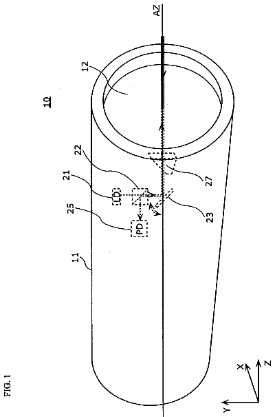
FIG. 1 is a schematic diagram of one exemplary embodiment of a three-dimensional display system providing a three-dimensional image within a volumetric image chamber.
FIG. 2 is a schematic diagram of one exemplary embodiment of the three-dimensional display system providing a diffusion screen at a predetermined location within the volumetric image chamber.
FIG. 3 is a schematic view of an exemplary control system for use in the three-dimensional display system illustrated in FIG. 1 .
FIG. 4 is a block flow diagram showing the operation of the three-dimensional display system shown in FIG. 1 .
FIG. 5 a -5 d are schematic views of exemplary image slice scanning patterns for forming the diffusion screen at predetermined locations within the volumetric image chamber.
FIG. 6 is a schematic diagram of another embodiment of the three-dimensional display system providing a diffusion screen within a thin-layer image chamber.
FIG. 7 is a top plan view showing an exemplary manner to generate 2-D images of multiple views of a 3D object in accordance with some embodiments disclosed herein.
Detailed description
The present inventive concepts will now be described more fully hereinafter with reference to the accompanying drawings, which form a part hereof, and which show, by way of illustration, specific exemplary embodiments by which the inventive concepts may be practiced. This inventive concepts may, however, be embodied in many different forms and should not be construed as limited to the embodiments set forth herein; rather, these embodiments are provided so that this disclosure will be thorough and complete, and will fully convey the scope of the inventive concepts to those skilled in the art. However, in some instances, well known or conventional details may not be described in order to not unnecessarily obscure the embodiments in detail. Among other things, the present inventive concepts may be embodied as methods or devices. Accordingly, the following detailed description is not to be taken in a limiting sense.
Reference throughout the specification to “at least some embodiments”, “another embodiment”, or “an embodiment” means that a particular feature, structure, or characteristic described in connection with the embodiment is included in at least some embodiments as described herein. Thus, the appearance of the phrases “in at least some embodiments” or “in an embodiment” in various places throughout the specification are not necessarily all referring to the same embodiment. Furthermore, the particular features, structures, or characteristics may be combined in any suitable manner in one or more embodiments.
Referring now to the figures, and in particular to FIGS. 1 and 2 , a three-dimensional display system 10 is schematically shown. FIG. 1 shows the three-dimensional display system 10 displaying a 3-D image 11 . FIG. 2 schematically shows an exemplary embodiment of the three-dimensional display system 10 having an addressing system 12 , an image writing/illumination system 14 , a single-frequency laser module 16 , an image chamber 18 , and a control system 20 . As shown in FIG. 1 , the 3-D image 11 is displayed within the image chamber 18 . As will be described in more detail below, in one embodiment, the 3-D image 11 is decomposed into a plurality of cross-sectional 2-D images at particular cross-sectional locations within the 3-D image 11 . Then, in a sequential process which steps through the cross-sectional locations, at each cross-sectional location, the three-dimensional display system 10
creates one or more diffusion screen within the image chamber 18 at the cross-sectional location,
supplies visible light in the form of the 2-D cross-sectional image onto the one or more diffusion screen to refract the visible light and provide views of the 2-D cross-sectional image at multiple different viewing angles around the image chamber 18 , and
erases the one or more diffusion screen.
The image chamber 18 is constructed of one or more materials that is/are configured to pass visible light and in which refractive indexes of particular and distinct locations within the material can be varied (e.g. set, stored and erased) in a predetermined manner to create and erase the diffusion screens. In one embodiment, the image chamber is constructed of a material having photo-refractive properties. The image chamber 18 can be constructed entirely or at least partially of a non-fluorescing, non-upconversion material. For example, the materials that may be used to make the image chamber 18 may include one or more particles that support a photorefractive process that converts spatial variations in optical intensity into spatial variations in the material's refractive index. Materials may include, but are not limited to, photothermoplatics, photorefractive crystals, photorefractive polymers, photoaddressable polymers, photopolymers, nanoparticle-based materials, microparticle-based materials, and glasses. Key parameters of interest for all of these materials include a time required to write a refractive index grating into particular locations within the material, the time required to erase the refractive index grating, the magnitude of the refractive index change, related to the contrast of the refractive index grating, caused by a given change in intensity, the optical clarity of the material (how much light is scattered by the material, even when no refractive index gratings are present), and the cost of the material. Several materials and their characteristics that can be used to make the image chamber 18 will be discussed below by way of non-limiting examples.
As discussed above, the image chamber 18 may be constructed of photorefractive crystals, e.g., certain bulk crystals that are configured to support the photorefractive effect that is desirable for use in the display. To cause the photorefractive effect, the crystals absorb light by trapped electrons allows the electrons to move freely and migrate through the crystal lattice where they are trapped again in adjacent unexposed regions. The spatially varying electric field that results from the variation in density of charged particles modulates the refractive index through the electro-optic effect. Inorganic ferroelectric crystals such as iron-doped lithium niobate (LiNbO3) and lithium tantalate (LiTaO3) have shown particular affinity for supporting efficient transfer of variations in intensity into changes in refractive index. Once a crystal material with the best combination of these properties is identified, the material is constructed as a solid crystal that is ideally homogeneous in its underlying crystalline structure. The bulk crystal can be grown using any number of commercially viable methods. In the ideal case a single uniform crystal is grown to the exact dimensions of the targeted image chamber. In other words, the image chamber 18 can ideally be a single uniform crystal. It is also possible that the image chamber 18 can be constructed by optically gluing several pieces of crystals to form a large size image chamber.
As another example, the image chamber 18 can be constructed of photorefractive polymers. In photoreactive polymers, the photorefractive effect arises in a similar manner to that of photorefractive crystals, except that the mobile charges are holes rather than electrons, and strong electric fields must be applied to support charge migration and enhance the electro-optic effects. Photorefractive polymers are amorphous materials, making them easier to mold into different and larger shapes that may be more conducive to use in certain applications.
As yet another example, the image chamber 18 can be constructed of photoaddressable polymers. Photoaddressable polymers consist of polymer materials that change their molecular configuration when exposed to light. This reaction to light is a local effect, meaning that the change in configuration occurs only at the site of exposure, and there is no requirement for diffusion on the molecular or electron level to create the change in the optical parameters of the material. By removing the need for diffusion, the potential exists for decreasing the write time of the material and improving contrast. Photoaddressable polymers primarily consist of azobenzene that contains liquid crystalline co-polymers. The azobenzene chromophores can exist in one of two isomeric states, i.e., a trans state and a cis state. In the trans state, the polymer molecules stretch into an elongated rod-like form. In the cis state, the molecule kinks and bends. Exposure to light of the correct wavelength can induce a change, called isomerization, from the cis state to the trans state and from the trans state to the cis state. The state of the material under equilibrium conditions depends only on the wavelength of the light and the temperature of the sample. Some materials that may be utilized for the main polymer chain include polyacrylates, polymethacrylates, polysiloxanes, polycarbonates, polyurethanes, polyimides, and aliphatic polyesters. Other advantages of the material include large, long-term stable changes in refractive index up to 0.5 which provide stable and high contrast refractive index modulation, an amorphous nature that allows simple processing and shaping, dry recording, and the ability to erase the refractive index changes that permits the writing and erasing of refractive index grating elements as needed.
As yet another example, the image chamber 18 can be constructed of photopolymers. Photopolymers are systems of organic molecules that function through the process of photoinitiation of polymerization to record volume diffractive elements to form refractive index gratings, as desired. These materials possess high light sensitivity, rapid writing time, and good stability of recorded variations, and are currently one of the most cost effective materials available for creating the image chamber 18 . A photopolymer system typically consists of one or more monomers, a photoinitiation system and a binder that is insensitive to light and does not contribute to the photopolymerization. The binder is, however, critical to the physical properties of the photopolymer, including rigidity and stability over long exposure to the environment. Common monomers used in these systems include acrylamide, dimethylacrylamide, 2-hydroxiethylmethacrylate, vinyl acetate, and acrylic acid, as these materials provide the material with high sensitivity, large dynamic range, and minimal shrinkage of the material upon exposure. The photoinitiation system may consists of a dye combined with an electron donor that are absorbing at the wavelength of the laser used to write the refractive index grating elements, which may also be described herein as “diffractive elements.” The absorbed energy is transferred in one of several ways to free radicals that can then initiate the polymerization reaction. Common photosensitive dyes include methylene blue, yellowish eosin, brillian green, and rose bengal. Common electron donors include triethanolamine, diethanolamine, ethanolamine, triethylamine, diethylamine, N-phenyl glycine, diphenyl iodonium choride, amongst others.
As yet another example, the image chamber 18 can be constructed of nanoparticle-based materials. Nanoparticle-based materials are a group of materials that are comprised of nanoparticles dispersed in a host material. Nanoparticles are structures that have dimensions on the order of tens of nanometers. Nanoparticles may consist of semiconductor structures, miniature crystals that may or may not contain dopant atoms, or similar material systems. For the image chamber 18 , the nanoparticles must be constructed of materials that display optical behaviors and responses that mimic that of the photorefractive materials. The nanoparticles may or may not be encapsulated in a coating layer. If the coating layer is present, it may contain active materials that contribute to the intended function of the nanoparticle or it may contain only passive materials that do not directly contribute to the nanoparticle's function. Once constructed, the nanoparticles may be dispersed in a host material by one of several common processes. The host material may be a liquid or a solid, and can include polymers, epoxies, and similar materials that are initially viscous and then subsequently solidify. This composite material may be used to fill the image chamber 18 and host the diffractive elements to be created.
As yet another example, the image chamber 18 can be constructed of microparticle-based materials. Microparticle-based materials are different from nanoparticle materials in that the microparticles are structures that have dimensions on the order of tens of micrometers rather than nanometers. Similarly to nanoparticles, microparticles may consist of semiconductor structures, miniature crystals that may or may not contain dopant atoms, or similar material systems. Microparticles can be obtained by controlled growth and manufacturing processes or by the grinding of bulk crystals of the material into micrometer size pieces. Microparticles are generally not encapsulated in a coating as the surface area is much smaller in proportion to the volume of the particle, and surface effects are of less concern. Once constructed, the microparticles may be dispersed in a host material by one of several common processes. The host material may be a liquid or a solid, and can include polymers, epoxies, and similar materials that are initially viscous and then subsequently solidify. This composite material may be used to fill the image chamber 18 .
Many of the important parameters for the microparticle-based materials are similar to those of the nanoparticle-based materials. Index matching, particle size, dopant choice and density, and host material properties are again concerns for the same reasons noted for the nanoparticle-based materials and will not be repeated here. An additional concern for microparticles is the uniformity of the particles in terms of volume and shape. For the method where microparticles are constructed by crushing and grinding of a bulk material, the uniformity of shape and size is typically very poor, and thus the grating recording efficiency, refractive index scattering and the optical clarity of the composite material may vary significantly throughout the material volume. This results in the creation of images with non-uniform intensity and contrast, which is undesirable. Microparticles formed by controlled growth have far less variability, but any variability will be more notable, since there will generally be a smaller number of particles present in the voxel volume and variability in the microparticle properties will be less likely to average out across the fewer particles. The larger particles are now on the same dimension of all of the optical wavelengths used in the three-dimensional display system 10 , so index matching may be more critical to avoid the diffraction effects that deteriorate the image quality.
Another possible material used for the image chamber 18 is a glass material doped with appropriate choices of ions that support the processes needed to induce stable variations in the optical properties of the glass to create, store and erase the diffusion screens at particular locations within the image chamber 18 . The glass material can be assembled or grown using any of several commercially viable methods. Glasses have the advantage of being amorphous materials that can be grown and shaped into image chambers of different dimensions and volumes and do not require precise crystalline assembly. The dimensions and volumes attainable for glasses are limited primarily by the equipment used to produce the glasses. Current processes for doping the glasses and physical constraints limit the maximum doping concentration that can be achieved. The limit on the number of dopant ions per unit volume limits the resolution and efficiency that can be achieved in each voxel of the three-dimensional image 11 .
As discussed above and shown in FIG. 2 , the three-dimensional display system 10 has the addressing system 12 , the image writing/illumination system 14 , the single frequency laser module 16 , the image chamber 18 , and the control system 20 . The single frequency laser module 16 is a laser which operates on a single resonator mode, so that the laser emits quasi-monochromatic radiation with a very small linewidth and low phase noise. The single frequency laser module 16 operates typically in the ultraviolet spectrum but may also operate in bands of the visible spectrum or infrared spectrum for which the image chamber 18 is reactive.
The addressing system 12 of the three-dimensional display system 10 may be provided with a scanning optical system 22 , at least one lens 24 , and may be configured to project a first directed optical energy 26 .
The image writing/illumination system 14 of the three-dimensional display system 10 may be provided having an image writing system 30 , an illumination system 32 , an optical combiner 34 , at least one lens 36 , and may be configured to project a second directed optical energy 38 . The three-dimensional display system 10 may further be provided with a connection 39 a , a connection 39 b , a connection 39 c , a first beam path 42 , a beam splitter 44 to provide an addressing beam 46 to a second beam path 48 , and a data beam 50 to a third beam path 52 .
The connection 39 a establishes communication between the control system 20 and the scanning optical system 22 to permit the control system 20 to supply information to and control the scanning optical system 22 as described below. The connection 39 b establishes communication between the control system 20 and the single-frequency laser module 16 to permit the control system 20 to selectively actuate and deactuate the single-frequency laser module 16 . The connection 39 c establishes communication between the control system 20 and the image writing system 30 and the illumination system 32 to permit the control system 20 to supply the 2-D pattern to the image writing system 30 and the 2-D image slices to the illumination system 32 and to control the image writing system 30 and the illumination system 32 .
The first beam path 42 connects an output port of the single-frequency laser module 16 to the beam splitter 44 so that an optical beam supplied by the single-frequency laser module 16 is provided to the beam splitter 44 . The beam splitter 44 splits the optical beam into the addressing beam 46 and the data beam 50 , preferably, such that the addressing beam 46 and the data beam 50 are coherent. The addressing beam 46 is supplied to the scanning optical system 22 via the second beam path 48 , and the data beam 50 is supplied to the image writing system 30 via the third beam path 52 . The first, second and third beam paths 42 , 48 and 52 may be fiber optic cables or free-space.
The addressing beam 46 is guided by the scanning optical system 22 and the lens 24 to form the first directed optical energy 26 . The first directed optical energy 26 is supplied into the image chamber 18 in the form of a plane that creates a voxel slice 60 . The voxel slice 60 is intersected by the second directed optical energy 38 generated from the image writing system 30 to create a diffusion screen 62 within the image chamber 18 . The addressing system 12 serves to specify the location of the diffusion screen 62 within the image chamber 18 by directing the voxel slice 60 to the desired location of the diffusion screen 62 . The image writing system 30 of the image writing/illumination system 14 receives the data beam 50 , which is in-coherence with the addressing beam 46 , and serves to specify the content or configuration of the diffusion screen 62 by creating the second directed optical energy 38 in a predetermined pixilated pattern. The diffusion screen 62 is set to refract the 2-D image slice in all horizontal, slanted, or vertical directions or a limited angle of view upon a desired field of view. Thus, in one embodiment, all of the diffusions screens 62 created in the image chamber 18 are identical. The diffusions screens 62 can be created so as to be spaced apart, and in particular locations corresponding to a location of the voxel slices 60 as shown in FIGS. 5A-5D , for example. Once the diffusion screen 62 is created, the illumination system 32 supplies visible light in the form of the 2-D image slice onto the diffusion screen 62 to create the 2-D image within the image chamber 18 .
The scanning optical system 22 , the image writing system 30 and the illumination system 32 may be constructed in a variety of manners, such as switch arrays having multiple rows and multiple columns which may be configured to direct light of different wavelengths that may be, in some instances projected in a visible spectrum, and in some instances in a spectrum not visible to the human eye. In one embodiment of the three-dimensional display system 10 , at least one of the scanning optical system 22 , the image writing system 30 and the illumination system 32 may be a digital micromirror device (DMD) as is known in the art. The DMD device may be built on a silicon wafer and consists of an array of small mirrors that are suspended above an air gap. The mirrors are suspended from flexible silicon frames that are free to flex when a voltage is applied to electrical connections attached to the frame. In a common construction of the DMD, the mirror is in one orientation when no voltage is applied, and the mirror rotates to a new position when a voltage is applied. Light energy incident on the mirror is therefore directed to a first output direction for no applied voltage and a second output direction when a voltage is applied. A voxel is selected or not selected by applying the correct voltage level to the mirror that corresponds to the voxel location within the voxel slice 60 . For example, an entire row or column of the mirrors in the switch array of the scanning optical system 22 can be selected, and all other rows or columns de-selected so as to project the first directed optical energy in the form of a plane at predetermined locations within the image chamber 18 . The 2-D pattern can be received and used by the image writing system 30 to create an interference pattern that will set the predetermined location within the image chamber 18 into the diffusion screen 62 . The 2-D pattern controls the characteristics of the diffusion screen 62 so that the visible light supplied by the illumination system 32 refracts into a desired field of view.
Light is then either directed toward the lens 24 or 36 and the image chamber 18 (voxel is illuminated) or directed away from the image chamber 18 (voxel is not illuminated). The DMD is commonly mounted on a printed circuit board that contains the circuitry, power supplies, microprocessors and other electronic systems for correctly driving the DMD. This electronics board is commonly referred to in the art as a digital light processing (DLP) board.
In another embodiment, one or more of the scanning optical system 22 , the image writing system 30 and the illumination system 32 may be a grating light valve (GLV) device built on a silicon wafer. In this example, the grating light valve in one or more of the scanning optical system 22 , the image writing system 30 and the illumination system 32 may have a plurality of switches with each switch having parallel rows of highly reflective micro-ribbons suspended above an air gap. The ribbons are a few μm in length and width and have a top layer of aluminum to make them reflective. The ribbons are configured to alternate between static ribbons which do not move and active ribbons that can be moved when a voltage is applied. Individual electrical connections to each ribbon electrode provide for independent movement. The ribbons and the substrate are electrically conductive. When the voltage of the active ribbons is set to ground potential, all ribbons are undeflected, and the switch acts as a standard mirror and directs light to one output direction. When a voltage is applied between the ribbon and base conductor the active ribbon deflects downward toward the substrate. This deflection creates diffraction effects on incident light causing the light to be reflected at a different angle than that of the undeflected ribbons. The wavelength to diffract is determined by the spatial frequency of the ribbons. As this spatial frequency is determined by the photolithographic mask used to form the GLV device in the CMOS fabrication process, the output angles can be very accurately controlled.
In still another embodiment, one or more of the scanning optical system 22 , the image writing system 30 and the illumination system 32 may be a liquid crystal display or LCD. The LCD consists of cells of liquid crystalline materials sandwiched between conductive plates. Polarizers are placed on the outside of both plates. The size of the cells is controlled by the process used to create the liquid crystal layer and to pattern the electrodes on the plates. Several different types of liquid crystalline materials can be used, all of which have the property that the orientation of the molecules within the material can be controlled by a voltage placed across the conductive plates. The polarization of the light traveling through each cell is affected by the orientation of the liquid crystal molecules and the polarizer on the input plate. In the most common configuration, when no voltage is applied the polarization of the light exiting the liquid crystal is such that all of the optical power is blocked by the polarizer on the output plate. When the correct voltage is applied across the plates, the polarization of the light exiting the liquid crystal is such that all of the optical power is passed by the output polarizer and thus this power can continue on to the lens 24 or 36 and illuminate the selected voxel. The LCD typically switches slower than the DMD and much slower than the GLV, and thus limits the speed at which successive 2-D slices of the 3-D image 11 can be addressed. The LCD is the most limiting of the switch arrays on the number of times the 3-D image 11 can be created per unit time, and therefore the image size will be most constrained. An advantage of the LCD approach is the ability to control the output optical power in an analog manner rather than the simple on-off function of the GLV and DMD. This provides the ability to control the intensity of the voxel emission at the switch array location rather than using an additional control system 20 .
In another embodiment of the three-dimensional display system 10 , the scanning optical system 22 and the image writing system 30 may be one type of switch array, for instance a DMD, configured to direct the addressing beam 46 and the data beam 50 into the image chamber 18 to create the diffusion screen 62 , and the illumination system 32 may be another type of switch array configured to direct visible light through the lens 36 to the image chamber 18 to create the 2-D image.
As shown in FIG. 2 , in one embodiment the image writing system 30 and the illumination system 32 supply light into the optical combiner 34 . The optical combiner 34 directs the light through the lens 36 and into the image chamber 18 . In such an embodiment, the optical combiner 34 allows the switches at the same location in each the image writing system 30 and the illumination system 32 to be responsible for directing light output to the same voxel in the voxel slice 60 within the image chamber 18 . The optical combiner 34 can be a prism. Other possible optical combiners, include but not limited to mirrors, and beam splitters that possess wavelength selective reflection and transmission properties. The light output from the image writing system 30 and the illumination system 32 pass through the optical combiner 34 and the image writing system 30 and the illumination system 32 are aligned such that outputs from the same switch location in the image writing system 30 and the illumination system 32 overlap at the optical combiner 34 . In this method, only a single lens system 36 is needed to direct the light from the image writing system 30 and the illumination system 32 to the voxel slice 60 . Other methods may be used, such as using a separate lens system for the image writing system 30 and the illumination system 32 .
The lenses 24 and 36 have several functions to perform. First, the lenses 24 and 36 transform the spacing of the switches in the scanning optical system 22 , the image writing system 30 and the illumination system 32 into the spacing of the voxels required in the voxel slice 60 . Second, the lenses 24 and 36 must ensure that all of the light from a given switch in the scanning optical system 22 , the image writing system 30 and the illumination system 32 is imaged to the targeted area of the voxel in the voxel slice 60 . Third, the lenses 24 and 36 must ensure that the shape of the first and second directed optical energy 26 and 38 wavefronts are of the appropriate shape to create the desired interference pattern within the voxel location in the image chamber 18 . Obtaining the correct shape of the wavefront is critical to obtaining the correct combination of diffraction surfaces in the diffraction screen 62 that will direct light from the illumination system 32 through a wide range of angles. A fourth potential function of the lenses 24 and 36 is to provide the means for implementing one of the different types of multiplexing that may be employed to create the required overlapping refractive index gratings.
Typically, a minimum of two lenses 24 and 36 are required for the three-dimensional display system 10 to perform each of these functions. In a high performance system, additional secondary lenses may be added to compensate for aberrations and distortions caused by the two lenses 24 and 36 . This compensation is designed such that the size of each voxel and the shape of the wavefront at the voxel are constant across the voxel slice 60 , and that all voxels are generated at the proper depth within the image chamber 18 .
Depending on the choice of the illumination system 32 , additional lens systems may be needed between the illumination system 32 and the optical combiner 34 . For example, if the illumination system 32 is a digital projector, where the switch array requires three switches, one for red, one for green, and one for blue, to compose one equivalent voxel in the image array, an additional lens system may be needed to combine the light beams from the three switches into a single light beam corresponding to one voxel in the voxel slice 60 and entering the optical combiner 34 at the correct location for each targeted voxel.
Another option for the lenses 24 and 36 is to use multiple arrays of lenses, with each lens in the array corresponding to one voxel in the voxel slice 60 . Such an arrangement would allow individual control of the first directed optical energy 26 and the second directed optical energy 38 for each voxel, if needed. This may be most important for a rotational slice approach (see FIG. 5 d ), where each column of the 3-D image 11 is potentially located at different depths in the image chamber 18 , and the voxels in each column may require different separations between the lenses 24 and 36 in order to achieve the same wavefront shape at each of these different depths.
For multiplexing purposes, several different implementations within the image writing/illumination system 14 may be used, depending in part on the choice of multiplexing employed [e.g., a particular type of multiplexing is described in Reference 1]. For shift multiplexing, one option is to shift the lens 36 relative to the optical combiner 34 and the image chamber 18 by small amounts. This can be accomplished if the lens 36 is designed such that shifting the lens 36 short distances away from its initial position simply shifts the location of the second directed optical energy 38 within the voxel but does not change the wavefront of the second directed optical energy 38 . Another method of shifting the second directed optical energy 38 location is a transparent plate or prism with parallel sides that can be rotated about one or more axes by small amounts. Phase coded multiplexing would require the placement of an SLM in the path of the second directed optical energy 38 to provide the required phase changes in the writing beam and/or erasing beams. The implementation of angular multiplexing will depend on the range of angles required as compared to the range of viewing angles that need to be achieved. For very small angles, the lens 36 may be designed such that shifting the lens 36 short distances away from its initial position causes both a shift in the position of the second directed optical energy 38 as it exits the lens 36 and an angular deflection of the second directed optical energy 38 from its original path. Increases in the shift distance increase the angular deflection of the second directed optical energy 38 . Larger angular deviations may require multiple image writing/illumination system 14 , one at each angle to be employed, a more sophisticated lens 36 design where the lenses within the overall system can be moved with respect to one another and the image writing system 30 and illumination system 32 , or placement of the entire image writing/illumination system 14 on the edge of a rotating plate or similar system in order to scan the image writing/illumination system 14 through the range of angles. Periostropic multiplexing is most easily achieved if the image space can be rotated. However, this approach is not practical in all possible implementations or applications of the three-dimensional display system 10 . Other options include the rotation of the image writing/illumination system 14 and the use of one or more rotating optical elements to effectively rotate the orientation of the output of the lens 36 .
The description continues in the full USPTO document.
 Lapsed, fee not paid6 drawings