Technical field
The present invention relates to a liquid crystal display device, and specifically to a liquid crystal display device for providing color display by four or more types of pixels for displaying different colors from each other.
Background art
Today, liquid crystal display devices are used in various applications. Each of pixels in a liquid crystal display device exhibits a luminance in accordance with the level of voltage applied to a liquid crystal layer. As an electrical representation, the pixel is represented as a liquid crystal capacitance formed by pixel electrode/liquid crystal layer/counter electrode. The level of voltage applied to the pixel (liquid crystal layer) is represented based on the potential of the counter electrode. A liquid crystal material is a dielectric material, and is deteriorated when being supplied with a DC voltage for a long period of time. In order to prevent this, the polarity (direction) of the voltage (electric field) applied to the liquid crystal layer is inverted at intervals of a certain time period (referred to as the “AC driving”). Frame inversion driving (or field inversion driving), by which the polarity of the voltage (direction of the electric field) applied to each pixel is inverted at intervals of a vertical scanning period is adopted.
However, in mass-produced liquid crystal display devices, it is difficult to accurately match the absolute values of the voltage before and after the polarity inversion of voltage. Each time the polarity is inverted, the absolute value of the voltage is slightly changed. As a result, while a still image is displayed, each time the polarity is inverted, the luminance is changed and thus the display flickers. According to a method for reducing the flicker, pixels supplied with voltages of opposite polarities are located to be adjacent to each other in a display area, so that the luminances of the pixels are spatially averaged. By use of this effect, the flicker is reduced. A representative technique of such a method is “one-dot inversion driving”, by which the polarities of the voltages applied to the adjacent pixels are made opposite to each other. The term “dot” means the pixel.
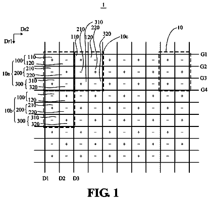
In a conventionally common liquid crystal display device, one color display includes three pixels for displaying red, green and blue, which are the three primary colors of light. The luminance of each pixel is controlled to provide color display. The color display pixel and the pixel may occasionally be referred to as the “pixel” and “sub pixel”, respectively (see, for example, Patent Document 1). When one-dot inversion driving is performed in a liquid crystal display device in which one color display pixel includes R, G and B pixels arrayed in a row direction, the polarities of the pixels in one row become R(+), G(−), B(+), R(−), G(+), B(−). Namely, when the polarities of the voltages applied to pixels adjacent to each other are made inverted to each other, the polarities of the voltages applied to pixels of a same color which are adjacent to each other are also made inverted to each other.
Recently, in order to enlarge the range of colors which can be displayed by a liquid crystal display device (referred to as the “color reproduction range”), techniques of using an increased number of primary colors for display have been proposed. For example, Patent Document 1 discloses a liquid crystal display device in which a color display pixel includes a red (R) pixel, a green (G) pixel, a blue (B) pixel, and a pixel of at least one more color (yellow (Y) pixel, a cyan (C) pixel, a magenta (M) pixel or a white (W) pixel). When the white pixel is used, the color reproduction range cannot be enlarged but the display luminance can be increased.
As shown in FIG. 8( a ) of Patent Document 1, when one-dot inversion driving is performed in a liquid crystal display device in which two color pixels are alternately arrayed in the row direction, the polarities of the pixels in one row become, for example, R(+), Y(−), R(+), Y(−). Namely, pixels of the same color are supplied with voltages of the same polarity. When display is provided with pixels of a particular color (e.g., when red is displayed in the entire screen), flicker occurs.
Patent Document 1 describes that flicker can be prevented by the following. A color display pixel includes four or more pixels, which include N pixels (N is an integer of 2 or greater) at least in a vertical scanning direction (column direction). Two-dot inversion driving (by which the polarity is inverted every second column of pixels) is performed in a horizontal scanning direction (row direction), and N horizontal line inversion driving (by which the polarity is inverted every N'th row of pixels) is performed in the vertical scanning direction.
Patent Document 2 also discloses a liquid crystal display device in which a color display pixel includes pixels arrayed in two rows by row columns, although this is not for the purpose of enlarging the color reproduction range (in Patent Document 2, the color display pixel is referred to as the “picture element”). As examples of combination of four pixels included in the color display pixel, Patent Document 2 shows a combination of one blue pixel, one red pixel and two green pixels, and a combination of one blue pixel, one red pixel, one green pixel and one white pixel. The liquid crystal display device disclosed in Patent Document 2 includes one scanning line common to the four pixels included in the color display pixel and four signal lines (two signal lines are provided in each of two positions sandwiching two pixels arrayed in the column direction). The polarities of the voltages supplied to adjacent signal lines are opposite to each other. Signal lines connected to pixels located at corresponding positions in color display pixels adjacent to each other in the row direction have different positional relationships from each other with respect to the corresponding pixels. As a result, the polarities of the signal voltages supplied to pixels of a same color which are adjacent to each other in the row direction are opposite to each other. Therefore, flicker can be prevented. CITATION LIST Patent Literature
Patent Document 1: Japanese Laid-Open Patent Publication No. 2008-76416
Patent Document 2: Japanese Laid-Open Patent Publication No. 2001-33757 SUMMARY OF INVENTION Technical Problem
Currently, liquid crystal display devices operable by double speed or quadruple speed driving and thus having improved moving image display characteristics have been put into practical use. More specifically, liquid crystal display devices in which the vertical scanning period is 1/120 sec. or 1/240 sec. have been developed, as opposed to a conventional liquid crystal display device in which the vertical scanning period is 1/60 sec. (vertical scanning frequency is 60 Hz). These newly developed liquid crystal display devices are for HDTV, and the display screen thereof has been progressively enlarged.
The “vertical scanning period” means a time period from when a scanning line (gate bus line) is selected until the same scanning line is selected the next time. In a conventional liquid crystal display device in which double speed driving is not performed, when the video signal is a signal for non-interlace driving, 1 vertical scanning period corresponds to 1 frame period of the video signal, whereas when the video signal is a signal for interlace driving, 1 vertical scanning period corresponds to 1 field of the video signal. For example, in the case of an NTSC signal, 1 vertical scanning period in a liquid crystal display device is 16.7 msec, which is the inverse of the field frequency of the NTSC signal (60 Hz). Since interlace driving is not performed in a liquid crystal display device, a signal voltage is written to all the pixels in both of an odd numbered field and an even numbered field. Therefore, the inverse of the field frequency of the NTSC signal is the vertical scanning period.
When dot inversion driving is performed in a liquid crystal display device including a great number of pixels, which is operable at 120 Hz or 240 Hz, for example, a liquid crystal display device for HDTV, the load on the signal line driving circuit (source driver) for supplying a signal voltage to the signal lines is increased. Namely, the power consumption by the signal line driving circuit is increased, and thus the caloric value is increased.
When the technology described in Patent Document 1 or 2 is adopted, flicker can be prevented in a liquid crystal display device in which the color display pixel includes four pixels arrayed in two rows by two columns as described above, but the load on the signal line driving circuit is large. In addition, when the vertical scanning frequency (also referred to simply as the “driving frequency”) is high, flicker is difficult to be visually recognized. From the point of view of industrial production, it is important that the load on the signal line driving circuit should be reduced.
The present invention made in light of the above-described problems has a main object of reducing the load on the signal line driving circuit in a liquid crystal display device in which a color display pixel includes four pixels arrayed in two rows by two columns. Solution to Problem
A liquid crystal display device according to the present invention includes a plurality of pixels arrayed in a matrix of a plurality of rows by a plurality of columns. The liquid crystal display device includes an active matrix substrate including a pixel electrode provided for each of the plurality of pixels, a switching element connected to the pixel electrode, a plurality of scanning lines extending in a row direction, and a plurality of signal lines extending in a column direction; a counter substrate facing the active matrix substrate; a liquid crystal layer provided between the active matrix substrate and the counter substrate; a scanning line driving circuit for supplying a scanning signal to each of the plurality of scanning lines; and a signal line driving circuit for supplying a positive or negative signal voltage to each of the plurality of signal lines. The plurality of pixels form a plurality of color display pixels, and the plurality of color display pixels each include first, second, third and fourth pixels arrayed in two rows by two columns; wherein the first pixel and the second pixel are adjacent to each other in the row direction, the third pixel and the fourth pixel are adjacent to each other in the row direction, the first pixel and the third pixel are adjacent to each other in the column direction, and the second pixel and the fourth pixel are adjacent to each other in the column direction. The plurality of signal lines include first and second signal lines which are located in correspondence with each column of pixels and are supplied with signal voltages of opposite polarities from each other from the signal line driving circuit in each vertical scanning period. In an arbitrary color display pixel, the switching element of one of the first and third pixels is connected to the first signal line, the switching element of the other of the first and third pixels is connected to the second signal line, the switching element of one of the second and fourth pixels is connected to the first signal line, the switching element of the other of the second and fourth pixels is connected to the second signal line, and the switching elements of the first, second, third and fourth pixels are controlled to be ON/OFF by a common scanning signal. During an arbitrary vertical scanning period, the polarities of the signal voltages supplied to the first and second signal lines are constant. The polarities of the signal voltages supplied to the first and second signal lines are inverted at intervals of a vertical scanning period or at intervals of two or more vertical scanning periods. The color display pixel may include pixels in 2 rows by an even number of columns.
In an embodiment, in a color display pixel adjacent to the arbitrary color display pixel in the column direction, the switching element of one of the first and third pixels is connected to the second signal line, the switching element of the other of the first and third pixels is connected to the first signal line, the switching element of one of the second and fourth pixels is connected to the second signal line, and the switching element of the other of the second and fourth pixels is connected to the first signal line.
In an embodiment, in an arbitrary vertical scanning period, a polarity of the signal voltage supplied to each of the first, second, third and fourth pixels included in an arbitrary color display pixel, and a polarity of the signal voltage supplied to each of the first, second, third and fourth pixels included in a color display pixel adjacent to the arbitrary color display pixel in the row direction, are opposite to each other.
In an embodiment, in an arbitrary vertical scanning period, the polarities of the voltage signals supplied to the first pixel and the second pixel included in an arbitrary first color display pixel are opposite to each other, and the polarities of the voltage signals supplied to the third pixel and the fourth pixel included in the arbitrary first color display pixel are opposite to each other.
In an embodiment, in an arbitrary vertical scanning period, the polarities of the signal voltages supplied to two arbitrary signal lines adjacent to each other, among the plurality of signals, are opposite to each other.
In an embodiment, in an arbitrary color display pixel, the switching elements of the first, second, third and fourth pixels are connected to a common scanning line.
In an embodiment, the first, second, third and fourth pixels include one of a yellow pixel, a cyan pixel, a magenta pixel and a white pixel in addition to a red pixel, a blue pixel and a green pixel.
In an embodiment, for displaying an intermediate gray scale level, the plurality of pixels each include a bright sub pixel exhibiting a luminance higher than that of the gray scale level to be displayed and a dark sub pixel exhibiting a luminance lower than that of the gray scale level to be displayed.
In an embodiment, the vertical scanning period is 1/120 seconds or shorter.
A liquid crystal display device in an embodiment is of a VA mode, for example, of a PSA mode. Advantageous Effects of Invention
According to the present invention, in a liquid crystal display device in which a color display pixel includes four pixels arrayed in two rows by two columns, the load on the signal line driving circuit can be reduced.
Brief description of drawings
FIG. 1( a ) is a schematic plan view of a liquid crystal display device 100 in an embodiment according to the present invention; and FIG. 1( b ) is a schematic view showing electrical connections regarding pixels in a liquid crystal display panel 10 .
FIG. 2 shows connections between TFTs 14 of four pixels P.sub.1 through P.sub.4 and two signal lines 13 , and a polarity distribution of signal voltages supplied to the pixels, in a liquid crystal display panel 10 A.
FIG. 3 shows connections between TFTs 14 of four pixels P.sub.1 through P.sub.4 and two signal lines 13 , and a polarity distribution of signal voltages supplied to the pixels, in a liquid crystal display panel 10 B.
FIG. 4 shows connections between TFTs 14 of four pixels P.sub.1 through P.sub.4 and two signal lines 13 , and a polarity distribution of signal voltages supplied to the pixels, in a liquid crystal display panel 10 C.
FIG. 5 shows connections between TFTs 14 of four pixels P.sub.1 through P.sub.4 and two signal lines 13 , and a polarity distribution of signal voltages supplied to the pixels, in a liquid crystal display panel 10 D.
FIG. 6 shows connections between TFTs of pixels and signal lines, and gate signals, in a liquid crystal display panel 10 E having a multi-pixel structure.
FIG. 7 shows an equivalent circuit of three pixels (three pixels enclosed by the one-dot chain line in FIG. 6 ) in the liquid crystal display panel 10 E.
FIG. 8 is a schematic plan view of a pixel electrode 11 A usable for a PSA mode liquid crystal display device in an embodiment according to the present invention.
Description of embodiments
Hereinafter, liquid crystal display devices in embodiments according to the present invention will be described with reference to the drawings. The present invention is not limited to the following embodiments provided as examples.
With reference to FIGS. 1( a ) and ( b ) , a structure of a liquid crystal display device 100 in an embodiment according to the present invention will be described. FIG. 1( a ) is a schematic plan view of the liquid crystal display device 100 , and FIG. 1( b ) is a schematic view showing electrical connections regarding pixels in a liquid crystal display panel 10 .
As shown in FIG. 1( a ) , the liquid crystal display device 100 includes the liquid crystal display panel 10 including a plurality of pixels P arrayed in a matrix of a plurality of rows by a plurality of columns, and a scanning line driving circuit (gate driver) 20 and a signal line driving circuit (source driver) 30 both for supplying driving signals to the liquid crystal display panel 10 .
The plurality of pixels P in the liquid crystal display panel 10 form a plurality of color display pixels P.sub.CD, and each of the color display pixels P.sub.CD includes four pixels P. The four pixels P are a first pixel P.sub.1, a second pixel P.sub.2, a third pixel P.sub.3 and a fourth pixel P.sub.4 which are arrayed in two rows by two columns. The first pixel P.sub.1 and the second pixel P.sub.2 are adjacent to each other in a row direction, and the third pixel P.sub.3 and the fourth pixel P.sub.4 are adjacent to each other in the row direction. The first pixel P.sub.1 and the third pixel P.sub.3 are adjacent to each other in a column direction, and the second pixel P.sub.2 and the fourth pixel P.sub.4 are adjacent to each other in the column direction.
In this example, the first pixel P.sub.1 is a red (R) pixel, the second pixel P.sub.2 is a yellow (R) pixel, the third pixel P.sub.3 is a blue (B) pixel, and the fourth pixel P.sub.4 is a green (G) pixel. FIG. 1( a ) shows one row and one column of the color display pixels and omits the other color display pixels. The same color display pixels as those shown in the figure are arrayed in a matrix. The colors of the four pixels P.sub.1 through P.sub.4 included in the color display pixel are not limited to the above. From the point of view of color reproducibility, it is preferable that at least R, G and B pixels are included. Preferably, the other color is yellow (Y), cyan (C) or magenta (M), but may be white (W).
It is not necessary that the four pixels P.sub.1 through P.sub.4 all have the same size. From the point of view of color reproducibility, it is preferable that the red pixel and the blue pixel are larger than the pixels of the other two colors. In order to provide the scanning lines and the signal lines linearly, it is preferable that each pixel is generally rectangular, that the first pixel P.sub.1 and the second pixel P.sub.2 arrayed in the row direction have an equal length in the column direction, that the third pixel P.sub.3 and the fourth second pixel P.sub.4 arrayed in the row direction have an equal length in the column direction, that the first pixel P.sub.1 and the third pixel P.sub.3 arrayed in the column direction have an equal length (width) in the row direction, and that the second pixel P.sub.2 and the fourth pixel P.sub.4 arrayed in the column direction have an equal length (width) in the row direction. Preferably, the color display pixel P.sub.CD is generally square.
Now, with reference to FIG. 1( b ) , electrical connections regarding a pixel in the liquid crystal display panel 10 will be described. FIG. 1( b ) is a plan view of an active matrix substrate (TFT substrate) 10 a included in the liquid crystal display panel 10 , but omits a liquid crystal layer and a counter substrate located to face the active matrix substrate 10 a with the liquid crystal layer being held therebetween. The counter substrate typically includes a counter electrode, a color filter layer, a light blocking layer (black matrix), and the like. The color filter layer may be provided in the active matrix substrate. As is well known, in a liquid crystal display device of an IPS mode or an FFS mode, the counter electrode may be provided in the active matrix substrate.
FIG. 1( b ) shows an area of the active matrix substrate 10 a which corresponds to four pixels included in one color display pixel P.sub.CD.
As shown in FIG. 1( b ) , the active matrix substrate 10 a includes a pixel electrode 11 provided for each of the pixels P, a switching element (in this example, TFT) 14 connected to the pixel electrode 11 , a plurality of scanning lines (gate bus lines) 12 extending in the row direction, and a plurality of signal lines (source bus lines) 13 extending in the column direction. The scanning line driving circuit 20 shown in FIG. 1( a ) supplies a scanning signal to each of the plurality of scanning lines 12 , and the signal line driving circuit 30 shown in FIG. 1( a ) supplies a positive or negative signal voltage to each of the plurality of signal lines 13 . Herein, a TFT type liquid crystal display device including the TFT 14 as a switching element will be described, but the switching element may be anything which operates in substantially the same manner as the TFT 14 .
The plurality of signal lines 13 include a first signal line 13 a and a second signal line 13 b which are provided in correspondence with each column of pixels. The first signal line 13 a and the second signal line 13 b are supplied with signal voltages of opposite polarities from each other from the signal line driving circuit 30 in each vertical scanning period. For example, while the first signal line 13 a is supplied with a positive signal voltage, the second signal line 13 b is supplied with a negative signal voltage. Herein, among the two signal lines 13 a and 13 b located in correspondence with each column of pixels, the left signal line is referred to as the “first signal line 13 a ” and the right signal line is referred to as the “second signal line 13 b ”. The polarities of the signal voltages supplied to the first signal line 13 a and the second signal line 13 b are independent in each column of pixels. Specifically, referring to FIG. 1( b ) , the polarity of the signal voltage supplied to a first signal line S.sub.a(n) located in correspondence with an n'th column of pixels, and the polarity of the signal voltage supplied to a first signal line S.sub.a(n+1) located in correspondence with the (n+1)th column of pixels, are independent from each other. Similarly, the polarity of the signal voltage supplied to a second signal line S.sub.b(n) located in correspondence with the n'th column of pixels, and the polarity of the signal voltage supplied to a second signal line S.sub.b(n+1) located in correspondence with the (n+1)th column of pixels, are independent from each other. In the above, the polarity of the signal voltage supplied to the first signal line S.sub.a(n) and the polarity of the signal voltage supplied to the second signal line S.sub.b(n) are opposite to each other. The polarity of the signal voltage supplied to the first signal line S.sub.a(n+1) and the polarity of the signal voltage supplied to the second signal line S.sub.b(n+1) are opposite to each other.
In an arbitrary color display pixel P.sub.CD, the TFT 14 of one of the first pixel P.sub.1 and the third pixel P.sub.3 is connected to the first signal line 13 a , and the TFT 14 of the other of the first pixel P.sub.1 and the third pixel P.sub.3 is connected to the second signal line 13 b . The TFT 14 of one of the second pixel P.sub.2 and the fourth pixel P.sub.4 is connected to the first signal line 13 a , and the TFT 14 of the other of the second pixel P.sub.2 and the fourth pixel P.sub.4 is connected to the second signal line 13 b . In this example, the TFT 14 of the first pixel P.sub.1 is connected to the first signal line 13 a , and the TFT 14 of the third pixel P.sub.3 is connected to the second signal line 13 b . The TFT 14 of the third pixel P.sub.3 is connected to the second signal line 13 b , and the TFT 14 of the fourth pixel P.sub.4 is connected to the first signal line 13 a . The TFTs may each be connected to the opposite signal line.
The TFTs 14 of the four pixels P.sub.1 through P.sub.4 are all controlled to be ON/OFF by a common scanning signal. In this example, the TFTs 14 of the four pixels P.sub.1 through P.sub.4 are all connected to a common scanning line 12 . Alternatively, as long as the TFTs 14 are controlled to be ON/OFF by a common scanning signal, the scanning signal may be supplied from different scanning lines. For example, as described later, in the case where one pixel electrode includes two sub pixel electrodes, specifically, a bright sub pixel exhibiting a luminance higher than that of the gray scale level to be displayed and a dark sub pixel exhibiting a luminance lower than that of the gray scale level to be displayed, two scanning lines are provided in correspondence with the two sub pixel electrodes and a common scanning signal is supplied to the scanning lines.
With such a structure, the four pixels P.sub.1 through P.sub.4 included in one color display pixel P.sub.CD are driven by one scanning line G.sub.(m), and four signal lines S.sub.a(n), S.sub.b(n), S.sub.a(n+1) and S.sub.b(n+1). As a result, although the number of rows of pixels is larger (twice) than that in a conventional stripe-array structure (in which four color pixels are provided in each row, and pixels of one of the colors are provided in each column), the time required for supplying a signal voltage to each pixel (time period in which the TFT 14 is in an ON state; also referred to as the “write time”) can be the same as in the conventional stripe-array structure. Accordingly, there is no obstacle against double speed or quadruple speed driving performed on the scanning and signal lines.
In addition, the polarity of the voltage applied to the first pixel P.sub.1 and the polarity of the voltage applied to the third pixel P.sub.3 are opposite to each other, and the polarity of the voltage applied to the second pixel P.sub.2 and the polarity of the voltage applied to the fourth pixel P.sub.4 are opposite to each other. Therefore, among two among the four pixels P.sub.1 through P.sub.4 included in each color display pixel P.sub.CD, two pixels are supplied with a positive voltage, and the other two pixels are supplied with a negative voltage.
In the liquid crystal display device 100 in an embodiment according to the present invention, during an arbitrary vertical scanning period, the polarities of the signal voltages supplied to the first signal line 13 a and the second signal line 13 b are constant. Needless to say, in the liquid crystal display device 100 , AC driving is performed and therefore the polarities of the signal voltages supplied to the first signal line 13 a and the second signal line 13 b are inverted at intervals of a vertical scanning period. Namely, the signal line driving circuit 30 merely inverts the polarity of the signal voltage supplied to each signal line 13 at intervals of a vertical scanning period, regardless of the number of rows of pixels (i.e., the cycle of polarity inversion is twice the vertical scanning period). Therefore, the load on the signal line driving circuit 30 of the liquid crystal display device 100 is smaller than the load on the signal line driving circuit in the liquid crystal display devices described in Patent Documents 1 and 2 or a conventionally common stripe array type liquid crystal display device. In this example, the polarity of the signal voltage supplied to each signal line 13 is inverted at intervals of a vertical scanning period. Alternatively, the polarity of the signal voltage supplied to each signal line 13 may be inverted at intervals of two or more vertical scanning periods. For example, when one, same image is written with the same polarity for two vertical scanning periods during driving at 240 Hz, there is an advantage that a sufficient time for charging the pixel can be obtained. As the cycle of polarity inversion is longer, the power consumption is smaller.
The above-described advantage of the liquid crystal display device 100 is conspicuous when double speed or quadruple speed driving is performed, namely, when the vertical scanning period is 1/120 sec. or less. Even when the conventional 60 Hz driving is performed, there is an advantage that the power consumption can be reduced. Therefore, as described in Patent Documents 1 and 2, it is preferable that the liquid crystal display device is structured so as to prevent flicker. Hereinafter, with reference to FIG. 2 through FIG. 5 , a structure for preventing flicker will be described.
FIG. 2 through FIG. 5 show the connections between the TFTs 14 of the four pixels P.sub.1 through P.sub.4 and the two signal lines 13 , and a polarity distribution of the signal voltages applied to the pixels, in liquid crystal display panels 10 A through 10 D usable as the liquid crystal display panel 10 of the liquid crystal display device 100 .
The liquid crystal display panels 10 A through 10 D shown in FIG. 2 through FIG. 5 each have the structure of the liquid crystal display panel 10 described above with reference to FIG. 1 . The polarity of the signal voltage supplied to each signal line 13 is not changed during the vertical scanning period and is inverted at intervals of a vertical scanning period. FIG. 2 through FIG. 5 show the polarities of the signal voltages applied to the pixels in a certain vertical scanning period. At the next vertical scanning period, the polarities of the signal voltages applied to the pixels are all inverted.
In the liquid crystal display panels 10 A and 10 B shown in FIG. 2 and FIG. 3 , among the four signal lines S.sub.a(n), S.sub.b(n), S.sub.a(n+1) and S.sub.b(n+1), the signal lines S.sub.a(n) and S.sub.a(n+1) are of the same polarity (in this example, positive), and the signal lines S.sub.b(n) and S.sub.b(n+1) are of the same polarity (in this example, negative). By contrast, in the liquid crystal display panels 10 C and 10 D shown in FIG. 4 and FIG. 5 , among the four signal lines S.sub.a(n), S.sub.b(n), S.sub.a(n+1) and S.sub.b(n+1), the signal lines S.sub.a(n) and S.sub.b(n+1) are of the same polarity (in this example, positive), and the signal lines S.sub.b(n) and S.sub.a(n+1) are of the same polarity (in this example, negative).
As shown in FIG. 2 and FIG. 3 , when the polarities of the signal voltages supplied to arbitrary two signal lines adjacent to each other are opposite to each other, the following advantages are obtained. For example, it is now assumed that there is a small foreign object on the signal lines and a small leak current is generated between the two signal lines (e.g., S.sub.b(n) and S.sub.a(n+1)) via the foreign object. In this case, when the polarities of the voltages supplied to the signal lines close to each other are opposite to each other, a relatively high voltage is applied between these signal lines. As a result, a relatively large current flows in the foreign object. When this occurs, the foreign object is destroyed by the Joule heat, and as a result, the leak defect may be repaired. In addition, when the polarities of the signal voltages supplied to signal lines adjacent to each other are opposite to each other, the signal line driving circuit for dot inversion driving of a conventional liquid crystal display device having a stripe array of R, G and B pixels can be used as it is.
Regarding the liquid crystal display panel 10 A shown in FIG. 2 , in the color display pixel P.sub.CD including the first pixel P.sub.1 of an m'th row and the n'th column, the TFT 14 of the first pixel P.sub.1 is connected to the first signal line S.sub.a(n), and the TFT 14 of the third pixel P.sub.3 is connected to the second signal line S.sub.b(n). The TFT 14 of the second pixel P.sub.2 is connected to the second signal line S.sub.b(n+1), and the TFT 14 of the fourth pixel P.sub.4 is connected to the first signal line S.sub.a(n+1). Accordingly, regarding the polarities of the signal voltages supplied to the four pixels P.sub.1 through P.sub.4, the polarities of the signal voltages supplied to the first pixel P.sub.1 and the second pixel P.sub.2 are opposite to each other, and the polarities of the signal voltages supplied to the third pixel P.sub.3 and the fourth pixel P.sub.4 are opposite to each other.
Next, the color display pixel P.sub.CD including the first pixel P.sub.1 of the (m+1)th row and the n'th column will be described. In this color display pixel, the TFT 14 of the first pixel P.sub.1 is connected to the second signal line S.sub.b(n), and the TFT 14 of the third pixel P.sub.3 is connected to the first signal line S.sub.a(n). The TFT 14 of the second pixel P.sub.2 is connected to the first signal line S.sub.a(n+1), and the TFT 14 of the fourth pixel P.sub.4 is connected to the second signal line S.sub.b(n+1).
Namely, in one of two color display pixels adjacent to each other in the column direction, the connection relationship between the TFTs 14 of the four pixels P.sub.1 through P.sub.4 and the two signal lines 13 (e.g., signal lines S.sub.a(n) and S.sub.b(n), and signal lines S.sub.a(n+1) and S.sub.b(n+1)) is opposite to that in the other of the two color display pixels. As a result, the polarities of the voltages applied to the pixels of a same color which are adjacent to each other in the column direction are opposite to each other. For example, the first pixel P.sub.1 of the m'th row and the n'th column is supplied with a positive voltage, and the first pixel P.sub.1 of the (m+1)th row and the n'th column is supplied with a negative voltage. Regarding the second through fourth pixels also, the polarities of the voltages applied to the pixels of a same color which are adjacent to each other in the column direction are opposite to each other.
Next, the color display pixel P.sub.CD including the first pixel P.sub.1 of the m'th row and the (n+2)th column will be described. In this color display pixel, the TFT 14 of the first pixel P.sub.1 is connected to the second signal line S.sub.b(n+2), and the TFT 14 of the third pixel P.sub.3 is connected to the first signal line S.sub.a(n+2). The TFT 14 of the second pixel P.sub.2 is connected to the first signal line S.sub.a(n+3), and the TFT 14 of the fourth pixel P.sub.4 is connected to the second signal line S.sub.b(n+3).
Namely, in one of two color display pixels adjacent to each other in the row direction, the connection relationship between the TFTs 14 of the four pixels P.sub.1 through P.sub.4 and the two signal lines 13 (e.g., signal lines S.sub.a(n) and S.sub.b(n), and signal lines S.sub.a(n+2) and S.sub.b(n+2)) is opposite to that in the other of the two color display pixels. As a result, the polarities of the voltages applied to the pixels of a same color which are adjacent to each other in the row direction are opposite to each other. For example, the first pixel P.sub.1 of the m'th row and the n'th column is supplied with a positive voltage, and the first pixel P.sub.1 of the m'th row and the (n+2)th column is supplied with a negative voltage. Regarding the second through fourth pixels also, the polarities of the voltages applied to the pixels of a same color which are adjacent to each other in the row direction are opposite to each other.
As can be seen from FIG. 2 , the polarity of the voltage applied to the first pixel P.sub.1 (hatched) in one color display pixel is opposite to that in a color display pixel adjacent to the one color display pixel in the column direction, and is opposite to that in a color display pixel adjacent to the one color display pixel in the row direction. The second through fourth pixels also have this relationship. Accordingly, the liquid crystal display panel 10 A can prevent flicker as the liquid crystal display devices described in Patent Documents 1 and 2.
Now, FIG. 3 will be referred to. Regarding the liquid crystal display panel 10 B shown in FIG. 3 , in the color display pixel P.sub.CD including the first pixel P.sub.1 of the m'th row and the n'th column, the TFT 14 of the first pixel P.sub.1 is connected to the first signal line S.sub.a(n), and the TFT 14 of the third pixel P.sub.3 is connected to the second signal line S.sub.b(n). The TFT 14 of the second pixel P.sub.2 is connected to the first signal line S.sub.a(n+1), and the TFT 14 of the fourth pixel P.sub.4 is connected to the second signal line S.sub.b(n+1). The connection relationship between the TFTs 14 and the two signal lines S.sub.a(n+1) and S.sub.b(n+1) regarding the second pixel P.sub.2 and the fourth pixel P.sub.4 is opposite to that of the liquid crystal display panel 10 A shown in FIG. 2 . Accordingly, regarding the polarities of the signal voltages supplied to the four pixels P.sub.1 through P.sub.4, the polarities of the signal voltages supplied to the first pixel P.sub.1 and the second pixel P.sub.2 are the same as each other, and the polarities of the signal voltages supplied to the third pixel P.sub.3 and the fourth pixel P.sub.4 are the same as each other.
Next, the color display pixel P.sub.CD including the first pixel P.sub.1 of the (m+1)th row and the n'th column will be described. In this color display pixel, the TFT 14 of the first pixel P.sub.1 is connected to the second signal line S.sub.b(n), and the TFT 14 of the third pixel P.sub.3 is connected to the first signal line S.sub.a(n). The TFT 14 of the second pixel P.sub.2 is connected to the second signal line S.sub.b(n+1), and the TFT 14 of the fourth pixel P.sub.4 is connected to the first signal line S.sub.a(n+1).
Namely, in one of two color display pixels adjacent to each other in the column direction, the connection relationship between the TFTs 14 of the four pixels P.sub.1 through P.sub.4 and the two signal lines 13 (e.g., signal lines S.sub.a(n) and S.sub.b(n), and signal lines S.sub.a(n+1) and S.sub.b(n+1)) is opposite to that in the other of the two color display pixels. As a result, the polarities of the voltages applied to the pixels of a same color which are adjacent to each other in the column direction are opposite to each other. For example, the first pixel P.sub.1 of the m'th row and the n'th column is supplied with a positive voltage, and the first pixel P.sub.1 of the (m+1)th row and the n'th column is supplied with a negative voltage. Regarding the second through fourth pixels also, the polarities of the voltages applied to the pixels of a same color which are adjacent to each other in the column direction are opposite to each other.
Next, the color display pixel P.sub.CD including the first pixel P.sub.1 of the m'th row and the (n+2)th column will be described. In this color display pixel, the TFT 14 of the first pixel P.sub.1 is connected to the second signal line S.sub.b(n+2), and the TFT 14 of the third pixel P.sub.3 is connected to the first signal line S.sub.a(n+2). The TFT 14 of the second pixel P.sub.2 is connected to the second signal line S.sub.b(n+3), and the TFT 14 of the fourth pixel P.sub.4 is connected to the first signal line S.sub.a(n+3).
The description continues in the full USPTO document.
 Lapsed, fee not paid8 drawings