Lapsed, fee not paid6 drawings
Cameras, Displays & Optics · US 9,817,298 B1
Camera with aerodynamic housing
A camera includes a primary housing that has a cylindrical exterior surface and an opening located at a front end.
US 9,817,330 B2 · Assignee: RICOH COMPANY, LTD. · Inventors: Tachibana; Hiroto et al.
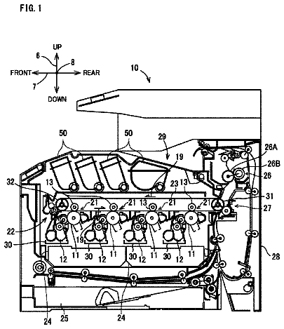
Sheet 1 of 30 from the published document. All sheets in the USPTO PDF
An image forming apparatus forms an image by exposing an image bearer on the basis of image data including at least one predetermined pattern. The image forming apparatus includes a processing device that sets an exposure amount of a plurality of exposure pixels. The predetermined pattern is constituted by the plurality of exposure pixels, and a peripheral region of the predetermined pattern in the image data is constituted by a plurality of non-exposure pixels. The processing device sets an exposure amount of an exposure pixel in a specific region that is adjacent to a boundary between the predetermined pattern and the peripheral region and is constituted by at least one exposure pixel in the predetermined pattern, and an exposure amount of an exposure pixel in a region other than the specific region in the predetermined pattern to values different from each other.
In the related art, an image forming apparatus, in which an image is formed by exposing an image bearer on the basis of image data, is known (for example, refer to Japanese Laid-open Patent Publication No. 2013-257510). However, in the image forming apparatus disclosed in Japanese Laid-open Patent Publication No. 2013-257510, there is room for improvement in reproducibility of an image. Therefore, it is desirable to provide an image forming apparatus and an image forming method capable of improving the reproducibility of an image.
1 of 30 drawing sheets so far from the published document, cropped to the drawing. Every sheet is in the USPTO PDF.
What the patent claimed, word for word. All of it is now free to use.
The present application claims priority to and incorporates by reference the entire contents of Japanese Patent Application No. 2014-116324 filed in Japan on Jun. 5, 2014.
The present invention relates to an image forming apparatus and an image forming method.
In the related art, an image forming apparatus, in which an image is formed by exposing an image bearer on the basis of image data, is known (for example, refer to Japanese Laid-open Patent Publication No. 2013-257510).
However, in the image forming apparatus disclosed in Japanese Laid-open Patent Publication No. 2013-257510, there is room for improvement in reproducibility of an image.
Therefore, it is desirable to provide an image forming apparatus and an image forming method capable of improving the reproducibility of an image.
It is an object of the present invention to at least partially solve the problems in the conventional technology.
According to an aspect of the present invention, there is provided an image forming apparatus that forms an image by exposing an image bearer on the basis of image data including at least one predetermined pattern, including: a processing device that sets an exposure amount of a plurality of exposure pixels, wherein the predetermined pattern is constituted by the plurality of exposure pixels, and a peripheral region of the predetermined pattern in the image data is constituted by a plurality of non-exposure pixels, and the processing device sets an exposure amount of an exposure pixel in a specific region that is adjacent to a boundary between the predetermined pattern and the peripheral region and is constituted by at least one exposure pixel in the predetermined pattern, and an exposure amount of an exposure pixel in a region other than the specific region in the predetermined pattern to values different from each other.
According to another aspect of the present invention, there is provided an image forming apparatus that forms an image by exposing an image bearer on the basis of image data including at least one predetermined pattern, including: a processing device that sets an exposure amount of a plurality of exposure pixels, wherein a peripheral region of the predetermined pattern in the image data is constituted by the plurality of exposure pixels, and the predetermined pattern is constituted by a plurality of non-exposure pixels, and the processing device sets an exposure amount of an exposure pixel in a specific region that is adjacent to a boundary between the predetermined pattern and the peripheral region and is constituted by at least one exposure pixel in the peripheral region, and an exposure amount of an exposure pixel in a region other than the specific region in the peripheral region to values different from each other.
According to still another aspect of the present invention, there is provided an image forming method that forms an image by exposing an image bearer on the basis of image data including at least one predetermined pattern, including: detecting a specific region, which is adjacent to a boundary of the predetermined pattern and a peripheral region of the predetermined pattern in the image data, and includes at least one exposure pixel in the predetermined pattern, the predetermined pattern being constituted by a plurality of exposure pixels, and the peripheral region being constituted by a plurality of non-exposure pixel; and setting an exposure amount of an exposure pixel in the specific region and an exposure amount of an exposure pixel in a region other than the specific region in the predetermined pattern to values different from each other.
The above and other objects, features, advantages and technical and industrial significance of this invention will be better understood by reading the following detailed description of presently preferred embodiments of the invention, when considered in connection with the accompanying drawings.
FIG. 1 is a view illustrating a schematic configuration of a laser printer according to one embodiment;
FIGS. 2A and 2B are views illustrating corotron charging and scorotron charging;
FIGS. 3A to 3C are views (first to third views) illustrating an optical scanning device in FIG. 1 ;
FIG. 4 is a block diagram illustrating a printer control device and a scanning control device;
FIGS. 5A and 5B are views (first and second views) illustrating an image processing unit;
FIG. 6 is a view illustrating an electrostatic latent image measuring device;
FIG. 7 is a cross-sectional view illustrating a vacuum chamber;
FIG. 8A is a graph illustrating a relationship between an acceleration voltage and charging, and FIG. 8B is a graph illustrating a relationship between an acceleration voltage and a charging potential;
FIGS. 9A and 9B are principle models for detection of a charge distribution and a potential distribution by secondary electrons, respectively;
FIGS. 10A to 10D are views (first to fourth views) illustrating a latent image pattern that is formed by the optical scanning device;
FIG. 11 is a view illustrating a measurement example through grid mesh arrangement;
FIGS. 12A and 12B are views (first and second views) illustrating a relationship between a potential and an acceleration voltage;
FIG. 13 is a view illustrating an example of a latent image depth measurement result;
FIGS. 14A and 14B are views (first and second views) illustrating an isolated pattern;
FIGS. 15A to 15C are views (first to third views) illustrating an integrated light amount;
FIGS. 16A and 16B are views illustrating an exposure amount of each exposure pixel in an isolated pattern of Comparative Example 1 and Example 1, and an electrostatic latent image on a photoconductor drum which corresponds to the isolated pattern;
FIGS. 17A and 17B are views illustrating an exposure amount of each exposure pixel in an isolated pattern of Comparative Example 2 and Example 2, and an electrostatic latent image on a photoconductor drum which corresponds to the isolated pattern;
FIG. 18 is a view illustrating an integrated light amount of Comparative Example 3;
FIG. 19 is a view illustrating an integrated light amount (a first integrated light amount) of Example 3;
FIG. 20 is a view illustrating an integrated light amount (a second integrated light amount) of Example 4;
FIG. 21 is a view illustrating an integrated light amount of Comparative Example 4;
FIG. 22 is a view illustrating an integrated light amount (a third integrated light amount) of Example 5;
FIG. 23 is a view illustrating an integrated light amount (a fourth integrated light amount) of Example 6;
FIG. 24 is a view illustrating a specific example of the isolated pattern;
FIG. 25 is a view illustrating an example in which two isolated patterns are adjacent to each other;
FIG. 26A is a view illustrating an exposure method of the related art, and FIGS. 26B to 26D are views (first to third views) illustrating TC exposure, respectively;
FIGS. 27A, 27B, and 27C are views illustrating an exposure amount set value with respect to each exposure pixel and an electrostatic latent image corresponding to the exposure amount set value in Comparative Example 5, Example 7, and Example 8;
FIGS. 28A and 28B are views illustrating an exposure amount set value with respect to each exposure pixel, and an electrostatic latent image corresponding to the exposure amount set value in Comparative Example 6 and Example 9;
FIGS. 29A, 29B, and 29C are views illustrating an exposure amount set value with respect to each exposure pixel, and an electrostatic latent image corresponding to the exposure amount set value in Comparative Example 7, Example 10, and Example 11;
FIGS. 30A and 30B are views illustrating an exposure amount set value with respect to each exposure pixel, and an electrostatic latent image corresponding to the exposure amount set value in Comparative Example 8 and Example 12; and
FIG. 31 is a view illustrating a plurality of isolated patterns for formation of a 45° inclined line.
Hereinafter, one embodiment of the invention will be described on the basis of FIG. 1 to FIG. 31 . FIG. 1 illustrates a schematic configuration of a laser printer 1000 according to the one embodiment.
The laser printer 1000 includes an optical scanning device 1010 as an exposure device, a photoconductor drum 1030 as an image bearer, an electrification charger 1031 , a developing roller 1032 , a transfer charger 1033 , a destaticizing unit 1034 , a cleaning unit 1035 , a toner cartridge 1036 , a paper feeding roller 1037 , a paper feeding tray 1038 , a registration roller pair 1039 , a fixing roller 1041 , a paper ejection roller 1042 , a paper ejection tray 1043 , a scanner 10 (refer to FIG. 4 ) as an original document reading device, a communication control device 1050 , a printer control device 1060 (processing device), and the like. In addition, these components are accommodated at a predetermined position at the inside of a printer casing 1044 .
The communication control device 1050 controls bi-directional communication with a high-level device (for example, a PC) through a network and the like.
The photoconductor drum 1030 is a cylindrical member, and a photosensitive layer is formed on a surface thereof. That is, the surface of the photoconductor drum 1030 is a surface to be scanned. In addition, the photoconductor drum 1030 is configured to rotate in the arrow direction of FIG. 1 .
The electrification charger 1031 , the developing roller 1032 , the transfer charger 1033 , the destaticizing unit 1034 , and the cleaning unit 1035 are disposed in the vicinity of the surface of the photoconductor drum 1030 , respectively. In addition, these components are disposed in the order of the electrification charger 1031 .fwdarw.the developing roller 1032 .fwdarw.the transfer charger 1033 .fwdarw.the destaticizing unit 1034 .fwdarw.the cleaning unit 1035 along a rotation direction of the photoconductor drum 1030 .
The electrification charger 1031 uniformly charges the surface of the photoconductor drum 1030 .
The electrification charger 1031 can create a desired potential through corotron charging as illustrated in FIG. 2A , scorotron charging as illustrated in FIG. 2B , or charging with a roller.
The optical scanning device 1010 scans the surface of the photoconductor drum 1030 , which is charged with the electrification charger 1031 , with laser light that is modulated on the basis of image data (image information) transmitted from a high-level device such as PC. As a result, an electrostatic latent image, which corresponds to the image data, is formed on the surface of the photoconductor drum 1030 . The electrostatic latent image that is formed is moved in a direction of the developing roller 1032 in association with rotation of the photoconductor drum 1030 . In addition, a configuration of the optical scanning device 1010 will be described later.
A toner is stored in the toner cartridge 1036 , and the toner is supplied to the developing roller 1032 .
The developing roller 1032 attaches a toner, which is supplied from the toner cartridge 1036 , to the electrostatic latent image that is formed on the surface of the photoconductor drum 1030 to develop the electrostatic latent image. The electrostatic latent image (hereinafter, referred to as a “toner image” for convenience) to which the toner is attached is moved in a direction of the transfer charger 1033 in association with rotation of the photoconductor drum 1030 .
Recording paper 1040 is stored in the paper feeding tray 1038 . The paper feeding roller 1037 is disposed in the vicinity of the paper feeding tray 1038 , and the paper feeding roller 1037 takes out the recording paper 1040 sheet by sheet from the paper feeding tray 1038 , and transports the recording paper to the registration roller pair 1039 . The registration roller pair 1039 temporarily holds the recording paper 1040 that is taken out by the paper feeding roller 1037 , and transports the recording paper 1040 toward a gap between the photoconductor drum 1030 and the transfer charger 1033 in accordance with rotation of the photoconductor drum 1030 .
A voltage with polarity reversed from that of the toner is applied to the transfer charger 1033 so as to electrically attract the toner on the surface of the photoconductor drum 1030 to the recording paper 1040 . A toner image on the surface of the photoconductor drum 1030 is transferred to the recording paper 1040 by the voltage. The recording paper 1040 to which the toner image is transferred is transported to the fixing roller 1041 .
In the fixing roller 1041 , heat and pressure are applied to the recording paper 1040 , and according to this, the toner is fixed onto the recording paper 1040 . The recording paper 1040 onto which the toner is fixed is transported to the paper ejection tray 1043 through the paper ejection roller 1042 , and is sequentially stacked on the paper ejection tray 1043 .
The destaticizing unit 1034 destaticizes the surface of the photoconductor drum 1030 .
The cleaning unit 1035 removes the toner (residual toner) that is left on the surface of the photoconductor drum 1030 . The surface of the photoconductor drum 1030 from which the residual toner is removed is returned again to a position that faces the electrification charger 1031 .
Next, a configuration of the optical scanning device 1010 will be described. As illustrated in FIG. 3A , as an example, the optical scanning device 1010 includes a light source including a plurality of light-emitting units, a collimator lens, a cylinder lens, a folding mirror, a polygon mirror, a scanning lens L 1 , a scanning lens L 2 , a PD (photo detector) as a light-receiving element, a scanning control device 15 (refer to FIG. 4 ), and the like. These components are assembled at a predetermined position in a housing (not illustrated).
A light beam that is emitted from the light source is made into approximately parallel light by the collimator lens, and is incident to the cylinder lens as a linear imaging forming optical system. The cylinder lens has power only in a sub-scanning direction, allows a plurality of incident light beams to converge only in the sub-scanning direction, and forms an image in the vicinity of a reflection surface of the polygon mirror as a linear image that is elongated in a main-scanning direction.
Here, a motor unit and a drive IC (not illustrated) which drive the polygon mirror are provided. When an appropriate clock is applied to the drive IC, the motor unit is rotated at a predetermined velocity.
When the polygon mirror is rotated by the motor unit at a constant velocity in the arrow direction in FIG. 3A , the plurality of light beams which are reflected from a deflective reflection surface of the polygon mirror become deflected beams, and are deflected at a constant angular velocity.
The deflected beams are transmitted through the scanning lenses L 1 and L 2 as a scanning imaging forming optical system while being deflected, and are reflected from the folding mirror that is a long planar mirror. According to this, an optical path of the beams is bent, and the beams are focused to the surface (surface to be scanned) of the photoconductor drum 1030 as a light spot due to operation of the scanning lenses L 1 and L 2 .
In this manner, the optical scanning device 1010 simultaneously scans a plurality of lines on the surface to be scanned through scanning by one deflective reflection surface of the polygon mirror.
As a result, an electrostatic latent image corresponding to the image data is formed on the photoconductor drum 1030 .
In addition, laser light that is deflected by the polygon mirror is incident to the PD after completion of scanning with respect to one line, or before initiation of scanning with respect to one line. When receiving laser light, the PD converts an amount of light received into an electrical signal, and outputs the electrical signal to the following scanning control device 15 that controls a light source.
Printing data for one line which corresponds to each light-emitting portion of the light source is stored in a buffer memory inside the scanning control device 15 . The printing data is read out for one deflective reflection surface of the polygon mirror, a light beam flickers on a scanning line on the photoconductor drum 1030 in correspondence with the printing data, and an electrostatic latent image is formed in accordance with the scanning line.
As an example of the light source, FIG. 3B illustrates a semiconductor laser array in which four light-emitting portions (semiconductor lasers) are one-dimensionally arranged in a direction perpendicular to an optical axis of the collimator lens.
An example of the light source, FIG. 3C illustrates a surface light-emitting laser array in which 12 light-emitting portions (surface light-emitting lasers: VCSEL) are two-dimensionally arranged along a plane perpendicular to the optical axis of the collimator lens. Here, the 12 light-emitting portions are lined up in a matrix shape including three rows in a horizontal direction (main-scanning direction) and four columns in a vertical direction (sub-scanning direction). In this case, four scanning lines in the vertical direction can be simultaneously scanned by scanning a location on one scanning line with the three light-emitting portions which are lined up in the horizontal direction.
Here, a mechanism in which the electrostatic latent image is formed on the photoconductor will be described in brief. The photoconductor (OPC) is constituted by a charge generating layer (CGL) and a charge transportation layer (CTL) on a conductive support. When the photoconductor is exposed in a state in which a surface thereof is charged, light is absorbed thereto due to a charge generating material (CGM) of the CGL, and thus charge carriers of both positive and negative polarities are generated. Due to an electric field, one of the carriers is injected into the CTL and the other is injected into the conductive support. The carrier, which is injected into the CTL, is moved in the CTL up to a surface of the CTL due to an electric field, and disappears after being coupled with a charge on the surface of the photoconductor. UL has a function of blocking charge injection from the conductive support. According to this, a charge distribution, that is, an electrostatic latent image is formed on the surface of the photoconductor.
Here, the printer control device 1060 will be described.
As illustrated in FIG. 4 , the printer control device 1060 includes a control unit (not illustrated) that integrally controls respective constituent units of the laser printer 1000 , an image processing unit 1060 a , an exposure amount setting unit 1060 b , and the like.
As illustrated in FIG. 5A , the image processing unit 1060 a includes an image processing unit (IPU), a controller unit, a memory unit, and the like.
As illustrated in FIG. 5B , the image processing unit includes a concentration converting unit, a filter unit, a color correcting unit, a selector unit, a grayscale correcting unit, a grayscale processing unit, a unit control unit (not illustrated) that integrally controls the respective units.
The concentration converting unit converts RGB image data transmitted from the scanner 10 or a PC into concentration data by using a look-up table, and outputs the concentration data to the filter unit.
The filter unit performs an image correcting process such as a smoothing process and an edge emphasizing process with respect to the concentration data that is input from the concentration converting unit, and outputs the concentration data to the color correcting unit.
The color correcting unit performs a color correcting (masking) process with respect to image-corrected concentration data that is input from the filter unit, and outputs the data to a selector unit.
The selector unit selects any one of C, M, Y, and K with respect to color-corrected concentration data that is input from the color correcting unit under the control of the unit control unit, and outputs the selected one to the grayscale correcting unit.
The grayscale correcting unit sets a γ curve, from which linear characteristic obtained, with respect to the concentration data of C, M, Y, and K which is input from the selector unit.
The grayscale processing unit performs grayscale processing such as teaser processing with respect to concentration data to which the γ-curve is set and which is input from the grayscale correcting unit.
In addition, the image processing unit outputs image data before image processing or image data (concentration data) after the image processing to the controller unit as necessary.
The controller unit performs processing such as rotation, repeat, aggregation, compression, and expansion with respect to the image data transmitted from the image processing unit, and outputs the image data to the image processing unit.
Various pieces of data such as the look-up table are stored in advance in the memory unit.
The image data, which is subjected to the above-described series of processing in the image processing unit 1060 a , tag data that identifies object information, and the like are output to the exposure amount setting unit 1060 b.
The exposure amount setting unit 1060 b sets an exposure amount of each exposure pixel which is transmitted from the image processing unit 1060 a and is the image data after the image processing, and outputs the image data after setting of the exposure amount, the tag data, and the like to the scanning control device 15 . The exposure amount setting unit 1060 b will be described later in detail. In addition, in the image data that is transmitted from the image processing unit 1060 a to the exposure amount setting unit 1060 b , white portion (non-exposure portion) and a black portion (exposure portion) are designated for each pixel.
The optical scanning device 2 including the scanning control device 15 scans the surface of the photoconductor drum 1030 on the basis of the image data after setting of the exposure amount, the tag data, and the like which are transmitted from the exposure amount setting unit 1060 b to form an electrostatic latent image on the surface of the photoconductor drum 1030 .
As will be described below in detail, the scanning control device 15 performs input of the image data, the tag data, and the like which are transmitted from the exposure amount setting unit 1060 b as necessary to generate drive information of the light source, and drives respective light-emitting portions of the light source by using the drive information.
As illustrated in FIG. 4 , the scanning control device 15 includes a reference clock generating circuit 402 , a pixel clock generating circuit 405 , a light source modulation data generating circuit 407 , a light source selecting circuit 414 , a writing timing signal generating circuit 415 , and a light source driving circuit 400 . In addition, arrows indicate a flow of a representative signal or information, and are not intended to indicate all connection relationships of respective blocks.
The reference clock generating circuit 402 generates a high-frequency clock signal that becomes a reference of the entirety of the scanning control device 15 .
The pixel clock generating circuit 405 is mainly constituted by a PLL circuit, and generates a pixel clock signal on the basis of a synchronization signal s 1 and the high-frequency clock signal that is transmitted from the reference clock generating circuit 402 . The pixel clock signal has the same frequency as that of the high-frequency clock signal, and a phase thereof is equal to a phase of the synchronization signal s 1 . Accordingly, when the image data is synchronized with the pixel clock signal, a recording position for each scanning can be arranged. The pixel clock signal that is generated here is supplied to the light source driving circuit 400 as one of the drive information, and is supplied to the light source modulation data generating circuit 407 and is used a clock signal of recording data s 16 as one of the drive information.
The light source modulation data generating circuit 407 converts the image data to a PM+PWM signal on the basis of the image data or the tag data which is transmitted from the exposure amount setting unit 1060 b in order for an optimal latent image to be formed.
The light source selecting circuit 414 is a circuit that is used in a case where the light source includes a plurality of light-emitting portions. When an image surface of scanning light reaches a scanning distal end, the light source selecting circuit 414 selects a light-emitting portion that is used to sense initiation of the subsequent scanning from the plurality of light-emitting portions (for example, 32 light-emitting portions) and outputs a signal designating the selected light-emitting portion. An output signal s 14 of the light source selecting circuit 414 is supplied to the light source driving circuit 400 as one of the drive information. In addition, in the case of using a single light-emitting portion as the light source, the light source selecting circuit 414 may not be provided.
The writing timing signal generating circuit 415 obtains a writing initiation timing on the basis of the synchronization signal s 1 , and outputs an output signal s 15 , which is the timing signal, to the light source driving circuit 400 as one of the drive information.
The light source driving circuit 400 generates a drive current (for example, a pulse current) of each of the light-emitting portions of the light source on the basis of the drive information, and supplies the drive current to the corresponding light-emitting portion.
Next, description will be given of a device (an electrostatic latent image measuring device) that measures the electrostatic latent image formed on the photoconductor drum with reference to FIG. 6 .
As illustrated in FIG. 6 , the electrostatic latent image measuring device includes a charged particle emitting unit that emits charged particle beams, an exposure unit, a photoconductor sample installation unit, a plurality of voltage power supplies which apply an appropriate voltage to the photoconductor sample, a detection unit that detects primary inverted charged particles, secondary electrons, and the like.
The “charged particles” stated here represent particles such as electron beams or ion beams which are affected by an electric field or a magnetic field. Hereinafter, an example of irradiation using the electron beams will be described.
The charged particle emitting unit includes an electron gun that generates electron beams, a suppressor electrode and an extraction electrode which control the electron beams, an acceleration electrode that controls the energy of the electron beams, a condenser lens that focuses the electron beams generated from the electron gun, a movable aperture that controls an irradiation current relating to the electron beams, a beam blanking electrode that controls ON/OFF of the electron beams, a scanning lens that allows scanning with the electron beams which passes through the beam blanking electrode, and an objective lens that condenses again the electron beams which pass through the scanning lens. A drive power supply (not illustrated) is connected to each of the lenses.
In addition, in the case of the ion beams, a liquid metal ion gun and the like are used instead of the electron gun.
The exposure unit may have the same configuration as that of an actual machine (the optical scanning device 1010 ), and may have a configuration for evaluation only in which charging and exposure conditions can be changed in various manners.
Specifically, the exposure unit includes a light source such as an LD (laser diode) with an oscillation wavelength having sensitivity for the photoconductor, a collimator lens, an aperture, a condenser lens, and the like, and can irradiate the surface of the photoconductor sample with a light spot having a desired beam diameter and a desired beam profile. At this time, appropriate exposure time and exposure intensity are controlled by a light source control circuit.
In addition, the exposure unit may be provided with a scanning mechanism using a galvano mirror or a polygon mirror as an optical system so as to form a linear pattern. In addition, a multi-beam light source such as the LD array and the VCSEL array, which are illustrated in FIG. 3B and FIG. 3C , is also possible.
In addition, a type, in which a scanning mechanism is also provided in a sub-scanning direction in addition to the main-scanning direction and which is capable of forming a two-dimensional exposure pattern, is also possible.
It is preferable that the exposure unit be provided at the outside of a vacuum chamber, in which the charged particle emitting unit is accommodated, in order for vibration of a deflector such as a polygon mirror and an electromagnetic field not to have an effect on an orbit of electron beams. When the exposure unit is spaced away from the charged particle emitting unit, it is possible to suppress an effect of disturbance. It is preferable that light from the exposure unit be incident from an optically transparent incidence window that is provided in the vacuum chamber.
FIG. 7 illustrates a cross-sectional view of the electrostatic latent image measuring device including the exposure unit having the above-described scanning mechanism. As illustrated in FIG. 7 , a glass window, through which light from the light source can be incident to the inside of the vacuum chamber from an outer side, is provided at a position of 45° with respect to a vertical axis of the vacuum chamber, and the exposure unit (optical unit) is disposed at the outside of the vacuum chamber. Here, the exposure unit includes a light source, an optical deflector (polygon scanner in FIG. 7 ), a scanning lens, a synchronization sensing unit, and the like.
An optical housing that holds the exposure unit may have a configuration in which the entirety of the exposure unit is covered with a cover to shield external light (harmful light) that is incident to the inside of the vacuum chamber.
The scanning lens has fθ characteristics, and has a configuration in which when the optical deflector is rotated at a constant velocity, light beams are moved at an approximately constant velocity with respect to the image surface. In addition, the scanning lens has a configuration capable of performing scanning while maintaining an approximately constant beam spot diameter.
The exposure unit is disposed to be spaced from the vacuum chamber. Accordingly, vibration, which occurs during driving of the optical deflector such as the polygon scanner, has a less effect due to direct propagation to the vacuum chamber. Furthermore, although not illustrated in FIG. 7 , when a damper is inserted between a structure and a vibration removal stage, a further higher vibration removal effect can be obtained.
As described above, when the exposure unit includes the scanning mechanism, it is possible to form an arbitrary latent image pattern including a line pattern with respect to a generating line direction of the photoconductor sample.
In addition, the exposure unit may be provided with the synchronization sensing unit that senses scanning beams from the optical deflector so as to form a latent image pattern at a predetermined position.
In addition, a shape of the sample may be a planar surface or a curbed surface.
Hereinafter, description will be given of a method of measuring the electrostatic latent image by using the electrostatic latent image measuring device. First, the photoconductor sample is irradiated with electron beams. When an acceleration voltage |Vacc| is set to an acceleration voltage that is higher than an acceleration voltage at which a secondary electron emission ratio becomes 1, an amount of incident electrons is greater than an amount of emitted electrons, and thus electrons are accumulated in a sample and charge-up is caused (refer to FIG. 8A ). As a result, it is possible to charge the sample in a uniform manner on a negative side. The acceleration voltage and a charging potential have a relationship as illustrated in FIG. 8B , and thus when the acceleration voltage and an irradiation time are appropriately set, it is possible to form the same charging potential as that of an actual machine (optical scanning device 1010 ) in an electrophotography. As an irradiation current is large, it is possible to reach a target charging potential in a short time, and thus irradiation is performed with several nano-amperes.
Then, the amount of incident electrons is lowered to 1/100 times to 1/1000 times so as to observe the electrostatic latent image.
Next, exposure is performed with respect to the photoconductor sample by using the exposure unit. The optical system of the exposure unit is adjusted so as to form a desired beam diameter and a desired beam profile. Necessary exposure energy is a factor that is determined by photoconductor characteristics, and the necessary exposure energy is, in general, approximately 2 mJ/m.sup.2 to 10 mJ/m.sup.2. In the photoconductor having low sensitivity, there is a case that ten and several mJ/m.sup.2 is required. The charging potential or the necessary exposure energy may be set in accordance with the photoconductor characteristics or process conditions.
The exposure conditions in accordance with an actual machine (for example, the optical scanning device 1010 ) in the electrophotography, for example, conditions of an exposure energy density of 0.5 mJ/m.sup.2 to 10 mJ/m.sup.2, a beam spot diameter of 30 μm to 100 μm, a duty, an image frequency, a writing density, an image pattern, and the like may be set by using the above-described components. As the image pattern, it is possible to form various patterns such as a one-dot lattice, 2 by 2, two-dot isolation, and a line in addition to one dot isolation.
According to this, it is possible to form an electrostatic latent image on the photoconductor sample.
That is, the photoconductor sample is scanned with electron beams, secondary electrons which are emitted are detected by a secondary electron detecting unit including a scintillator, and the secondary electrons are converted into electrical signals to observe a contrast image.
In this manner, a contrast image with light and shade in which an amount of secondary electrons detected is much in the non-exposure portion, and an amount of secondary electrons detected is less in the exposure portion, is generated. A dark portion can be considered as a latent image portion due to exposure.
When a charge distribution occurs on a sample surface, an electric field distribution according to a surface charge distribution occurs in a space. According to this, the secondary electrons which are generated in accordance with the incident electrons are pushed back due to the electric field, and thus an amount of the secondary electrons which reach a detector decreases. Accordingly, at a charge leakage site, the exposure portion colors black, and the non-exposure portion colors white, and thus it is possible to measure a contrast image in correspondence with the surface charge distribution.
FIG. 9A illustrates a potential distribution in a space between a charged particle trapping device 24 and a sample SP with contour line display. The surface of the sample SP enters a state of being uniformly charged with a negative polarity except for a portion in which a potential is reduced due to optical attenuation, and a potential with a positive polarity is applied to the charged particle trapping device 24 . Accordingly, in “potential contour line groups indicated by a solid line”, as it is close to the charged particle trapping device 24 from the surface of the sample SP, a “potential becomes high”.
Accordingly, secondary electrons el 1 and el 2 , which are generated at a Q 1 point or a Q 2 point in the drawing which is a “portion that is uniformly charged with a negative polarity” in the sample SP, are attracted by a positive potential of the charged particle trapping device 24 , are displaced as illustrated by an arrow G 1 or an arrow G 2 , and are trapped by the charged particle trapping device 24 .
On the other hand, in FIG. 9A , a Q 3 point is a “portion which is subjected to optical irradiation and in which a negative potential is attenuated”, and arrangement of potential contour lines is similar to “arrangement indicated by a broken line” in the vicinity of the Q 3 point, and in a potential distribution at this portion, “as it is close to the Q 3 point, the potential increases”. In other words, in secondary electrons e 13 which are generated in the vicinity of the Q 3 point, as indicated by an arrow G 3 , an electric force of restricting the secondary electrons toward the sample SP side operates. Accordingly, the secondary electrons e 13 are trapped in a “potential hole” indicated by a potential contour line of a broken line, and are not moved toward the charged particle trapping device 24 . FIG. 9B schematically illustrates the “potential hole”.
That is, with regard to a vector of the secondary electrons (the number of secondary electrons) which are detected by the charged particle trapping device 24 , a portion with a large vector corresponds to a “ground portion (a uniformly and negatively charged portion, a portion represented by the point Q 1 or the point Q 2 in FIG. 9A ) of the electrostatic latent image”, and a portion with a small vector corresponds to an image portion (a portion subjected to optical irradiation, a portion represented by the point Q 3 in FIG. 9A ) of the electrostatic latent image”.
Accordingly, when sampling an electrical signal that can be obtained by the secondary electron detecting unit at the signal processing unit for an appropriate sampling time, as described above, a surface potential distribution V(X, Y) can be specified for each “minute region corresponding to the sampling” with a sampling time T set as a parameter. Accordingly, when the surface potential distribution (potential contrast image): V(X, Y) is configured as two-dimensional image data by using the signal processing unit, and the image data is output by using an output device, it is possible to obtain the electrostatic latent image as a visual image (refer to FIGS. 10A to 10D ).
For example, when expressing the vector of the trapped secondary electrons with “intensity of brightness”, a contrast, in which an image portion of the electrostatic latent image is dark and a ground portion is bright, is obtained, and thus it is possible to express (output) an image with light and shade which corresponds to the surface charge distribution. In addition, when the surface potential distribution is known, it is also possible to know a surface charge distribution.
It is possible to perform measurement with further higher accuracy by measuring a profile of the surface charge distribution or the surface potential distribution.
FIG. 11 illustrates another example of the electrostatic latent image measuring device.
A voltage application unit, which is capable of applying a voltage ±Vsub, is connected to the sample installation unit on a lower side of the photoconductor sample. In addition, a grid mesh is disposed on an upper side of the photoconductor sample so as to suppress an effect of a sample charge on incident electron beams.
FIGS. 12A and 12B are views illustrating a relationship between an incident electron and a sample. FIG. 12A illustrates a case where the acceleration voltage is greater than a surface potential, and FIG. 12B illustrates a case where the acceleration voltage is smaller than the surface potential.
The description continues in the full USPTO document.
About 6,600 words. The USPTO PDF has it with every drawing.
Fees are due 3.5, 7.5 and 11.5 years after grant. This patent expired on November 14, 2025, so the fee marked "not paid" was the one that went unpaid.
IMAGE FORMING APPARATUS AND IMAGE FORMING METHOD
Filed Jun 2015 · published Dec 2015Image forming apparatus and image forming method to form an image based on image data including a pattern
Filed Jun 2015 · granted Nov 2017Earlier publications, parents and continuations. None of them can still be enforced, or this patent would not be listed.
Prior art cited by the examiner or applicant. Useful when you check your own idea for novelty.
Everything on this page comes from the documents linked above.