Background of the invention
1. Field of the invention
One embodiment of the present invention relates to a method of measuring a minute current flowing in a semiconductor device.
One embodiment of the present invention is not limited to the above technical field. The technical field of one embodiment of the invention disclosed in this specification and the like relates to an object, a method, or a manufacturing method. One embodiment of the present invention relates to a process, a machine, manufacture, or a composition of matter. Thus, specific examples of the technical field of one embodiment of the present invention disclosed in this specification include a semiconductor device, a display device, a light-emitting device, a power storage device, a memory device, a method for driving any of them, and a method for manufacturing any of them.
Note that a semiconductor device in this specification and the like generally means a device that can function by utilizing semiconductor characteristics. A semiconductor element such as a transistor, a semiconductor circuit, an arithmetic device, and a memory device are embodiments of a semiconductor device. An imaging device, a display device, a liquid crystal display device, a light-emitting device, an electro-optical device, a power generation device (including a thin film solar cell, an organic thin film solar cell, and the like), and an electronic device may each include a semiconductor device.
2. Description of the related art
Attention has been focused on a technique for forming a transistor using a semiconductor thin film formed over a substrate having an insulating surface (also referred to as thin film transistor (TFT)). Such transistors are applied to a wide range of electronic devices such as an integrated circuit (IC) and an image display device (display device). A semiconductor material typified by silicon is widely known as a material for a semiconductor thin film that can be used for a transistor, and an oxide semiconductor has been attracting attention as well.
For example, Patent Document 1 discloses a technique in which a transistor is manufactured using an amorphous oxide containing In, Zn, Ga, Sn, and the like as an oxide semiconductor.
In order to manufacture semiconductor devices that need charge retention, such as liquid crystal display devices, it is very important to know the characteristics of transistors in an off state (hereinafter referred to as off-state current), and the like. This is because the parameters of a thin film transistor such as channel length and channel width are determined in accordance with the characteristics of the transistor in an off state.
Patent Document 2 discloses an evaluation method in which current values lower than or equal to 1×10.sup.−24 A can be measured.
Patent document
[Patent Document 1] Japanese Published Patent Application No. 2006-165529
[Patent Document 2] Japanese Published Patent Application No. 2011-237418 SUMMARY OF THE INVENTION
Parasitic capacitance is generated, for example, between a drain and a gate, between a drain and a source and between a drain and a substrate in measurement of off-state current of a transistor. It is thus required to reduce the influence of the parasitic capacitance as much as possible and obtain more exact value of the off-state current (leakage current).
In view of the above problem, an object of one embodiment of the present invention is to provide a current measurement method that enables a minute current, to provide an examination method of a semiconductor device employing the current measurement method, to provide a semiconductor device employing the current measurement method, to provide a semiconductor device employing the examination method, to provide a characteristics evaluation circuit, or to provide a novel measurement method. Another object of one embodiment of the present invention is to provide a novel semiconductor device or the like. Note that the descriptions of these objects do not disturb the existence of other objects. In one embodiment of the present invention, there is no need to achieve all the objects. Other objects will be apparent from and can be derived from the description of the specification, the drawings, the claims, and the like.
One embodiment of the present invention includes a transistor under test (a device under test, DUT), a first transistor, a second transistor, and a third transistor. A gate terminal of the first transistor is electrically connected to a first input terminal. One of a source terminal and a drain terminal of the first transistor is electrically connected to a second input terminal. A gate terminal of the transistor under test is electrically connected to a third input terminal. One of a source terminal and a drain terminal of the transistor under test is electrically connected to a fourth input terminal. A gate terminal of the second transistor is electrically connected to the other of the source terminal and the drain terminal of the first transistor and the other of the source terminal and the drain terminal of the transistor under test. One of a source terminal and a drain terminal of the second transistor is electrically connected to one of a source terminal and a drain terminal of the third transistor and an output terminal. A gate terminal of the third transistor is electrically connected to a fifth input terminal. The other of the source terminal and the drain terminal of the third transistor is electrically connected to a sixth input terminal. The other of the source terminal and the drain terminal of the second transistor is electrically connected to a seventh input terminal.
One embodiment of the present invention is a current measurement method in which a first potential is applied to a first terminal of a transistor under test, a second potential is applied to a first terminal of a first transistor, the first transistor is turned on to accumulate a predetermined charge in a node electrically connecting a second terminal of the transistor under test with a second terminal of the first transistor, a third potential of an output terminal of a read circuit electrically connected to the node is measured, the first transistor is turned off, a fourth potential of the output terminal of the read circuit electrically connected to the node is measured, the amount of the charge held by the node is estimated from the amount of change in the potential of the output terminal of the read circuit (e.g., a difference between the third potential and the fourth potential), and a value of current flowing between the first terminal of the transistor under test and the second terminal of the first transistor is calculated from the amount of the charge held by the node.
In the above-described current measurement method, the capacitance between a drain and a substrate of the transistor under test is preferably less than 13.4% of the total capacitance of the node.
In the current measurement method, a channel width of the transistor under test is larger than a channel width of the first transistor.
In the current measurement method, the read circuit includes a second transistor and a third transistor. A first terminal of the second transistor is electrically connected to the node. A first terminal of the third transistor is electrically connected to a second terminal of the second transistor and the output terminal.
In the current measurement method, there preferably is a period in which a potential of a third terminal of the second transistor, a potential of a second terminal of the third transistor, and a potential of a third terminal of the third transistor are equal to one another.
The current measurement method is preferably performed under a constant-temperature environment.
In one embodiment of the present invention, a value of current is calculated from potential change in a predetermined period. The value of a minute current can be measured.
By examining whether or not an electrical element has predefined characteristics using the above current measurement method, defects in a fabricated semiconductor device can be accurately discovered.
A semiconductor device having preferred characteristics can be provided by determining the parameters of an electrical element which is a component of the semiconductor device on the basis of the data on current values obtained by the above current measurement method. According to one embodiment of the present invention, a novel measurement method or a novel semiconductor device can be provided.
Thus, according to one embodiment of the disclosed invention, a variety of technical effects can be obtained.
Note that the description of these effects does not disturb the existence of other effects. One embodiment of the present invention does not necessarily achieve all the effects listed above. Other effects will be apparent from and can be derived from the description of the specification, the drawings, the claims, and the like.
Brief description of the drawings
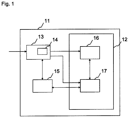
FIG. 1 is a circuit diagram showing an example of a measurement system.
FIG. 2 is a circuit diagram showing an example of a read circuit.
FIG. 3 is a diagram showing input and output characteristics of a source follower circuit.
FIG. 4 is a diagram showing an example of relationship between a potential V.sub.IN and a potential V.sub.OUT, which are potentials of an input terminal IN and an output terminal V.sub.OUT, respectively.
FIG. 5 is a timing chart showing potentials relating to operation of a measurement system.
FIG. 6 is a diagram showing a measurement system and the measurement environment in which temperature change is suppressed.
FIGS. 7A to 7C are diagrams illustrating an example of a structure of a transistor.
FIGS. 8A to 8C are diagrams illustrating an example of a structure of a transistor.
FIGS. 9A to 9C are diagrams illustrating an example of a structure of a transistor.
FIGS. 10A to 10C are diagrams illustrating an example of a structure of a transistor.
FIG. 11 is a view illustrating a movement path of oxygen in an In—Ga—Zn oxide.
FIGS. 12A to 12C are Cs-corrected high-resolution TEM images of a cross section of a CAAC-OS, and FIG. 12D is a cross-sectional schematic view of the CAAC-OS.
FIGS. 13A to 13D are Cs-corrected high-resolution TEM images of a plane of a CAAC-OS.
FIGS. 14A to 14C show structural analysis of a CAAC-OS and a single crystal oxide semiconductor by XRD.
FIGS. 15A and 15B show electron diffraction patterns of a CAAC-OS.
FIG. 16 shows a change in a crystal part of an In—Ga—Zn oxide induced by electron irradiation.
FIGS. 17A to 17F each illustrate an electronic device.
FIGS. 18A and 18B show a structure of a line electrically connecting terminals.
FIGS. 19A and 19B show a conventional structure of a line.
FIG. 20 shows relationship between off-state current and measurement time.
FIG. 21 shows relationship between off-state current and measurement time.
FIG. 22 shows relationship between off-state current and temperature.
FIG. 23 shows relationship between output potential of a source follower and measurement time.
FIG. 24 shows relationship between off-state current and temperature.
FIG. 25 shows relationship between off-state current and temperature.
Detailed description of the invention
Hereinafter, embodiments will be described with reference to drawings. However, the embodiments can be implemented with various modes. It will be readily appreciated by those skilled in the art that modes and details can be changed in various ways without departing from the spirit and scope of the present invention. Thus, the present invention should not be interpreted as being limited to the following description of the embodiments.
In the drawings, the size, the layer thickness, or the region is exaggerated for clarity in some cases. Therefore, embodiments of the present invention are not limited to such a scale. Note that drawings are schematic views of ideal examples, and the embodiments of the present invention are not limited to the shape or the value illustrated in the drawings.
Note that in this specification, ordinal numbers such as “first”, “second”, and “third” are used in order to avoid confusion among components, and the terms do not limit the components numerically.
Note that in this specification, terms for describing arrangement, such as “over” “above”, “under”, and “below”, are used for convenience in describing a positional relation between components with reference to drawings. The positional relation between components is changed as appropriate in accordance with a direction in which each component is described. Thus, there is no limitation on terms used in this specification, and description can be made appropriately depending on the situation.
In this specification and the like, a transistor is an element having at least three terminals of a gate, a drain, and a source. The transistor has a channel region between a drain (a drain terminal, a drain region, or a drain electrode) and a source (a source terminal, a source region, or a source electrode), and current can flow through the drain region, the channel region, and the source region. Note that in this specification and the like, a channel region refers to a region through which current mainly flows.
Functions of a source and a drain might be switched when transistors having different polarities are employed or a direction of current flow is changed in circuit operation, for example. Therefore, the terms “source” and “drain” can be replaced with each other in this specification.
In this specification, the channel length refers to, for example, a distance between a source (a source region or a source electrode) and a drain (a drain region or a drain electrode) in a region where a semiconductor (or a portion where a current flows in a semiconductor when a transistor is on) and a gate electrode overlap with each other or a region where a channel is formed in a top view of the transistor. Note that in one transistor, channel lengths in all regions are not necessarily the same. In other words, the channel length of one transistor is not limited to one value in some cases. Therefore, in this specification, the channel length is any one of values, the maximum value, the minimum value, or the average value in a region where a channel is formed.
In this specification, the channel width refers to, for example, the width of a source or a drain in a region where a semiconductor (or a portion where a current flows in a semiconductor when a transistor is on) and a gate electrode overlap with each other or a region where a channel is formed. Note that in one transistor, channel widths in all regions do not necessarily have the same value. In other words, a channel width of one transistor is not fixed to one value in some cases. Therefore, in this specification, a channel width is any one of values, the maximum value, the minimum value, or the average value in a region where a channel is formed.
Note that depending on transistor structures, a channel width in a region where a channel is formed actually (hereinafter referred to as an effective channel width) is different from a channel width shown in a top view of a transistor (hereinafter referred to as an apparent channel width) in some cases. For example, in a transistor having a three-dimensional structure, an effective channel width is greater than an apparent channel width shown in a top view of the transistor, and its influence cannot be ignored in some cases. For example, in a miniaturized transistor having a three-dimensional structure, the proportion of a channel region formed in a side surface of a semiconductor is higher than the proportion of a channel region formed in a top surface of a semiconductor in some cases. In that case, an effective channel width obtained when a channel is actually formed is greater than an apparent channel width shown in the top view.
In a transistor having a three-dimensional structure, an effective channel width is difficult to measure in some cases. For example, to estimate an effective channel width from a design value, it is necessary to assume that the shape of a semiconductor is known as an assumption condition. Therefore, in the case where the shape of a semiconductor is not known accurately, it is difficult to measure an effective channel width accurately.
Therefore, in this specification, in a top view of a transistor, an apparent channel width that is a width of a portion where a source and a drain face each other in a region where a semiconductor and a gate electrode overlap with each other is referred to as a surrounded channel width (SCW) in some cases. In this specification, in the case where the term “channel width” is simply used, it may denote a surrounded channel width and an apparent channel width. In the case where the term “channel width” is simply used, it may denote an effective channel width in some cases. Note that the values of a channel length, a channel width, an effective channel width, an apparent channel width, a surrounded channel width, and the like can be determined by obtaining and analyzing a cross-sectional TEM image and the like.
Note that in the case where electric field mobility, a current value per channel width, and the like of a transistor are obtained by calculation, a surrounded channel width may be used for the calculation. In that case, a value different from one in the case where an effective channel width is used for the calculation is obtained in some cases. Embodiment 1
In this embodiment, an example of a current measurement method according to one embodiment of the present invention and a measurement system used for the current measurement method will be described with reference to FIG. 1 .
<Measurement System>
First, an example of a measurement system used for the current measurement method according to one embodiment of the present invention will be described with reference to FIG. 1 . The configuration of the measurement system can be used as that of a circuit for characteristic evaluation. Note that the measurement system described below is just an example.
A measurement system illustrated in FIG. 1 includes a transistor 100 , a transistor 101 , a transistor 102 , and a transistor 103 . A gate terminal of the transistor 100 is electrically connected to an input terminal IN_ 1 . One of a source terminal and a drain terminal of the transistor 100 is electrically connected to an input terminal IN_ 2 . A gate terminal of the transistor 101 is electrically connected to an input terminal IN_ 3 . One of a source terminal and a drain terminal of the transistor 101 is electrically connected to an input terminal IN_ 4 . A gate terminal of the transistor 102 is electrically connected to the other of the source terminal and the drain terminal of the transistor 100 and the other of the source terminal and the drain terminal of the transistor 101 . One of a source terminal and a drain terminal of the transistor 102 is electrically connected to one of a source terminal and a drain terminal of the transistor 103 and an output terminal OUT. A gate terminal of the transistor 103 is electrically connected to an input terminal IN_ 5 . The other of the source terminal and the drain terminal of the transistor 103 is electrically connected to an input terminal IN_ 6 . The other of the source terminal and the drain terminal of the transistor 102 is electrically connected to an input terminal IN_ 7 . A node connected to the gate terminal of the transistor 102 (i.e., a node connected to the gate terminal of the transistor 102 , the other of the source terminal and the drain terminal of the transistor 100 , and the other of the source terminal and the drain terminal of the transistor 101 ) is referred to as a node FN. Note that the transistor 101 is a transistor under test.
In order to measure a minute current, the current needs to be increased to the extent that electric charge transferred by such a small amount of current. In order to increase current per unit channel width to be measured, the channel width of the transistor 101 under test is extremely increased. A change in the amount of charge in the node FN is measured for a long time to estimate an off-state current with the use of the transistor whose channel width is extremely large (1 m in this embodiment).
A circuit for writing potentials to the node FN (also referred to as a write circuit) includes the transistor 100 . A circuit for reading the potential of the node FN (also referred to as a read circuit) includes the transistors 102 and 103 .
The transistor 100 included in the write circuit is formed at the same time as the transistor 101 under test. Since the channel width of the transistor 100 is smaller than that of the transistor 101 , contribution of the channel width to leakage current can be ignored.
The read circuit preferably has a small input capacitance and measures the potential of the node FN with high accuracy. A source follower circuit including the transistors 102 and 103 is used as the read circuit in this embodiment. The transistors 102 and 103 are formed at the same time as the transistor 101 under test.
Because parasitic capacitance is generated in the lines electrically connecting the terminals, the width of the line (terminal) is decreased to reduce the parasitic capacitance. The width of the line (terminal) is preferably 20 nm to 0.5 μm, inclusive. When the width of the line (terminal) is reduced, the capacitance between a drain and a substrate can also be reduced. The drain-substrate capacitance is preferably less than 13.4% of the total capacitance of the node FN, more preferably less than 13.0%. The width of the line (terminal) is set to 0.35 μm in this embodiment. The capacitance of the node FN is set to 5×10.sup.−10 F.
<Current Measurement Method>
Next, an example of a current measurement method using the above-described system of measurement will be described with reference to FIG. 1 and FIG. 2 . Note that the current measurement method below is only an example.
First, potential difference is generated between the input terminals IN_ 1 and IN_ 2 to turn on the transistor 100 , thereby writing the potential of the input terminal IN_ 2 to the node FN. At that time, the input terminals IN_ 3 and IN_ 4 are controlled so that the transistor 101 is off. The input terminals IN_ 1 and IN_ 2 are then controlled to turn off the transistor 100 , so that the potential of the node FN, i.e., a potential V.sub.FN, is held. The potentials of the input terminals IN_ 3 and IN_ 4 are fixed during a measurement period that follows. In contrast, the potential V.sub.FN is not fixed (i.e., the node FN is in a floating state) during the measurement period. As a result, charge flows by the off-state current of the transistor 101 , and the potential V.sub.FN changes over time. That is, the potential V.sub.FN changes in accordance with the change in the amount of charge held in the node FN. The potential of the output terminal OUT, i.e., a potential V.sub.OUT changes accordingly.
Next, the amount of change in the potential V.sub.FN is obtained from the change in the potential V.sub.OUT; accordingly, the potential V.sub.FN is obtained from the potential V.sub.OUT. In order to obtain the potential V.sub.FN from the potential V.sub.OUT, the input and output characteristics of an independent read circuit as in FIG. 2 , which is a source follower circuit, is independently evaluated in advance.
In this embodiment, the input and output characteristics of the read circuit illustrated in FIG. 2 is independently evaluated by varying the potential of an input terminal IN (i.e., a potential V.sub.IN) and the potential of an input terminal V.sub.REF (i.e., a potential V.sub.REF). Note that the potentials of an input terminal VDD and an input terminal VSS are 3 V and −2 V, respectively. The potential V.sub.IN is varied by 0.1 V from −3 V to 4 V. The potential V.sub.REF is varied by 0.5 V from −2.5 V to 0 V. Note that the potential V.sub.IN corresponds to the potential V.sub.FN of the node FN in FIG. 1 .
FIG. 3 shows an example of the input and output characteristics of the source follower circuit.
A linear approximation formula of the potentials V.sub.IN and V.sub.OUT (see FIG. 4 ) is calculated from the input and output characteristics of the source follower circuit in FIG. 3 . Leakage current is estimated with reference to data at the time when the potential V.sub.REF is set to −1.0 V.
A value of the potential V.sub.OUT is assigned to x of the liner appropriation formula in FIG. 4 , thereby obtaining y which is the potential V.sub.IN. The initial and last values of the potential V.sub.OUT in the measurement period are assigned thereto, thereby obtaining change in the potential V.sub.IN.
Leakage current of the transistor 101 is estimated by the formula below.
I = C Δ V FN Δ t [ Formula 1 ]
In the formula, I represents leakage current of the transistor 101 . C represents the capacitance of the node FN. ΔV.sub.FN represents the amount of change in the potential of the node FN. At represents the length of the measurement period.
Note that in order to measure the capacitance of the node FN, a configuration of a part around the node FN is fabricated in advance, and the capacitance of the configuration is measured using a semiconductor device analyzer (B1500A manufactured by Agilent Technologies, Inc.).
The leakage current of the transistor 101 is obtained from the capacitance of the node FN, the amount of change in the potential of the node FN, and the measurement period.
FIG. 5 shows relationships between potentials of the terminals in the write period and the subsequent measurement period.
First, the measurement system is turned on, a period D passes, and then the potential of the input terminal IN_ 2 is changed from low to high. In this embodiment, the low potential and the high potential of the input terminal IN_ 2 are set to 1 V and 2 V, respectively, and the length of the period D is set to 3 seconds.
After the measurement system is turned on and a period A (>the period D) passes, the potential of the input terminal IN_ 1 is changed from low to high. In this embodiment, the low potential and the high potential of the input terminal IN_ 1 are set to −3 V and 5 V, respectively, and the length of the period A is set to 8 seconds. When the potential of the input terminal IN_ 1 becomes high, the transistor 100 is turned on and the potential of the input terminal IN_ 2 is written to the node FN (i.e., charge is accumulated in the node FN).
At the same time, the potentials of the input terminals IN_ 5 and IN_ 6 are changed from high to low, and the potential of the input terminal IN_ 7 is changed from low to high. In this embodiment, the low potential and the high potential of the input terminal IN_ 5 are set to −1.5 V and 1.5 V, respectively; the low potential and the high potential of the input terminal IN_ 6 are set to −2 V and 1.5 V, respectively; and the low potential and the high potential of the input terminal IN_ 7 are set to 1.5 V and 3 V, respectively. Here, the read circuit including the transistors 102 and 103 fills the linear appropriation formula in FIG. 4 , and the potential of the node FN can be estimated from the potential V.sub.OUT.
The reason why the levels of signals of the input terminals IN_ 5 , IN_ 6 , and IN_ 7 are changed at the time when the input terminal IN_ 1 is changed from high to low is to monitor the potential \T.sub.our at the time when the potential of the node FN is 2 V (i.e., the potential at the time of writing).
After the potential of the input terminal IN_ 1 becomes high and a period B passes, the potential of the input terminal IN_ 1 becomes low and the transistor 100 is turned off. Note that the potential V.sub.FN is not fixed (i.e., the node FN is in a floating state) because the potentials of the input terminals IN_ 3 and IN_ 4 are fixed. In this embodiment, the potentials of the input terminals IN_ 3 and IN_ 4 are set to −3 V and 0 V, respectively, and the length of the period B is set to 10 seconds.
After the potential of the input terminal IN_ 2 becomes high and a period E passes, the potential of the input terminal IN_ 2 is changed to low. The period E is set to 20 seconds in this embodiment.
After the potentials of the input terminals IN_ 5 and IN_ 6 become low, the potential of the input terminal IN_ 7 becomes high, and the period F passes, the potentials of the input terminals IN_ 5 and IN_ 6 become high and the potential of the input terminal IN_ 7 becomes low. The period F is set to 15 seconds in this embodiment.
The reason why the potentials of the input terminals IN_ 5 and IN_ 6 are changed to high and the potential of the input terminal IN_ 7 is changed to low is to suppress bias deterioration (the potentials of the input terminals IN_ 5 , IN_ 6 , and IN_ 7 are all 1.5 V).
Although the total length of the periods D and E is equal to that of the periods A and F, they are not necessarily equal and may be different.
In the period during which the potential of the node FN is 2 V, which is a potential at the time of writing, a signal Trigger for reading the potential V.sub.OUT is transmitted to a measurement device, so that the potential V.sub.OUT is read by the measurement device. Note that it takes a few seconds for the measurement device to read the potential V.sub.OUT after the signal Trigger is transmitted to the measurement device. Thus, reading of the potential V.sub.OUT needs to be completed in the period during which the input terminals IN_ 5 and IN_ 6 are low and the input terminal IN_ 7 is high. Furthermore, accurate data might not be obtained even after the signal Trigger is transmitted to the measurement device at the same time when the input terminals IN_ 5 and IN_ 6 become low and the input terminal IN_ 7 becomes high. For this reason, it is preferable to transmit the signal Trigger to the measurement device shortly (e.g., a second) after the input terminals IN_ 5 and IN_ 6 become low and the input terminal IN_ 7 becomes high.
Through the above process, first writing and reading are completed.
Next, after the potential of the input terminal IN_ 2 becomes low and the period F passes, the potential of the input terminal IN_ 2 is changed to high.
After the potential of the input terminal IN_ 1 is changed to low and a period C passes, the potential of the input terminal IN_ 1 is changed to high. The period C is set to 25 seconds in this embodiment. When the potential of the input terminal IN_ 1 becomes high, the transistor 100 is turned on to write the potential of the input terminal IN_ 2 to the node FN.
After the potentials of the input terminals IN_ 5 and IN_ 6 become high, the potential of the input terminal IN_ 7 is low, and a period E passes, the potentials of the input terminals IN_ 5 and IN_ 6 are changed to low and the potential of the input terminal IN_ 7 is changed to high. The read circuit including the transistors 102 and 103 fill the linear appropriation formula in FIG. 4 at that time, and the potential of the node FN can be estimated from the potential V.sub.OUT. Note that in the period during which the input terminals IN_ 5 and IN_ 6 are low and the input terminal IN_ 7 is high, the signal Trigger for reading the potential V.sub.OUT is transmitted to a measurement device, so that the potential V.sub.OUT is read by the measurement device.
After the input terminal IN_ 1 becomes high and the period B passes, the potential of the input terminal IN_ 1 is changed low, so that the transistor 100 is turned off.
After the potential of the input terminal IN_ 2 becomes high and the period E passes, the potential of the input terminal IN_ 2 is changed to low.
After the period F during which the potentials of the input terminals IN_ 5 and IN_ 6 are low and the potential of the input terminal IN_ 7 is high, the potentials of the input terminals IN_ 5 and IN_ 6 are changed to high and the potential of the input terminal IN_ 7 is changed to low.
Through the above process, second writing and reading are completed. The number of times of writing, which is two in this embodiment, is not limited to and may be one or three or more.
After the potentials of the input terminals IN_ 5 and IN_ 6 are changed to high, the potential of the input terminal IN_ 7 is changed to low, and a period G passes, the potentials of the input terminals IN_ 5 and IN_ 6 are changed to low and the potential of the input terminal IN_ 7 is changed to high. The length of the period G is set to 26 seconds in this embodiment.
After the potentials of the input terminals IN_ 5 and IN_ 6 become low, the potential of the input terminal IN_ 7 becomes high, and the period F passes, the potentials of the input terminals IN_ 5 and IN_ 6 is changed to high and the potential of the input terminal IN_ 7 is changed to low.
Although the lengths of periods E and G are different from each other in this embodiment, they may be equal to each other.
Next, the measurement period (data hold period) is described. The measurement period is a period after the signal Trigger is changed from low to high and before the signal Trigger is changed from low to high next. The length of the measurement period is 300 seconds in this embodiment. Note that in the case where the measurement time is an hour, 300-second measurement is performed 12 cycles to read out the potential V.sub.OUT every 300 seconds, so that accurate data is obtained.
Note that the influence of noise (output voltage variable according to the temperature) due to measurement environment can be reduced by a method as shown in FIG. 6 : temperature of a measurement sample including a characteristics evaluation circuit is suppressed so that the sample can be kept at a constant temperature using an inert oven. In addition, peripheral air of the measurement system is also kept constant temperature using a constant-temperature air generator.
Specifically, the measurement sample is set in the inert oven to keep the sample temperature constant. The humidity in the inert oven can be reduced by supplying dry air to the inert oven at that time, which provides a low-humidity measurement environment. The sample is connected to a transit portion with a flat cable. The transit portion is connected to a first measurement instrument and a second measurement instrument with coaxial cables. The first measurement instrument transmits a signal for transmitting data of the sample to the transit portion via the coaxial cable. The data of the sample is supplied to the second measurement instrument via the transit portion. The second measurement instrument reads out the potential V.sub.OUT. Note that the measurement system is preferably kept at a constant temperature. In order to keep the measurement system at a constant temperature, for example, the measurement system is covered by a heat insulator, a plastic corrugated cardboard, or the like, and constant-temperature air is supplied using the constant-temperature air generator and a duct cable. Note that it is preferable that the measurement system not be entirely covered by the heat insulator, the plastic corrugated cardboard, or the like so that a small amount of constant-temperature air can flow off to the outside.
By the above-described method, a minute current flowing in electrical elements can be measured using a current value estimated from measurement and converted to a current value per micrometer of channel width. For example, a current value of 1 zA (zeptoampere, 1 zA is equal to 10.sup.−21 A) or smaller, or even 1 yA (yoctoampere, 1 yA is equal to 10.sup.−24 A) or smaller can be measured by the method described in this embodiment.
The structures, methods, and the like described in this embodiment can be combined as appropriate with any of the other structures, methods, and the like described in this embodiment or any of the structures, methods, and the like described in the other embodiments. Embodiment 2
In this embodiment, a semiconductor device (a transistor) using an oxide semiconductor is described with reference to FIGS. 7A to 7C . Although a top-gate transistor is described as an example, the structure of a transistor is not limited to a top-gate structure.
FIGS. 7A to 7C illustrate a structure example of a transistor 60 that includes a channel formation region in an oxide semiconductor film. FIG. 7A is a top view of the transistor 60 . Note that insulating films are not illustrated in FIG. 7A in order to clarify the layout of the transistor 60 . FIG. 7B is a cross-sectional view along the dashed-dotted line A 1 -A 2 in the top view in FIG. 7A . FIG. 7C is a cross-sectional view along the dashed-dotted line A 3 -A 4 in the top view in FIG. 7A .
As illustrated in FIGS. 7A to 7C , the transistor 60 includes oxide semiconductor films 92 a to 92 c that are stacked in this order over an insulating film 91 formed over a substrate 97 ; a conductive film 93 and a conductive film 94 that are electrically connected to the oxide semiconductor film 92 b and function as a source electrode and a drain electrode; an oxide semiconductor film 92 c over the oxide semiconductor film 92 b , the conductive film 93 , and the conductive film 94 ; an insulating film 95 that functions as a gate insulating film and is located over the oxide semiconductor film 92 c ; and a conductive film 96 that functions as a gate electrode, lies over the insulating film 95 , and overlaps with the oxide semiconductor films 92 a to 92 c . Note that the substrate 97 may be a glass substrate, a semiconductor substrate, or the like or may be an element substrate where semiconductor elements are formed over a glass substrate or on a semiconductor substrate.
FIGS. 8A to 8C illustrate another specific example of the structure of a transistor. FIG. 8A is a top view of a transistor 70 . Note that insulating films are not illustrated in FIG. 8A in order to clarify the layout of the transistor 70 . FIG. 8B is a cross-sectional view along the dashed line A 1 -A 2 in the top view in FIG. 8A . FIG. 8C is a cross-sectional view along the dashed line A 3 -A 4 in the top view in FIG. 8A .
As illustrated in FIGS. 8A to 8C , the transistor 70 includes the oxide semiconductor films 92 a , 92 c , and 92 c that are stacked in this order over the insulating film 91 formed over the substrate 97 ; the conductive film 93 and the conductive film 94 that are electrically connected to the oxide semiconductor film 92 b and function as a source electrode and a drain electrode; the oxide semiconductor film 92 c over the oxide semiconductor film 92 b , the conductive film 93 , and the conductive film 94 ; an insulating film 95 that functions as a gate insulating film and is located over the oxide semiconductor film 92 c and the conductive films 93 and 94 ; and the conductive film 96 that functions as a gate electrode, lies over the insulating film 95 , and overlaps with the oxide semiconductor films 92 a to 92 c.
FIGS. 9A to 9C illustrate another specific example of the structure of a transistor. FIG. 9A is a top view of a transistor 80 . Note that various insulating films are not illustrated in FIG. 9A in order to clarify the layout of the transistor 80 . FIG. 9B is a cross-sectional view along the dashed line A 1 -A 2 in the top view in FIG. 9A . FIG. 9C is a cross-sectional view along the dashed line A 3 -A 4 in the top view in FIG. 9A .
As shown in FIGS. 9A to 9C , a transistor 80 includes insulating films 98 and 99 over the transistor 70 shown in FIGS. 7A to 7C . The insulating film 98 is formed using a material similar to that of the insulating film 95 serving as a gate insulating film. Thus, interface electric charge generated by a bandgap difference between the films can be suppressed.
The description continues in the full USPTO document.
 Lapsed, fee not paid4 drawings